Physics Exam > Physics Notes > Physics for IIT JAM, UGC - NET, CSIR NET > Junction Field Effect Transistor - Semiconductor Devices, CSIR-NET Physical Sciences
Junction Field Effect Transistor - Semiconductor Devices, CSIR-NET Physical Sciences | Physics for IIT JAM, UGC - NET, CSIR NET PDF Download
- In 1945, Shockley had an idea for making a solid state device out of semiconductors.
- He reasoned that a strong electrical field could cause the flow of electricity within a nearby semiconductor.
- He tried to build one, but it didn't work.
- Three years later, Brattain & Bardeen built the first working transistor, the germanium point-contact transistor, which was designed as the junction (sandwich) transistor.
- In 1960 Bell scientist John Atalla developed a new design based on Shockley's original field-effect theories.
- By the late 1960s, manufacturers converted from junction type integrated circuits to field effect devices.
- Field effect devices are those in which current is controlled by the action of an electron field, rather than carrier injection.
- Field-effect transistors are so named because a weak electrical signal coming in through one electrode creates an electrical field through the rest of the transistor.
- The FET was known as a “unipolar” transistor.
- The term refers to the fact that current is transported by carriers of one polarity (majority), whereas in the conventional bipolar transistor carriers of both polarities (majority and minority) are involved.
The family of FET devices may be divided into :
- Junction FET
- Depletion Mode MOSFET
- Enhancement Mode MOSFET
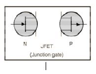
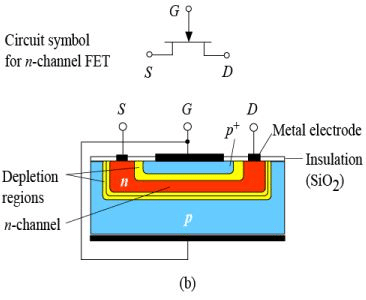
Junction FETs (JFETs)
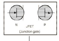
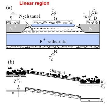
- JFETs consists of a piece of high-resistivity semiconductor material (usually Si) which constitutes a channel for the majority carrier flow.
- Conducting semiconductor channel between two ohmic contacts – source & drain
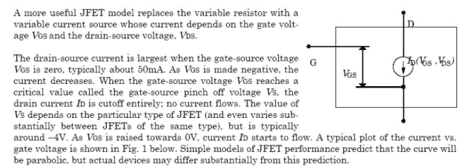
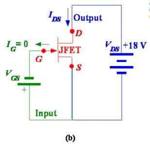
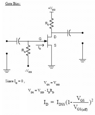
- The magnitude of this current is controlled by a voltage applied to a gate, which is a reverse-biased.
- The fundamental difference between JFET and BJT devices: when the JFET junction is reverse-biased the gate current is practically zero, whereas the base current of the BJT is always some value greater than zero.
Junction FETs
- JFET is a high-input resistance device, while the BJT is comparatively low.
- If the channel is doped with a donor impurity, n-type material is formed and the channel current will consist of electrons.
- If the channel is doped with an acceptor impurity, p-type material will be formed and the channel current will consist of holes.
- N-channel devices have greater conductivity than pchannel types, since electrons have higher mobility than do holes; thus n-channel JFETs are approximately twice as efficient conductors compared to their p-channel counterparts.
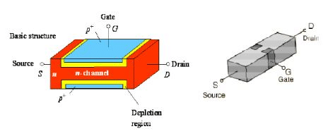
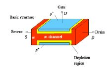
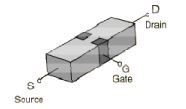
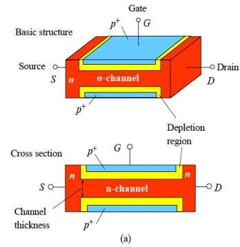
Basic Structure of FETs
- In addition to the channel, a JFET contains two ohmic contacts: the source and the drain.
- The JFET will conduct current equally well in either direction and the source and drain leads are usually interchangeable.
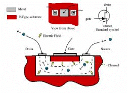
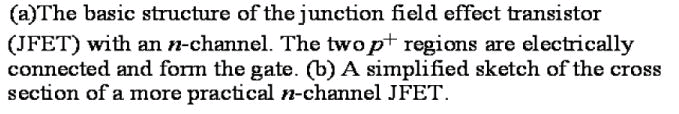
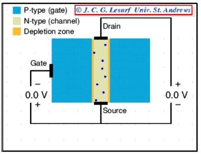
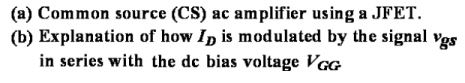
N - Channel JFET
- This transistor is made by forming a channel of N-type material in a P-type substrate.
- Three wires are then connected to the device.
- One at each end of the channel.
- One connected to the substrate.
- In a sense, the device is a bit like a PN-junction diode, except that there are two wires connected to the Ntype side.
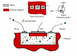
How JFET Function
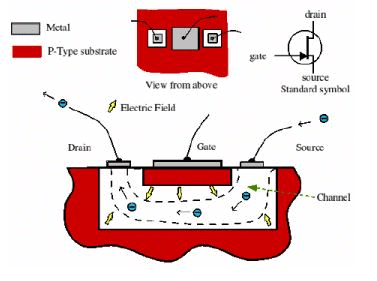
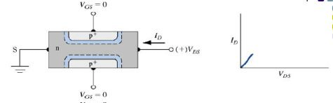
- The gate is connected to the source.
- Since the pn junction is reversebiased, little current will flow in the gate connection.
- The potential gradient established will form a depletion layer, where almost all the electrons present in the n-type channel will be swept away.
- The most depleted portion is in the high field between the G and the D, and the leastdepleted area is between the G and the S.
- Because the flow of current along the channel from the (+ve) drain to the (-ve) source is really a flow of free electrons from S to D in the n-type Si, the magnitude of this current will fall as more Si becomes depleted of free electrons.
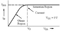
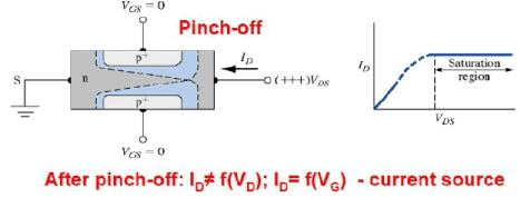
- There is a limit to the drain current (ID) which increased VDS can drive through the channel.
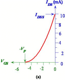
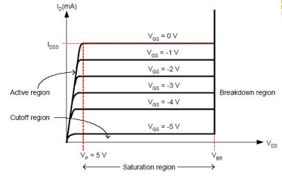
- This limiting current is known as IDSS (Drain-to-Source current with the gate shorted to the source).
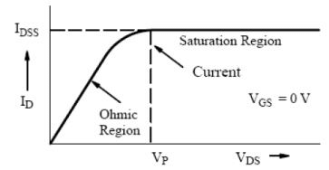
- The output characteristics of an n-channel JFET with the gate short-circuited to the source.
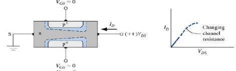
- The initial rise in ID is related to the buildup of the depletion layer as VDS increases.
- The curve approaches the level of the limiting current IDSS when ID begins to be pinched off.
- The physical meaning of this term leads to one definition of pinch-off voltage, VP , which is the value of VDS at which the maximum IDSS flows.
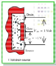
- With a steady gate-source voltage of 1 V there is always 1 V across the wall of the channel at the source end.
- A drain-source voltage of 1 V means that there will be 2 V across the wall at the drain end. (The drain is ‘up’ 1V from the source potential and the gate is 1V ‘down’, hence the total difference is 2V.)
- The higher voltage difference at the drain end means that the electron channel is squeezed down a bit more at this end.
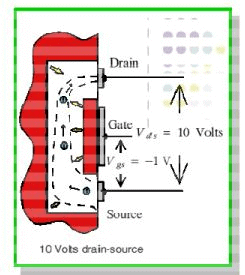
- When the drain-source voltage is increased to 10V the voltage across the channel walls at the drain end increases to 11V, but remains just 1V at the source end.
- The field across the walls near the drain end is now a lot larger than at the source end.
- As a result the channel near the drain is squeezed down quite a lot.
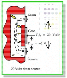
- Increasing the source-drain voltage to 20V squeezes down this end of the channel still more.
- As we increase this voltage we increase the electric field which drives electrons along the open part of the channel.
- However, also squeezes down the channel near the drain end. l This reduction in the open channel width makes it harder for electrons to pass.
- As a result the drain-source current tends to remain constant when we increase the drain-source voltage.
- Increasing VDS increases the widths of depletion layers, which penetrate more into channel and hence result in more channel narrowing toward the drain.
- The resistance of the n-channel, RAB therefore increases with VDS.
- The drain current: IDS = VDS/RAB
- ID versus VDS exhibits a sublinear behavior, see figure for VDS < 5V.
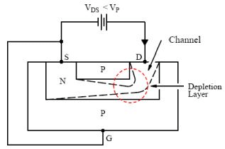
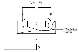
- The pinch-off voltage, VP is the magnitude of reverse bias needed across the p+n junction to make them just touch at the drain end.
- Since actual bias voltage across p+n junction at drain end is VGD, the pinch-off occur whenever: VGD = -VP.
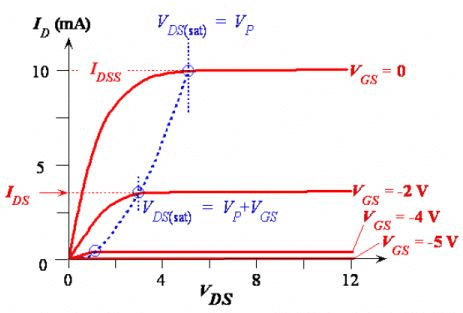
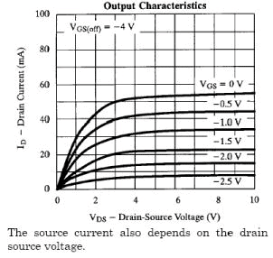
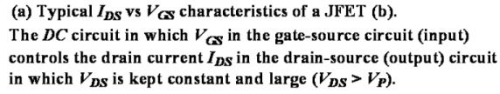
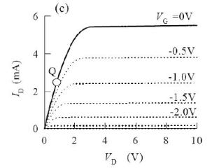
Typical ID vs VDs characteristics of a JFET for various fixed gate voltages VGS.
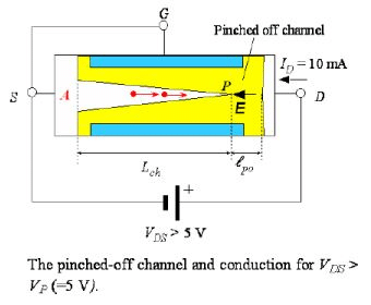
- Beyond VDS = VP, there is a short pinch-off channel of length, ℓpo.
- As VDS increases, most of additional voltage simply drops across ℓpo as this region is depleted of carriers and hence highly resistive.
- Voltage drop across channel length, Lch remain as VP.
- Beyond pinch-off then ID = VP/RAP (VDS>VP).
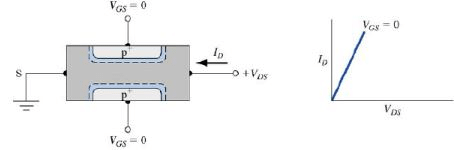
- What happen when negative voltage, says VGS = -2V, is applied to gate with respect to source (with VDS=0).
- The p+n junction are now reverse biased from the start, the channel is narrower, and channel resistance is now larger than in the VGS = 0 case.
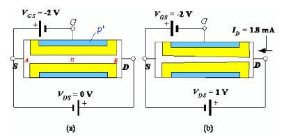
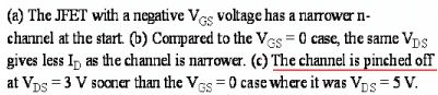
- The drain current that flows when a small VDS applied (Fig b) is now smaller than in VGS= 0 case.
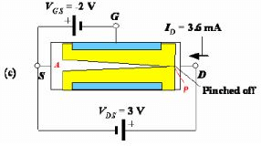
- Applied VDS= 3 V to pinch-off the channel (Fig c).
- When VDS= 3V, VGD across p+n junction at drain end is -5V, which is –VP, so channel becomes pinch-off.
- Beyond pinch-off, ID is nearly saturated just as in the VGS=0 case.
- Pinch-off occurs at VDS= VDS(sat), VDS(sat)= VP+VGS, where VGS is –ve voltage (reducing VP).
- For VDS>VDS(sat), ID becomes nearly saturated at value as IDS.
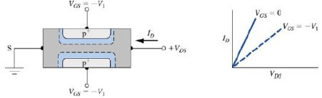
- Beyond pinch-of, with –ve VGS, IDS is
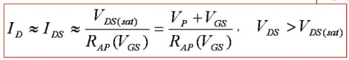
- Where RAP(VGS) is the effective resistance of the conducting n-channel from A to P, which depends on channel thickness and hence VGS.
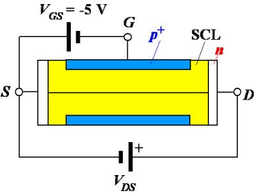
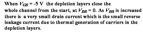
- When VGS= -VP= -5V with VDS= 0, the two depletion layers touch over the entire channel length and the whole channel is closed.
- The channel said to be off.
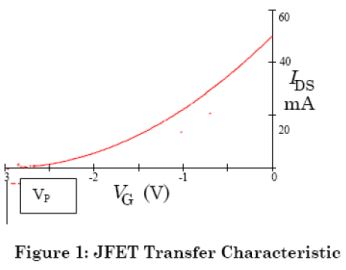
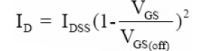
- There is a convenient relationship between IDS and VGS.
- Beyond pinch-off
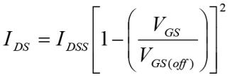
- Where IDSS is drain current when VGS= 0 and VGS(off) is defined as –VP, that is gate-source voltage that just pinches off the channel.
- The pinch off voltage VP here is a +ve quantity because it was introduced through VDS(sat).
- VGS(off) however is negative, -VP.
I-V characteristics
JFET: I-V characteristics
The transconductance curve
- The process for plotting transconductance curve for a given JFET:
- Plot a point that corresponds to value of VGS(off).
- Plot a poit that corresponds to value of IDSS.
- Select 3 or more values of VGS between 0 V and VGS(off). For value of VGS, determine the corresponding value of ID from
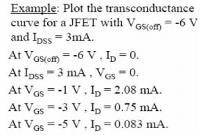
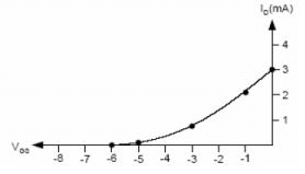
- Plot the point from (3) and connect all the plotted point with a smooth curve.

JFET drain curves
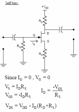
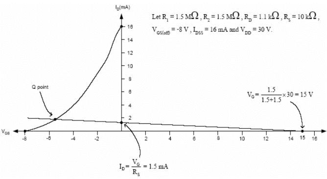
JFET Biasing Circuits
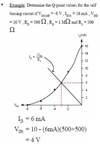
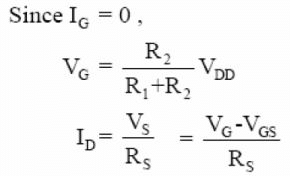
The method used to plot the dc bias line for the voltage-divider bias is as follows:
1. Plot the transconductance curve for the specific JFET.
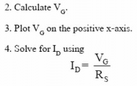
5. Plot ID found in (4) on the y-axis.
6. Extend the line to intersect the transconductance curve to obtain the Q- pomt values.
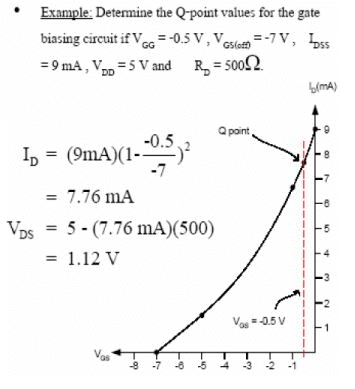
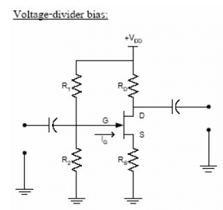
Example: Plot the dc bias line for the voltagedrivers biasing circuit
The document Junction Field Effect Transistor - Semiconductor Devices, CSIR-NET Physical Sciences | Physics for IIT JAM, UGC - NET, CSIR NET is a part of the Physics Course Physics for IIT JAM, UGC - NET, CSIR NET.
All you need of Physics at this link: Physics
FAQs on Junction Field Effect Transistor - Semiconductor Devices, CSIR-NET Physical Sciences - Physics for IIT JAM, UGC - NET, CSIR NET
| 1. What is a junction field effect transistor (JFET)? |  |
Ans. A junction field effect transistor (JFET) is a three-terminal semiconductor device that operates on the principle of controlling the flow of current using an electric field created by a voltage applied across the device. It is commonly used in amplifiers and switching circuits.
| 2. How does a JFET work? | |
Ans. A JFET consists of a channel made of semiconductor material and two regions, called the p-n junctions, on either side of the channel. When a voltage is applied across the p-n junctions, a depletion region is formed in the channel. By applying a control voltage to the gate terminal, the width of the depletion region is controlled, which in turn controls the flow of current through the channel.
| 3. What are the advantages of using JFETs? | |
Ans. JFETs have several advantages, such as low noise, high input impedance, and low power consumption. They also have a wide bandwidth, making them suitable for high-frequency applications. Additionally, JFETs can operate at high temperatures and have a simple structure, making them easy to manufacture.
| 4. What are the different types of JFETs? | |
Ans. There are two main types of JFETs: the n-channel JFET and the p-channel JFET. The n-channel JFET has an n-type channel and two p-type regions, while the p-channel JFET has a p-type channel and two n-type regions. The choice of type depends on the desired polarity of the voltage applied to the terminals.
| 5. How is a JFET different from a bipolar junction transistor (BJT)? | |
Ans. A JFET and a BJT are both types of transistors, but they operate on different principles. While a JFET controls current using an electric field, a BJT controls current using both charge carriers (electrons and holes). JFETs have higher input impedance, lower power consumption, and lower noise compared to BJTs, but BJTs have higher gain and faster switching speeds. The choice between the two depends on the specific application requirements.
Related Exams
About this Document

|
2.6K Views |

|
4.77/5 Rating |

|
Dec 26, 2024 Last updated |
Document Description: Junction Field Effect Transistor - Semiconductor Devices, CSIR-NET Physical Sciences for Physics 2024 is part of Physics for IIT JAM, UGC - NET, CSIR NET preparation.
The notes and questions for Junction Field Effect Transistor - Semiconductor Devices, CSIR-NET Physical Sciences have been prepared according to the Physics exam syllabus. Information about Junction Field Effect Transistor - Semiconductor Devices, CSIR-NET Physical Sciences covers topics
like and Junction Field Effect Transistor - Semiconductor Devices, CSIR-NET Physical Sciences Example, for Physics 2024 Exam. Find important definitions, questions, notes, meanings, examples, exercises and tests below for Junction Field Effect Transistor - Semiconductor Devices, CSIR-NET Physical Sciences.
Introduction of Junction Field Effect Transistor - Semiconductor Devices, CSIR-NET Physical Sciences in English is available as part of our Physics for IIT JAM, UGC - NET, CSIR NET
for Physics & Junction Field Effect Transistor - Semiconductor Devices, CSIR-NET Physical Sciences in Hindi for Physics for IIT JAM, UGC - NET, CSIR NET course.
Download more important topics related with notes, lectures and mock test series for Physics
Exam by signing up for free. Physics: Junction Field Effect Transistor - Semiconductor Devices, CSIR-NET Physical Sciences | Physics for IIT JAM, UGC - NET, CSIR NET
Description
Full syllabus notes, lecture & questions for Junction Field Effect Transistor - Semiconductor Devices, CSIR-NET Physical Sciences | Physics for IIT JAM, UGC - NET, CSIR NET - Physics | Plus excerises question with solution to help you revise complete syllabus for Physics for IIT JAM, UGC - NET, CSIR NET | Best notes, free PDF download
Information about Junction Field Effect Transistor - Semiconductor Devices, CSIR-NET Physical Sciences
In this doc you can find the meaning of Junction Field Effect Transistor - Semiconductor Devices, CSIR-NET Physical Sciences defined & explained in the simplest way possible. Besides explaining types of
Junction Field Effect Transistor - Semiconductor Devices, CSIR-NET Physical Sciences theory, EduRev gives you an ample number of questions to practice Junction Field Effect Transistor - Semiconductor Devices, CSIR-NET Physical Sciences tests, examples and also practice Physics
tests

|
Explore Courses for Physics exam
|
|
Signup for Free!
Signup to see your scores go up within 7 days! Learn & Practice with 1000+ FREE Notes, Videos & Tests.
Related Searches
UGC - NET
,Exam
,CSIR NET
,UGC - NET
,shortcuts and tricks
,Free
,UGC - NET
,video lectures
,past year papers
,Extra Questions
,CSIR-NET Physical Sciences | Physics for IIT JAM
,Summary
,Junction Field Effect Transistor - Semiconductor Devices
,study material
,CSIR NET
,Sample Paper
,Junction Field Effect Transistor - Semiconductor Devices
,MCQs
,Objective type Questions
,CSIR-NET Physical Sciences | Physics for IIT JAM
,mock tests for examination
,Important questions
,CSIR-NET Physical Sciences | Physics for IIT JAM
,Semester Notes
,CSIR NET
,Junction Field Effect Transistor - Semiconductor Devices
,Previous Year Questions with Solutions
,practice quizzes
,Viva Questions
,ppt
;


Additional Information about Junction Field Effect Transistor - Semiconductor Devices, CSIR-NET Physical Sciences for Physics Preparation
Junction Field Effect Transistor - Semiconductor Devices, CSIR-NET Physical Sciences Free PDF Download
The Junction Field Effect Transistor - Semiconductor Devices, CSIR-NET Physical Sciences is an invaluable resource that delves deep into the core of the Physics exam.
These study notes are curated by experts and cover all the essential topics and concepts, making your preparation more efficient and effective.
With the help of these notes, you can grasp complex subjects quickly, revise important points easily,
and reinforce your understanding of key concepts. The study notes are presented in a concise and easy-to-understand manner,
allowing you to optimize your learning process. Whether you're looking for best-recommended books, sample papers, study material,
or toppers' notes, this PDF has got you covered. Download the Junction Field Effect Transistor - Semiconductor Devices, CSIR-NET Physical Sciences now and kickstart your journey towards success in the Physics exam.
Importance of Junction Field Effect Transistor - Semiconductor Devices, CSIR-NET Physical Sciences
The importance of Junction Field Effect Transistor - Semiconductor Devices, CSIR-NET Physical Sciences cannot be overstated, especially for Physics aspirants.
This document holds the key to success in the Physics exam.
It offers a detailed understanding of the concept, providing invaluable insights into the topic.
By knowing the concepts well in advance, students can plan their preparation effectively.
Utilize this indispensable guide for a well-rounded preparation and achieve your desired results.
Junction Field Effect Transistor - Semiconductor Devices, CSIR-NET Physical Sciences Notes
Junction Field Effect Transistor - Semiconductor Devices, CSIR-NET Physical Sciences Notes offer in-depth insights into the specific topic to help you master it with ease.
This comprehensive document covers all aspects related to Junction Field Effect Transistor - Semiconductor Devices, CSIR-NET Physical Sciences.
It includes detailed information about the exam syllabus, recommended books, and study materials for a well-rounded preparation.
Practice papers and question papers enable you to assess your progress effectively.
Additionally, the paper analysis provides valuable tips for tackling the exam strategically.
Access to Toppers' notes gives you an edge in understanding complex concepts.
Whether you're a beginner or aiming for advanced proficiency, Junction Field Effect Transistor - Semiconductor Devices, CSIR-NET Physical Sciences Notes on EduRev are your ultimate resource for success.
Junction Field Effect Transistor - Semiconductor Devices, CSIR-NET Physical Sciences Physics Questions
The "Junction Field Effect Transistor - Semiconductor Devices, CSIR-NET Physical Sciences Physics Questions" guide is a valuable resource for all aspiring students preparing for the
Physics exam. It focuses on providing a wide range of practice questions to help students gauge
their understanding of the exam topics. These questions cover the entire syllabus, ensuring comprehensive preparation.
The guide includes previous years' question papers for students to familiarize themselves with the exam's format and difficulty level.
Additionally, it offers subject-specific question banks, allowing students to focus on weak areas and improve their performance.
Study Junction Field Effect Transistor - Semiconductor Devices, CSIR-NET Physical Sciences on the App
Students of Physics can study Junction Field Effect Transistor - Semiconductor Devices, CSIR-NET Physical Sciences alongwith tests & analysis from the EduRev app,
which will help them while preparing for their exam. Apart from the Junction Field Effect Transistor - Semiconductor Devices, CSIR-NET Physical Sciences,
students can also utilize the EduRev App for other study materials such as previous year question papers, syllabus, important questions, etc.
The EduRev App will make your learning easier as you can access it from anywhere you want.
The content of Junction Field Effect Transistor - Semiconductor Devices, CSIR-NET Physical Sciences is prepared as per the latest Physics syllabus.
|
© EduRev
|
Education Revolution
|


|


Signup to see your scores
go up within 7 days!
Access 1000+ FREE Docs, Videos and Tests
Takes less than 10 seconds to signup