Opto-Electronic Devices - Semiconductor Devices, CSIR-NET Physical Sciences | Physics for IIT JAM, UGC - NET, CSIR NET PDF Download
Optoelectronic devices
P-n junctions are an integral part of several optoelectronic devices. These include photodiodes, solar cells light emitting diodes (LEDs) and semiconductor lasers. In this section, we discuss the principle of operation of these devices and derive equations for key parameters.
Light absorption and emission
A large number of optoelectronic devices consist of a p-type and n-type region, just like a regular p-n diode. The key difference is that there is an additional interaction between the electrons and holes in the semiconductor and light. This interaction is not restricted to optoelectronic devices. Regular diodes are also known to be light sensitive and in some cases also emit light. The key difference is that optoelectronic devices such as photodiodes, solar cells, LEDs and laser diodes are specifically designed to optimize the light absorption and emission, resulting in a high conversion efficiency.
Light absorption and emission in a semiconductor is known to be heavily dependent on the detailed band structure of the semiconductor. Direct bandgap semiconductors, i.e semiconductors for which the minimum of the conduction band occurs at the same wavevector, k, as the maximum of the valence band, have a stronger absorption of light as characterized by a larger absorption coefficient. They are also the favored semiconductors when fabricating light emitting devices. Indirect bandgap semiconductors, i.e. semiconductors for which the minimum of the conduction band does not occur at the same wavevector as the maximum of the valence band, are known to have a smaller absorption coefficient and are rarely used in light emitting devices.
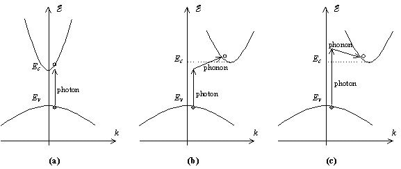
Figure 4.6.1 : E-k diagram illustrating a) Photon absorption in a direct bandgap semiconductor b) Photon absorption in an indirect bandgap semiconductor assisted by phonon absorption and c) Photon absorption in an indirect bandgap semiconductor assisted by phonon emission.
This striking difference is further illustrated with Figure 4.6.1 and can be explained based on the energy and momentum conservation required in the electron-photon interaction. The direct bandgap semiconductor, which has a vertically aligned conduction and valence band, is shown in Figure 4.6.1(a). Absorption of a photon is obtained if an empty state in the conduction band is available for which the energy and momentum equals that of an electron in the valence band plus that of the incident photon. Photons have little momentum relative of their energy since they travel at the speed of light. The electron therefore makes an almost vertical transition on the E-k diagram.
For an indirect bandgap semiconductor, the conduction band is not vertically aligned to the valence band as shown in Figure 4.6.1(b). Therefore a simply interaction of an incident photon with an electron in the valence band will not provide the correct energy and momentum corresponding to that of an empty state in the conduction band. As a result absorption of light requires the help of another particle, namely a photon. Since a phonon, i.e a particle associated with lattice vibrations, has a relatively low velocity close to the speed of sound in the material, it has a small energy and large momentum compared to that of a photon. Conservation of both energy and momentum can therefore be obtained in the absorption process if a phonon is created or an existing phonon participates. The phonon assisted absorption processes are illustrated with Figure 4.6.1(b) and (c). Figure 4.6.1(b) illustrates the absorption of a photon aided by the simultaneous absorption of a phonon, while Figure 4.6.1(c) depicts the absorption of a photon, which results in the emission of a phonon. The minimum photon energy that can be absorbed is slightly below the bandgap energy in the case of phonon absorption and has to be slightly above the bandgap energy in the case of phonon emission. Since the absorption process in an indirect bandgap semiconductor involves a phonon in addition to the electron and photon, the probability of having an interaction take place involving all three particles will be lower than a simple electron-photon interaction in a direct bandgap semiconductor. As a result one finds that absorption is much stronger in a direct bandgap material.
Similarly, in the case of light emission, a direct bandgap material is also more likely to emit a photon than an indirect bandgap material. While indirect bandgap materials are occasionally used for some LEDs, they result in a low conversion efficiency. Direct bandgap materials are used exclusively for semiconductor laser diodes.
Photodiodes
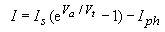
Photodiodes and crystalline solar cells are essentially the same as the p-n diodes, which have been described in this chapter. However, the diode is exposed to light, which yields a photocurrent in addition to the diode current so that the total diode current is given by:
 (4.6.1)
where the additional photocurrent, Iph,is due to photogeneration of electrons and holes shown in Figure 4.6.2.These electrons and holes are pulled into the region where they are majority carriers by the electric field in the depletion region.
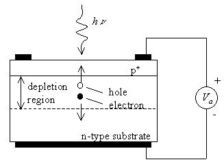
Figure 4.6.2 : Motion of photo-generated carriers in a p-n photodiode.
The photo-generated carriers cause a photocurrent, which opposes the diode current under forward bias. Therefore, the diode can be used as a photodetector - using a reverse or even zero bias voltage - as the measured photocurrent is proportional to the incident light intensity. The diode can also be used as a solar cell - using a forward bias – to generate electrical power.
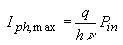
The primary characteristics of a photodiode are the responsivity, the dark current and the bandwidth. The responsivity is the photocurrent divided by the incident optical power. The maximum photocurrent in a photodiode equals
 (4.6.2)
Where Pin is the incident optical power. This maximum photocurrent occurs when each incoming photon creates one electron-hole pair, which contributes to the photocurrent. The maximum photocurrent in the presence of a reflection, R at the surface of the photodiode and an absorption over a thickness d, in a material with an absorption coefficient, a, is given by:
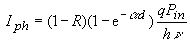 (4.6.3)
This photocurrent is obtained by integrating the generation rate (2.8.12) over the absorption region with thickness, d. The photocurrent is further reduced if photo-generated electron-hole pairs recombine within the photodiode instead of being swept into the regions where they are majority carriers.
The dark current is the current through the diode in the absence of light. This current is due to the ideal diode current, the generation/recombination of carriers in the depletion region and any surface leakage, which occurs in the diode. The dark current obviously limits the minimum power detected by the photodiode, since a photocurrent much smaller than the dark current would be hard to measure.
However, the true limitation is the shot noise generated by the current through the diode. The shot noise as quantified by the average of the square of the noise current is given by:
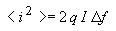 (4.6.4)
Where I is the diode current and Df is the bandwidth of the detector. The bandwidth of the diode is affected by the transit time of the photo-generated carriers through the diode and by the capacitance of the diode. The carrier transit time yields the intrinsic bandwidth of the diode while the capacitance together with the impedance of the amplifier or the transmission line connected to the diode yields a the parasitic RC delay.
Solar cells
Solar cells are typically illuminated with sunlight and are intended to convert the solar energy into electrical energy. The solar energy is in the form of electromagnetic radiation, more specifically "black-body" radiation. The sun’s spectrum is consistent with that of a black body at a temperature of 5800 K. The radiation spectrum has a peak at 0.8 eV. A significant part of the spectrum is in the visible range of the spectrum (400 - 700 nm). The power density is approximately 100 mW/cm2.
Only part of the solar spectrum actually makes it to the earth's surface. Scattering and absorption in the earth's atmosphere, and the incident angle affect the incident power density. Therefore, the available power density depends on the time of the day, the season and the latitude of a specific location.
Of the solar light, which does reach a solar cell, only photons with energy larger than the energy bandgap of the semiconductor generate electron-hole pairs. In addition, one finds that the voltage across the solar cell at the point where it delivers its maximum power is less than the bandgap energy in electron volt. The overall power-conversion efficiency of single-crystalline solar cells ranges from 10 to 30 % yielding 10 to 30 mW/cm2.
The calculation of the maximum power of a solar cell is illustrated by Figure 4.6.3 and Figure 4.6.4. The sign convention of the current and voltage is shown as well. It considers a current coming out of the cell to be positive as it leads to electrical power generation. The power generated depends on the solar cell itself and the load connected to it. As an example, a resistive load is shown in the diagram below.
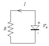
Figure 4.6.3 : Circuit diagram and sign convention of a p-n diode solar cell connected to a resistive load.
The current and the power as function of the forward bias voltage across the diode are shown in Figure 4.6.4 for a photocurrent of 1 mA:
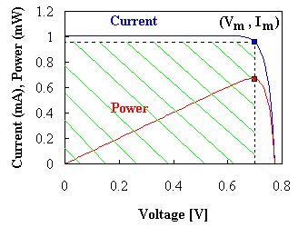
Figure 4.6.4: Current-Voltage (I-V) and Power-Voltage (P-V) characteristics of a p-n diode solar cell with Iph= 1 mA and Is = 10-10 A. The crosshatched area indicates the power generated by the solar cell. The markers indicate the voltage and current, Vm and Im, for which the maximum power, Pm is generated.
We identify the open-circuit voltage, Voc, as the voltage across the illuminated cell at zero current. The short-circuit current, Isc, is the current through the illuminated cell if the voltage across the cell is zero. The short-circuit current is close to the photocurrent while the open-circuit voltage is close to the turn-on voltage of the diode as measured on a current scale similar to that of the photocurrent.
The power equals the product of the diode voltage and current and at first increases linearly with the diode voltage but then rapidly goes to zero as the voltage approaches the turn-on voltage of the diode. The maximum power is obtained at a voltage labeled as Vm with Im being the current at that voltage.
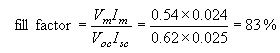
The fill factor of the solar cell is defined as the ratio of the maximum power of the cell to the product of the open-circuit voltage, Voc, and the short-circuit current, Isc, or:
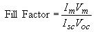 (4.6.5)
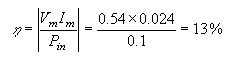
Example 4.6 | A 1 cm2 silicon solar cell has a saturation current of 10-12 A and is illuminated with sunlight yielding a short-circuit photocurrent of 25 mA. Calculate the solar cell efficiency and fill factor. |
Solution |
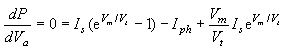
The maximum power is generated for:
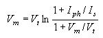
where the voltage, Vm, is the voltage corresponding to the maximum power point. This voltage is obtained by solving the following transcendental equation:
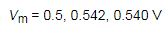
Using iteration and a starting value of 0.5 V one obtains the following successive values for Vm:
and the efficiency equals:
The current, Im, corresponding to the voltage, Vm, was calculated using equation (4.6.1) and the power of the sun was assumed 100 mW/cm2. The fill factor equals:
where the open circuit voltage is calculated using equation (4.6.1) and I = 0. The short circuit current equals the photocurrent. |
LEDs
Light emitting diodes are p-n diodes in which the recombination of electrons and holes yields a photon. This radiative recombination process occurs primarily in direct bandgap semiconductors where the lowest conduction band minimum and the highest valence band maximum occur at k = 0, where k is the wavenumber. Examples of direct bandgap semiconductors are GaAs, InP, and GaN while most group IV semiconductors including Si, Ge and SiC are indirect bandgap semiconductors.
The radiative recombination process is in competition with non-radiative recombination processes such as trap-assisted recombination. Radiative recombination dominates at high minority-carrier densities. Using a quantum well, a thin region with a lower bandgap, positioned at the metallurgical junction, one can obtain high carrier densities at low current densities. These quantum well LEDs have high internal quantum efficiency as almost every electron injected in the quantum well recombines with a hole and yields a photon.
The external quantum efficiency of planar LEDs is much lower than unity due to total internal reflection. As the photons are generated in the semiconductor, which has a high refractive index, only photons traveling normal to the semiconductor-air interface can exit the semiconductor. For GaAs with a refractive index of 3.5, the angle for total internal reflection equals 17o so that only a few percent of the generated photons can escape the semiconductor. This effect can be avoided by having a spherical semiconductor shape, which ensures that most photons travel normal to the interface. The external quantum efficiency can thereby be increased to values larger than 50%.
Laser diodes
Laser diodes are very similar to LEDs since they also consist of a p-n diode with an active region where electrons and holes recombine resulting in light emission. However, a laser diode also contains an optical cavity where stimulated emission takes place. The laser cavity consists of a waveguide terminated on each end by a mirror. As an example, the structure of an edge-emitting laser diode is shown in Figure 4.6.5. Photons, which are emitted into the waveguide, can travel back and forth in this waveguide provided they are reflected at the mirrors.
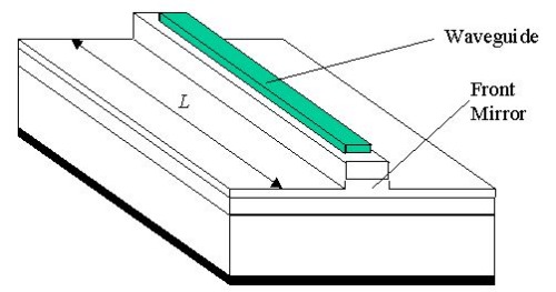
Figure 4.6.5: Structure of an edge-emitting laser diode.
The light in the waveguide is amplified by stimulated emission. Stimulated emission is a process where a photon triggers the radiative recombination of an electron and hole thereby creating an additional photon with the same energy and phase as the incident photon. This process is illustrated with Figure 4.6.6. This "cloning" of photons results in a coherent beam.
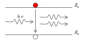
Figure 4.6.6: Stimulated emission of a photon.
The stimulated emission process yields an increase in photons as they travel along the waveguide. Combined with the waveguide losses, stimulated emission yields a net gain per unit length, g. The number of photons can therefore be maintained if the roundtrip amplification in a cavity of length, L, including the partial reflection at the mirrors with reflectivity R1 and R2 equals unity.
This yields the following lasing condition:
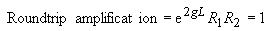 (4.6.6)
If the roundtrip amplification is less than one, then the number of photons steadily decreases. If the roundtrip amplification is larger than one, the number of photons increases as the photons travel back and forth in the cavity. The gain required for lasing therefore equals:
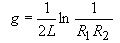 (4.6.7)
Initially, the gain is negative if no current is applied to the laser diode as absorption dominates in the waveguide. As the laser current is increased, the absorption first decreases and the gain increases. The current for which the gain satisfies the lasing condition is the threshold current of the laser, Ith. Below the threshold current very little light is emitted by the laser structure. For an applied current larger than the threshold current, the output power, Pout, increases linearly with the applied current, as each additional incoming electron-hole pair is converted into an additional photon. The output power therefore equals:
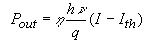 (4.6.8)
where hn is the energy per photon. The factor, h, indicates that only a fraction of the generated photons contribute to the output power of the laser as photons are partially lost through the other mirror and throughout the waveguide.
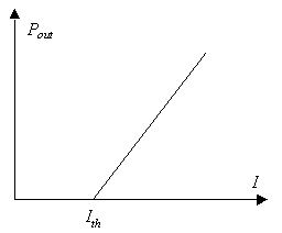
Figure 4.6.7: Output power from a laser diode versus the applied current.
FAQs on Opto-Electronic Devices - Semiconductor Devices, CSIR-NET Physical Sciences - Physics for IIT JAM, UGC - NET, CSIR NET
| 1. What are opto-electronic devices? |  |
| 2. How do semiconductor devices work? | |
| 3. What is the CSIR-NET Physical Sciences exam? | |
| 4. What is the importance of opto-electronic devices in modern technology? | |
| 5. How can one prepare for the CSIR-NET Physical Sciences exam? | |

|
4.68/5 Rating |

|
Dec 26, 2024 Last updated |

|
Explore Courses for Physics exam
|
|
Extra Questions
,CSIR-NET Physical Sciences | Physics for IIT JAM
,CSIR NET
,Sample Paper
,UGC - NET
,Exam
,Opto-Electronic Devices - Semiconductor Devices
,UGC - NET
,video lectures
,CSIR NET
,study material
,Previous Year Questions with Solutions
,Free
,CSIR-NET Physical Sciences | Physics for IIT JAM
,ppt
,past year papers
,practice quizzes
,CSIR-NET Physical Sciences | Physics for IIT JAM
,Viva Questions
,Summary
,CSIR NET
,Opto-Electronic Devices - Semiconductor Devices
,mock tests for examination
,Semester Notes
,Opto-Electronic Devices - Semiconductor Devices
,UGC - NET
,Objective type Questions
,Important questions
,shortcuts and tricks
,MCQs
;


Opto-Electronic Devices - Semiconductor Devices, CSIR-NET Physical Sciences Free PDF Download
Importance of Opto-Electronic Devices - Semiconductor Devices, CSIR-NET Physical Sciences
Opto-Electronic Devices - Semiconductor Devices, CSIR-NET Physical Sciences Notes
Opto-Electronic Devices - Semiconductor Devices, CSIR-NET Physical Sciences Physics Questions
Study Opto-Electronic Devices - Semiconductor Devices, CSIR-NET Physical Sciences on the App
|
© EduRev
|
Education Revolution
|


|


