Semiconductors Electronics: Materials, Devices And Simple Circuits | Physics Class 12 - NEET PDF Download
Introduction
- The foundation for the growth and progress of modern solid-state semiconductor electronics dates back to the 1930s.
- During this time, it was discovered that certain semiconductors and their junctions can control how many charge carriers flow through them and in which direction.
- By using simple methods like light, heat, or a small applied voltage, we can change the number of moving charge carriers in a semiconductor.
- In these devices, the supply and movement of charge carriers happen within the solid material itself.
- There is no need for a vacuum or external heating to operate these devices.
- As a result, these devices are:
- Compact in size
- Energy-efficient with low power consumption
- Low-voltage operation
- Long-lasting with high reliability
Classification Of Metals, Conductors And Semiconductors
On the basis of conductivity
The conductivity of a material indicates whether they can be classified as metals, semiconductors or insulators.
- The electrical conductivity is expressed as σ whereas the reciprocal of conductivity is resistivity ρ = 1/σ.
- Metals – Metals have high conductivity and low resistivity ; ρ is of order10-2 to 10-8 Ω m ; σ is of order 102 to 108 S/m
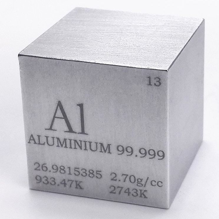 Aluminium Metal
 - Semiconductors – They have conductivity and resistivity in between metals and insulators ; ρ is of order 10-5 to 10-6 Ω m ; σ is of order 105 to 106 S/m
- Insulators – They have high resistivity and hence low conductivity ; ρ is of order 10-11 to 10-19 Ω m ; σ is of order 102 to 1019 S/m

Classification of Semiconductors
The semiconductors can be classified into:
(a) Element semiconductors
(b) Compound semiconductors
(a) Element semiconductors – These type of semiconductors are available in natural form like Silicon (Si) and germanium (Ge)
(b) Compound semiconductors – When semiconductors are made by compounding the metals, we get compound type semiconductor.
They can be further classified into
• Inorganic semiconductors like CdS, GaAs etc.
• Organic semiconductors like Antracene, doped pthalocyanines
• Organic polymers – Polypyrrole, polyaniline, polythiophene, etc.
Band Theory of Solids
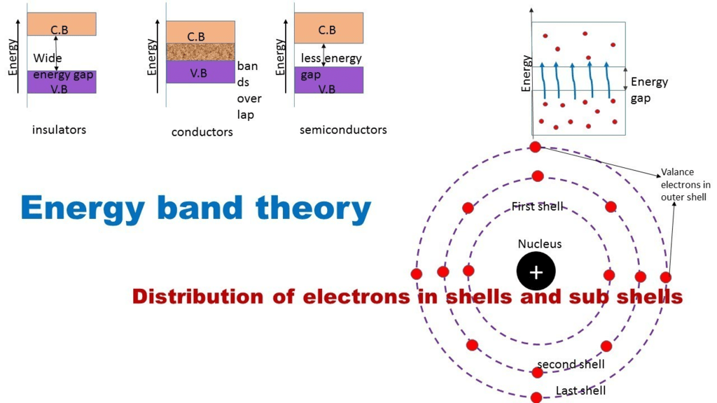
In a substance, as many atoms are close to each other, the energy levels of the atom form a continuous band, wherein the electrons move. This is called the band theory of solids.
- We know that in an atom, the protons and the neutrons constitute the central part called the nucleus.
- The electrons revolve around the nucleus in defined orbits.
- The orbits are named as 1s, 2s, 2p, 3s, 3p, 3d etc. each of which has a discrete energy level.
- All electrons in the same orbit have the same energy.
- The electrons in the innermost orbits which are completely filled constitute the valence electrons whereas the electrons in the outermost orbit which do not completely fill that shell are called conduction electrons.
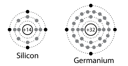
- As seen in the diagram below, both Si and Ge have 4 electrons in the outermost shell.
- When in the crystal, the atoms are close to each other and hence they may be the flow of electrons from one atom to another in the conduction band.
Let us discuss in detail by considering interatomic distance in the X-axis and energy in the Y-axis:
As seen in the diagram below, the graph is divided into 4 regions – Region A, B, C and D.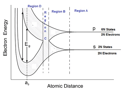
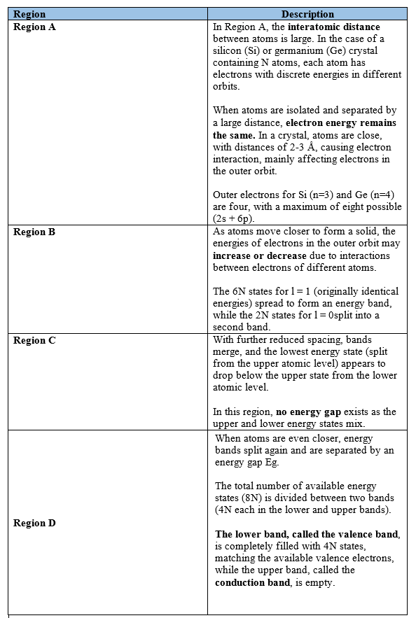
Three Types of Energy Bands in A Solid
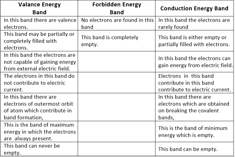
- Valence energy band
- Conduction energy band
- Forbidden energy gap.
Table: Difference between valence, forbidden and conduction energy bands
More about Energy Bands
- The conduction band is also known as the first permitted energy band or first band.
- As there are energy levels f electrons in an atom, similarly there are three specific energy bands for the electrons in the crystal formed by these atoms as shown in the figure.
- Completely filled energy bands: The energy band, in which the maximum possible number of electrons are present according to capacity is known as completely filled bank.
- Partially filled energy bands: The energy band, in which a number of electrons present is less than the capacity of the band, is known as a partially filled energy band.
- Electric conduction is possible only in those solids which have an empty energy band or partially filled energy band.
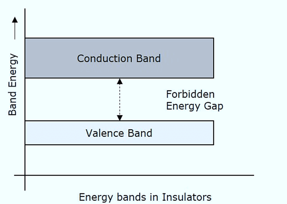
- Energy gap or Band gap (Eg): The minimum energy which is necessary for shifting electrons from valence band to conduction band is defined as band gap (Eg).
- The forbidden energy gap between the valence band and the conduction band is known as band gap (Eg). i.e. Eg = Ec – Ev.
Classification on the basis of energy bands
Depending upon the relative position of the valence band and the conduction band, the solids can be classified into conductors, insulators and semiconductors.
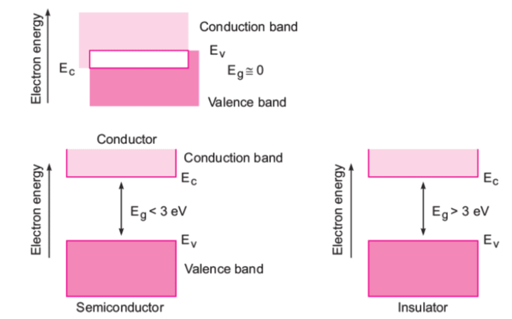
Conductors
- The conduction band and the valence band partly overlap each other and there is no forbidden energy band gap in between.
- The electrons from the valence band can easily move into the conduction band.
- Hence, a large number of electrons are available for conduction.
- The resistance of such materials is low and conductivity is high.
Insulators
- In case of insulators, a large energy gap exists between the valence band and the conduction band.
- The energy gap is so high that the electrons from the valence band cannot move to the conduction band by thermal excitation.
- As there are no electrons in the conduction band, electrical conduction is not possible.
Semiconductors
- A finite but a small energy gap exists between the valence band and the conduction band.
- At room temperature, some of the electrons from the valence band acquire energy and move into the conduction band.
- Hence, at high temperature, semiconductors have conductivity and resistance is also not as high as insulators.
- There are two types – Intrinsic semiconductor and Extrinsic semiconductor.
Table: Difference between Conductors, Semi-conductors and Insulators.
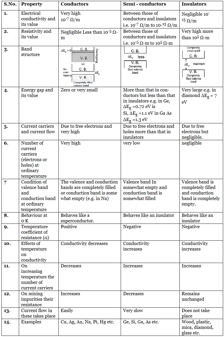
Semiconductors are the materials that have a conductivity between conductors (generally metals) and non-conductors or insulators (such as ceramics).
Semiconductors can be compounds such as gallium arsenide or pure elements, such as germanium or silicon. Physics explains the theories, properties and mathematical approach governing semiconductors.
Properties of Semiconductors
- Semiconducting elements are tetra-valent i.e. there are four electrons in their outermost orbit.
- Their lattice is face centered cubic (F.C.C.)
- The number of electrons or cotters is given by
i.e. on increasing temperature, the number of current carriers increases. - There are uncharged.
- Semiconductor acts like an insulator at Zero Kelvin. On increasing the temperature, it works as a conductor.
- Due to their exceptional electrical properties, semiconductors can be modified by doping to make semiconductor devices suitable for energy conversion, switches, and amplifiers.
- Lesser power losses.
- Semiconductors are smaller in size and possess less weight.
- Their resistivity is higher than conductors but lesser than insulators.
- The resistance of semiconductor materials decreases with the increase in temperature and vice-versa.
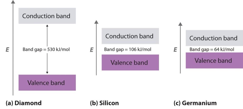
Example of different semi-conductors
- Holes or cotters
(i) The deficiency of electrons in covalent band formation in the valence band in defined as hole or cotter,
(ii) These are positively charged. The value of positive charge on them is equal to the electron charge.
(iii) Their effective mass is less than that of electrons.
(iv) In an external electric field, holes move in a direction opposite to that of electrons i,e. they move from positive to negative terminal.
(v) They contribute to current flow.
(vi) Holes are produced when covalent bonds in valence band break.
Transfer of electrons from valence band to conduction band
Types of Semiconductor
Semiconductors can be classified as:
- Intrinsic Semiconductor
- Extrinsic Semiconductor

Intrinsic Semiconductor
- An intrinsic type of semiconductor material is made to be very pure chemically. It is made up of only a single type of element.
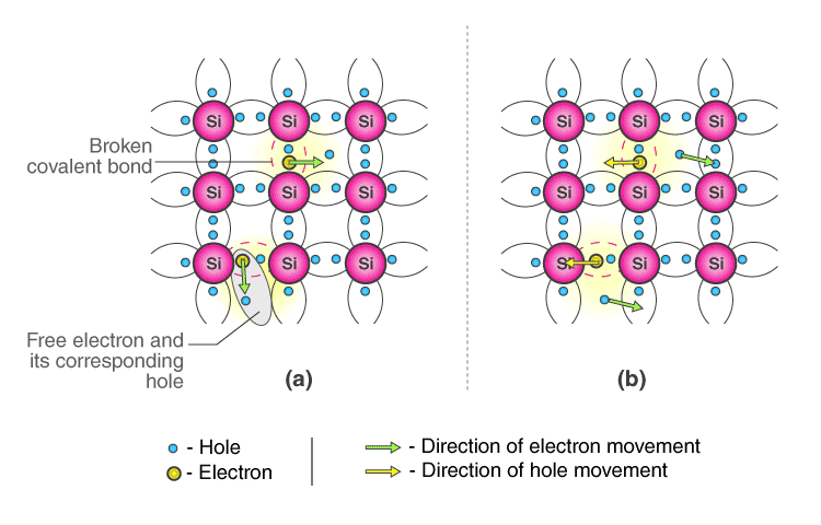 Conduction Mechanism in Case of Intrinsic Semiconductors (a) In absence of electric field (b) In presence of electric Field
- Germanium (Ge) and Silicon (Si) are the most common type of intrinsic semiconductor elements. They have four valence electrons (tetravalent). They are bound to the atom by covalent bond at absolute zero temperature.
- When the temperature rises, due to collisions, few electrons are unbounded and become free to move through the lattice, thus creating an absence in its original position (hole). These free electrons and holes contribute to the conduction of electricity in the semiconductor. The negative and positive charge carriers are equal in number.
- The thermal energy is capable of ionizing a few atoms in the lattice, and hence their conductivity is less.
➢ The Lattice of Pure Silicon Semiconductor at Different Temperatures
- At absolute zero Kelvin temperature: At this temperature, the covalent bonds are very strong and there are no free electrons and the semiconductor behaves as a perfect insulator.
- Above absolute temperature: With the increase in temperature few valence electrons jump into the conduction band and hence it behaves like a poor conductor.
➢ Energy Band Diagram of Intrinsic Semiconductor
- The energy band diagram of an intrinsic semiconductor is shown below:
 (a) Intrinsic Semiconductor at T = 0 Kelvin, behaves like an insulator (b) At t>0, four thermally generated electron pairs
 - In intrinsic semiconductors, current flows due to the motion of free electrons as well as holes. The total current is the sum of the electron current Ie due to thermally generated electrons and the hole current Ih
Total Current (I) = Ie + Ih - For an intrinsic semiconductor, at finite temperature, the probability of electrons to exist in conduction band decreases exponentially with increasing bandgap (Eg)

Where,
Eg = Energy bandgap
Kb = Boltzmann’s constants
Extrinsic Semiconductor
- The conductivity of semiconductors can be greatly improved by introducing a small number of suitable replacement atoms called impurities.

- The process of adding impurity atoms to the pure semiconductor is called doping.
- Usually, only 1 atom in 107 is replaced by a dopant atom in the doped semiconductor.
- An extrinsic semiconductor can be further classified into:
(i) N-type Semiconductor
(ii) P-type Semiconductor
Table: Difference between intrinsic and extrinsic semiconductors
S.No. | Intrinsic semiconductors | Extrinsic semiconductors |
1. | Pure Ge or Si is known as intrinsic semiconductor | The semiconductor, resulting from mixing impurity in it, is known as extrinsic semiconductors. |
2. | Their conductivity is low (because only one electron in 109 contribute) | Their conductivity is high |
3. | The number of free electrons (m in conduction band Is equal to the number of holes pi in valence band.) | In these ni ≠pi |
4. | These are not practically used | These are practically used |
5. | In these the energy gap is very small | In these the energy gap is more than that in pure semiconductors. |
6. | In these the Fermi energy level lies in the middle of valence band and conduction | In these the Fermi level shifts towards valence or conduction energy bands. |
➢ Properties of Extrinsic Semiconductors
- At absolute zero temperature (0 K) there are no free electrons in them.
- At room temperature, the electron-hole pair in sufficient number are produced.
- Electric conduction takes place via both electrons and holes.
- The drift velocities of electrons and holes are different.
- The drift velocity of electrons (Vdn) is greater than that of holes (Vdp).
- The total current is I = In + Jp.
- In connecting wires the current flows only via electrons.
- The current density is given by:
Where Vdn = drift velocity of electrons
μn = mobility of electrons
Vdp = drift velocity of holes
μp = mobility of holes - The electric conductivity is given by s = nq(mn + mp).
- Mobility of electron mn = Vdn / E.
- Mobility of holes mp = Vdp/E.
- At room temperature sGe > sSi because nGe > nSi
where nGe = 2.5' 1013/cm3 and nSi = 1.4' 1010 /cm3.
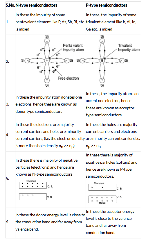
N-Type Semiconductor

- Mainly due to electrons
- Entirely neutral
- I = Ih and nh >> ne
- Majority – Electrons and Minority – Holes
- When a pure semiconductor (Silicon or Germanium) is doped by pentavalent impurity (P, As, Sb, Bi) then, four electrons out of five valence electrons bonds with the four electrons of Ge or Si.
- The fifth electron of the dopant is set free. Thus, the impurity atom donates a free electron for conduction in the lattice and is called “Donar“.
- Since the number of free electron increases by the addition of an impurity, the negative charge carriers increase. Hence, it is called n-type semiconductor.
- Crystal as a whole is neutral, but the donor atom becomes an immobile positive ion. As conduction is due to a large number of free electrons, the electrons in the n-type semiconductor are the majority carriers and holes are the majority carriers.
P-Type Semiconductor

- Mainly due to holes
- Entirely neutral
- I = Ih and nh >> ne
- Majority – Holes and Minority – Electrons
- When a pure semiconductor is doped with a trivalent impurity (B, Al, In, Ga ) then, the three valence electrons of the impurity bonds with three of the four valence electrons of the semiconductor.
- This leaves an absence of electron (hole) in the impurity. These impurity atoms which are ready to accept bonded electrons are called “Acceptors“.
- With the increase in the number of impurities, holes (the positive charge carriers) are increased. Hence, it is called p-type semiconductor.
- Crystal as a whole is neutral, but the acceptors become an immobile negative ion. As conduction is due to a large number of holes, the holes in the p-type semiconductor are majority carriers and electrons are majority carriers.
Table: Difference between N-type and P-type semiconductors
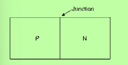
P-n Junction Formation
(a) The device formed by joining atomically a wafer of P-type semiconductor to the wafer of N-type semiconductor is known as P-n junction.
(b)There are three processes of making junctions
(i) Diffusion
(ii) Alloying
(iii) Growth
In majority of cases P-N junction is formed by diffusion process. The impurity concentration is maximum at surface and decreases gradually inside the semiconductor.
(c) Conduction of current in P-N Junction:
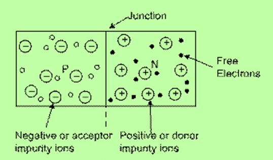
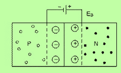
(i) In P-N junction the majority cotters in P-region and majority electrons in N-region start diffusing due to concentration gradient and thermal disturbance towards N-region and P-region respectively and combine respectively with electrons and cotters and become neutral.
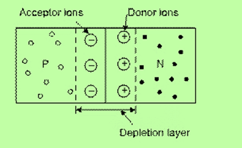
(ii) In this process of neutralization there occurs deficiency of free current carriers near the junction and layers of positive ions in N-region and negative ions in P-region are formed. These ions are immobile.
(iii) Due to this an imaginary battery or internal electric field is formed at the junction which is directed from N to P.
- The region on both sides of P-N junction in which there is deficiency of free current carriers, is known as the depletion layer.
- Its thickness is of the order of 1 micro m (= 10–6)
- On two sides of it, there are ions of opposite nature. i.e. donor ion (+ve) on N-side and acceptor ions (–ve) on P-side.
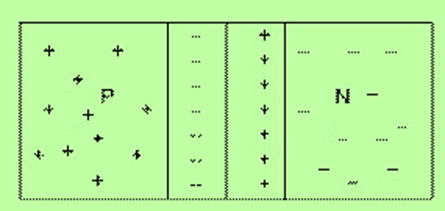
- This stops the free current carriers to crossover the junction and consequently a potential barrier is formed at the junction.
- The potential difference between the ends of this layer is defined as the contact potential or potential barrier (VB).
- The value of VB is from 0.1 to 0.7 volt which depends on the temperature of the junction. It also depends on the nature of semiconductor and the doping concentration. For germanium and silicon its values are 0.3 V and 0.7 V respectively.
- Symbolic representation of diode:

- The direction of current flow is represented by the arrow head.
- In equilibrium state current does not flow in the junction diode.
- In can be presumed to be equivalent to a condenser in which the depletion layer acts as a dielectric.

- Potential distance curve at P-N Junction

- Charge density curve at P-N Junction

- Curve between electric field and distance near P-N junction

P-n Junction Diode
- A semiconductor diode is a p-n junction with metallic contacts provided at the ends for the application of an external voltage
- Thus p-n junction diode is a two terminal device represented as

- The equilibrium potential barrier can be altered by applying an external voltage V across the diode.
There are two methods of biasing a p-n unction – Forward bias and reverse bias.
Forward biasing
- If the positive terminal of the external battery is connected to the p-side and the negative terminal of the external battery is connected to the n-side, then the p-n junction is said to be forward biased.

- The direction of the applied voltage V is in a direction opposite to that of the potential barrier setup at the junction.

- As a result of this, the depletion layer width decreases and the barrier height is reduced. The effective barrier height under forward bias is VB – V.
- If the applied voltage V is small, the barrier potential will be reduced only slightly below the equilibrium value. Hence, only small number carriers will possess energy to cross the junction. Thus, the current is small.
- If the applied voltage V is large, the barrier potential will be reduced significantly. Hence, the current is significant.
- Due to the applied voltage, the electrons from the n-side cross the depletion region and reach the p-side. Similarly, the holes from the p-side reach the n-side.
- As electrons reach the p-side and electrons are minority carriers in p-region, the forward bias is also known as minority carrier injection.
- At the junction, the minority carrier concentration increases significantly.
- Due to concentration gradient, the injected electrons on p-side diffuse from the junction edge of p-side to the other end of the p-side.
- Similarly, the injected holes on the n-side diffuse from the junction edge of n-side to the other end of n-side.
- The motion of charged carriers on either side gives rise to current and is usually measured in mA.
- The total diode forward current is sum of hole diffusion current and conventional current due to electron diffusion.
Reverse biasing
- If the positive terminal of the external battery is connected to the n-side and the negative terminal of the external battery is connected to the p-side, then the p-n junction is said to be reverse biased

- The direction of the applied voltage is same as that of the barrier potential.
- As a result, the barrier height increases and the depletion region widens due to change in electric field.
- The effective barrier height is VB + V.
- This suppresses the flow of electrons from n region to p region and holes from the p region to n region. Hence, diffusion current decreases.
- The electric field direction of the junction is such that if electrons on p-side or holes on n-side in their random motion come close to the junction, they will be swept to its majority zone. This gives rise to drift current of order of few µA.
- The diode reverse current is not much dependent on the applied voltage. Even a small voltage is sufficient to sweep the minority carriers from one side of the junction to the other side of the junction.
- The current under reverse bias is essentially voltage independent up to a critical reverse bias voltage, known as breakdown voltage VBE.
- When V = VBE, the diode reverse current increases sharply. If the current is not limited, the p-n junction will get destroyed.
|
74 videos|314 docs|88 tests
|
FAQs on Semiconductors Electronics: Materials, Devices And Simple Circuits - Physics Class 12 - NEET
| 1. What are the main differences between conductors, semiconductors, and insulators based on band theory? |  |
| 2. What are intrinsic and extrinsic semiconductors, and how do they differ? |  |
| 3. How is a P-N junction formed, and why is it important in semiconductor technology? |  |
| 4. What is the function of a P-N junction diode in electronic circuits? |  |
| 5. What are some common applications of semiconductor materials in electronics? |  |


