Semiconductors - 2 | Electronic Devices - Electronics and Communication Engineering (ECE) PDF Download
Hall Effect
When a magnetic field is applied to a current-carrying conductor in a direction perpendicular to that of the flow of current, a potential difference or transverse electric field is created across a conductor. This phenomenon is known as the Hall Effect.
According to this effect the statements are:
If a specimen (metal or semiconductor) carrying a current I is placed in a transverse magnetic field B, an electric field E is induced in the direction perpendicular to both I and B. This phenomenon, known as the Hall effect, is used to determine whether a semiconductor is n- or p-type and to find the carrier concentration. Also, by simultaneously measuring the conductivity σ, the mobility μ can be calculated.
Consider the figure shown below. Here current l is in +x-direction, magnetic field B is in +z direction then induced electric field will be in negative y-direction.
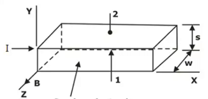 Semiconductor Bar
Hence a force will be exerted in the negative y-direction on the current carriers.
The current l may be due to holes moving from left to right or to free electrons travelling from right to left in the semiconductor specimen. Hence, independently of whether the carriers are holes or electrons, they will be forced downward toward side 1 of above figure.
If the semiconductor is n-type material, so that the current is carried by the electrons, these electrons will accumulate on side 1, and this surface becomes negativity charged with respect to side 2. Hence a potential, called the Hall voltage, appears between surface 1 and 2.
Now under the equilibrium condition
qE = Bvq
But, E = VH/d and j = vρ = I/wd
Combining these relationships, we find
Vh = Ed = Bvd = Bjd/ρ = BI/ρw
Where ρ is the charge density, w is the width of the specimen and d is the distance between surfaces 1 and 2.
It is customary to introduce the Hall coefficient RH defined by
RH = 1/ρ
Hence, Rh = VHw/BI
By hall experiment mobility of charge carriers is given as
μ = 8/3π σRH
or, μ ≅ σRH
⇒ Hall coefficient, RH Temperature coefficient of resistance of given specimen.
⇒ For metals, σ is larger, VH is small.
⇒ For semiconductors, σ is small, VH is large.
Hall Effect in an n-type semiconductor
- If the magnetic field is applied to an n-type semiconductor, both free electrons and holes are pushed down towards the bottom surface of the n-type semiconductor. Since the holes are negligible in n-type semiconductor, so free electrons are mostly accumulated at the bottom surface of the n-type semiconductor.
- This produces a negative charge on the bottom surface with an equal amount of positive charge on the upper surface. So in n-type semiconductor, the bottom surface is negatively charged and the upper surface is positively charged.
- As a result, the potential difference is developed between the upper and bottom surface of the n-type semiconductor. In the n-type semiconductor, the electric field is primarily produced due to the negatively charged free electrons. So the hall voltage produced in the n-type semiconductor is negative.
Hall Effect in a p-type semiconductor
- If the magnetic field is applied to a p-type semiconductor, the majority carriers (holes) and the minority carriers (free electrons) are pushed down towards the bottom surface of the p-type semiconductor. In the p-type semiconductor, free electrons are negligible. So holes are mostly accumulated at the bottom surface of the p-type semiconductor.
- So in the p-type semiconductor, the bottom surface is positively charged and the upper surface is negatively charged.
- As a result, the potential difference is developed between the upper and bottom surface of the p-type semiconductor. In the p-type semiconductor, the electric field is primarily produced due to the positively charged holes. So the hall voltage produced in the p-type semiconductor is positive. This leads to the fact that the produced electric field is having a direction in the positive y-direction.
Hall voltage
The expression for the Hall voltage is given by:
VH = IB/qnd
Applications of Hall Effect
- Measurement of magnetic flux density.
- Measurement of displacement.
- Measurement of current.
- Measurement of power in Electro-Magnetic waves.
- Determination of mobility of semiconductor material.
Hall effect is used in many applications as following:
[Note: Minority carrier mobility (μ) and diffusion coefficient(D) can be measured independently with the help of Haynes-Shockley experiment.]
Solved Example
Example 1: A n type Ge Sample has a donor density ND = 1021 atoms/m3. It is arranged in a Hall experiment having a magnetic field B = 0.2 Wb/m2 and current density J = 500 A/m2. Find the hall voltage generated when the thickness of sample is 2 mm. Also calculate the field intensity induced in magnitude ?
Solution: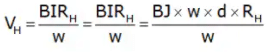
VH = BJDRH
VH = 0.2 x 500 x 2 x 10-3 x 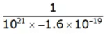
⇒ VH = 1.25mV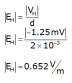
Fermi Level in Intrinsic and Extrinsic Semiconductors
- Electrons in solids obey Fermi-Dirac statistics. The distribution of electrons over a range of allowed energy levels at thermal equilibrium is:

Where k s Boltzmann’s constant (k = 8.62 × 10⁻⁵ eV/K = 1.38 × 10⁻²³ J/K). - The function f(E), the Fermi-Dirac distribution function, gives the probability that an available energy state of E will be occupied by an electron at absolute temperature T. The quantity EF is called the Fermi level.
- If E = EF then = 0.5 or 50%
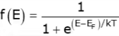
If E > EF then f(E) < ½
If E > EF then f(E) > ½
A closer examination of f(E) indicates that at 0 K the distribution takes the simple rectangular form shown in figure. At temperature higher than 0K, some probability exists for states above the Fermi level to be filled.
Fermi Level in Intrinsic Semiconductor
In intrinsic semiconductor Fermi level EF is given by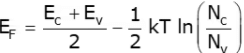
where, NC = density of states in conduction band
Nv = density of states in valence band
In pure Semiconductor at T = 0K, Fermi level lies in the middle of bandgap.
Fermi Level in n-type Semiconductor
Fermi level in n-type semiconductor is given by
EF = Ec - kT In (Nc/Nd)
Where, ND = doping concentration.
- Fermi level in n-type semiconductor depends on temperature as well as on doping concentration.
- At 0K Fermi level coincides with that of lowest energy level of conduction band.
- As doping increases Fermi level moves towards conduction band.
- Shift in Fermi level in n-type semiconductor with respect to Fermi level of intrinsic semiconductor is
shift = kT
shift ≅ kT
Fermi Level in p-type Semiconductor
Fermi level in p-type semiconductor is given by
Ef = Ev + kT in (Nv/NA)
- In p-type semiconductor Fermi level depends on both temperature as well as on doping concentration NA.
- As temperature increases Fermi level moves away from EV i.e. towards middle of band gap.
- As 0K Fermi level coincides with highest energy level EV of valence band.
- As doping concentration increases Fermi level moves toward EV or away of middle of band gap
- Shift in Fermi level in p-type semiconductor with respect to Fermi level of intrinsic semiconductor as
shift = kT
shift ≅ kT
Solved Example
Example 1: If the Fermi energy in silicon is 0.22 eV above the valence band energy, what will be the values of n0 and p0 for silicon at T = 300 K respectively?
Solution: Given that Fermi energy in silicon is 0.22 eV above the valence band energy, i.e.
EF – Ev = 0.22 eV
So, we obtain the hole concentration as
p0 = Nv exp
= 1.04 x 10¹⁹ exp 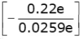
= 2.13 x 1015cm-3
Now, the energy bandgap for silicon is 1.12 eV, i.e.
Eg = Ec – Ev = 1.12 eV
Therefore, we obtain
Hence, the hole concentration is
n0 = Nc exp
= 2.8 x 10¹⁹ exp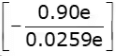
= 2.27 x 104 cm-3
|
21 docs|29 tests
|
FAQs on Semiconductors - 2 - Electronic Devices - Electronics and Communication Engineering (ECE)
| 1. What is the Hall Effect? |  |
| 2. What is the Fermi Level in intrinsic semiconductors? | |
| 3. What is the Fermi Level in extrinsic semiconductors? | |
| 4. How does the Hall Effect help in determining the type of charge carriers in a semiconductor? | |
| 5. How does doping affect the Fermi Level in a semiconductor? | |

|
4.72/5 Rating |

|
Dec 22, 2024 Last updated |

|
Explore Courses for Electronics and Communication Engineering (ECE) exam
|
|
MCQs
,Semiconductors - 2 | Electronic Devices - Electronics and Communication Engineering (ECE)
,Exam
,Semiconductors - 2 | Electronic Devices - Electronics and Communication Engineering (ECE)
,Extra Questions
,Important questions
,past year papers
,practice quizzes
,Sample Paper
,mock tests for examination
,video lectures
,study material
,ppt
,Summary
,Viva Questions
,Semester Notes
,Free
,Objective type Questions
,Semiconductors - 2 | Electronic Devices - Electronics and Communication Engineering (ECE)
,Previous Year Questions with Solutions
,shortcuts and tricks
;


Semiconductors - 2 Free PDF Download
Importance of Semiconductors - 2
Semiconductors - 2 Notes
Semiconductors - 2 Electronics and Communication Engineering (ECE) Questions
Study Semiconductors - 2 on the App
|
© EduRev
|
Education Revolution
|


|


