Circuits Analysis & Applications of Diodes, BJT, FET & MOSFET - 2 | Analog Circuits - Electronics and Communication Engineering (ECE) PDF Download
In this article, We are providing the 2nd part of the study notes on Circuits Analysis and Applications of Diodes, BJT, and MOSFET for GATE and other Electrical Engineering exams. The study notes cover the topic such as Analysis of the operating mode of BJT, Operating Point, DC and AC load line, Instability in collector current and BJT Biasing.
Table of Content
➤ ANALYSIS OF OPERATING MODE OF BJT
Method-1
To determine the mode of operation of a BJT, the following steps are followed.
- Step 1 :- Let Assume that the transistor is biased on the forward active mode,
In this case put
VBE = VBE(ON), IB > 0 and IC = βIB - Step 2 :- Evaluate the linear circuit with these assumption.
- Step 3 :- Find the each terminal voltages i.e., VB, VC and VE.
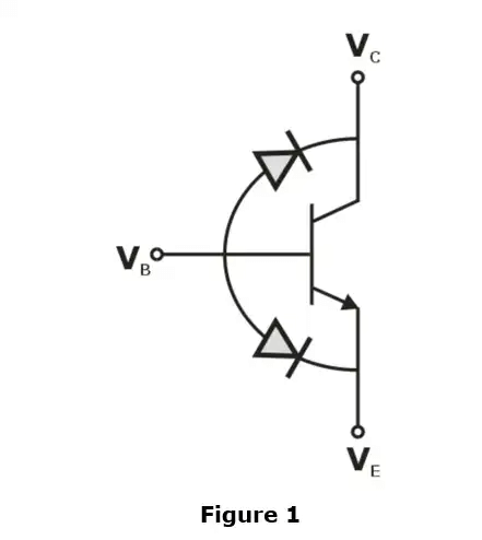
- Step 4 :- Now, the BJT can be considered as two diodes connected back to back as shown below in figure 1

- Step 5 :- Inspect whether the diodes are forward biased or reverse biased
- Step 6 :- Conclude the operating mode of transistor for the condition according given in table 1.

Method-2
The mode of operation of the Transistor is found by follwing the given steps.
- Step 1 :- Assume the transistor is biased in the forward active mode. In this case put
VBE = VBE(ON), IB>0 and IC = βIB - Step 2 :- Evaluate the linear circuit with these assumption.
- Step 3 :- Determine the operating region by following condition
VCE > VCE (sat) Active region
VCE < VCE (sat) saturation region
Method-3
To determine the mode of operation of a BJT, the following steps are followed.
- Step 1 :- Assume the transistor is biased in the forward active region. In this case put
VBE = VBE(ON), IB > 0 and IC = βIB - Step 2 :- Determine the collector current, (IC)active for the transistor operating in active region.
- Step 3 :- Determine the value of collector current (IC)sat in saturation mode.
- Step 4 :- Find the mode of operation by following the given below conditions.
(IC)sat < (IC)active Saturation
(IC)sat > (IC)active Active
➤ OPERATING POINT
- From transistor characteristics, it is clear that a transistor functions most linearly when it is constrained to operate in its active region.
- To establish an operating point in the region it is necessary to provide approximate direct potentials and current, using external source.
- Once an operating point (also known as Quiescent or Q-point) is established, time varying excursions of input signal (base current, for example) should cause an output signal (Collector voltage as collector current) of the same waveform.
- If the output signal is not faithful reproduction of the input signal, for example, it is clipped on one side, then the operating point is unsatisfactory and should be relocated on the collector characteristics.
- Figure 3(a) shows the common emitter circuit (the capacitors have negligible reactance at the lowest frequency of operation of this circuit). Figure 3(b) gives the output characteristics of the transistor used in figure 3(a).
- Note that even if there are freedom to choose RC, RL, Rb and VCC, it is not possible to operate the transistor everywhere in active region because various transistor ratings limit the range of useful operation.


➤ THE DC AND AC LOAD LINES
The capacitance considered in the circuit of figure 3(a) is large enough so that they act as open circuits under DC conditions but short circuits at the lowest frequency of operation of the circuit. Since the capacitor are open-circuited under DC conditions so the circuit can be redrawn as shown below in figure 3(c)

 .....(i)
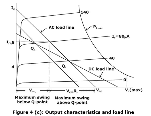
- Equation (i) represents the dc or static load line of the circuit with a slope of –1/RC as drawn in figure 3(b).
- If RL = ∞ and if the input signal (base current) is large and symmetrical, operating point Q1 must be located at the center of the load line. In this way, the collector voltage and current may vary approximately symmetrical around the quiescent values VC and IC, respectively.
- If RL ≠ ∞, however, an ac or dynamic load line must be considered.
- Since capacitors act as short circuits at input signal frequency, the effective load at the collector becomes RC in parallel with RL.
- Now, AC or dynamic load line is defined as a line that passes through the dc operating point Q1 and has a slope equal to 1/R'L corresponding to the collector load. =RC||RL, Under AC conditions. This AC load line is indicated in figure 3(b).
➤ INSTABILITY IN COLLECTOR CURRENT
From the above discussion, it is found that to obtain faithful reproduction of the input signal it should necessary to maintain a stable Q-point.
The collection current can be calculated by the following equation.
Ic = β IB + (1+β) Ico …………(ii)
From equation (ii), It can be concluded that Ic is unstable due to the following reasons:
- Variations in Ico
Ico is the reverse saturation current of the collection function. It increases with an increase in temperature because of the increase in the concentration of minority carriers.
(i) If temperature increase by 1°C then Ico increases by 7%.
(ii) For each 10°c rise in temperature Ico
Hence it is observed that variation in temperature causes change in Ico and as result, Ic also varies. - Variation in VBE
When temp increased 1°C, VBE decreased by 2.5 mV.
Hence, changes in temperature create change in VBE due to which base current (IB) changes. Hence from equ. (ii) it can be concluded that collection current Ic also varies. - Variation in β
β varies w.r.t transistor replacement or due to variation in temperature.
(i) When a transistor is replaced with another transistor, β value will vary because it is practically difficult to find two transistors having exactly same value of β.
(ii) For a given transistor, β also increases with an increase in temperature.
Hence from the above discussion, it can be concluded that Ic is unstable due to variation in Ico, β and VBE i.e
Ic = f (ICO, VBE, β) …………(iii)
From the above equation, It is clear that Ic is a function of Ico, β and VBE.
By Applying partial differentiation on equation (iii),
ΔIc = s.ΔIco + s’ΔVBE + s”Δβ ………….(iv)
Where s, s’ and s” are stability factors.
- From equation (iv), it can be conducted that for greater stability in Ic, ΔIc should be smaller, which is possible when stability factors are smaller.
- Instability in Ic has two undesired effects:
(i) The operating point which changes along the load line may result in distorted output and some worst situations the operarting point may move into cut off or saturation region.
(ii) Thermal runaway may occur which leads to damageof a BJT. - Hence, collector current Ic should be made stable with either stabilization or compensation methods.
Procedure to find stability factor
Step 1: Find expression for IB by applying KVL in a proper loop in the given circuit.
Step 2: Find ∂IB/∂IC by differentiating of IB with respect to IC.
Step 3: Substitute ∂IB/∂IC in S = 
➤ BJT BIASING
Biasing is a technique to make the Q-point (Quiescent point or operating point) stable with respect to temperature variation.
Commonly used biasing circuits are:
(i) fixed bias circuit
(ii) collector to base bias circuit
(iii) self-bias circuit
- Fixed bias circuit
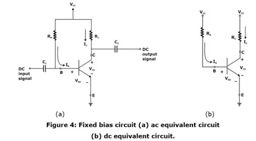
In figure 4(a), the base current is derived from supply voltage Vcc by resister RB. This type of biasing is called fixed bias as Vcc and RB are fixed quantities.

The operating point Q1 is chosen on load line for a particular Base current IB as shown in figure 4 (c)
By applying KVL in input loop,
IB = (VCC - VBE)/RB
Similarly, by applying KVL in output loop,
VCE = VCC - ICRC
IC = βIB + (1+β)ICO = βIB
Hence from above equ, Q-point (VCE, IC) is calculated for fixed IB.
Stability factor
∂IB/∂IC = 0
∴ Stability factor is given as
S= 1 + β
Disadvantage
If β = 100, the stability factor is 101 and the collector current is 101 times that ICO, reverse saturation current. Hence the stability factor for a fixed biased circuit is very high. So, it will be the least stable biasing arrangement. - Collector to base bias circuit
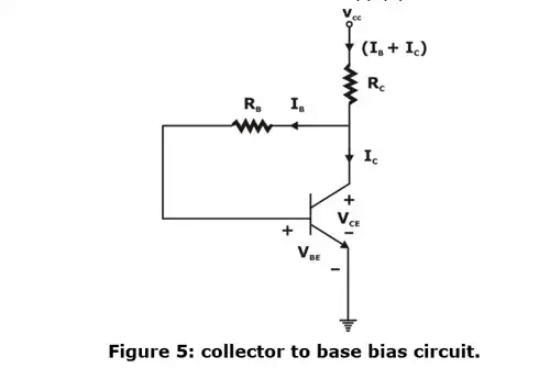
An improvement in bias stability is obtained if tapping for bias is taken from the collector terminal instead of from the collector supply point as shown in figure 5.
Applying KVL in input loop,
–VCC + (IB + IC) Rc + IBRB + VBE = 0
Now applying kVL in the output loop
–Vcc + Rc(IB + Ic) + VCE =0
⇒ VCE = VCC - RC(IB - IC)
With the help of above equ, operating point is calculated for given biasing circuit.
Stability factor
Advantage
The stability factor is smaller than (β + 1), hence an improvement in stability is obtained over a fixed bias circuit.
Disadvantage
(i) The stability factor depends upon RC. If Rc becomes smaller or zero, then the stability factor becomes very large and IC does not remain stable.
(ii) Resistance RB connected from collector to base causes negative feedback due to which voltage gain of the amplifier's circuit decreases. - Self-bias or Voltage-Divider bias

(i) If the collector resistance Rc is very small, for example, in a transformer coupled circuit, then there is no improvement in stabilization in collector to base bias circuit over the fixed bias circuit.
(ii) A circuit which can be used even if there is zero DC resistance in series with the collector terminal is self-biasing configuration of figure 6(a).
(iii) The current in resistance RE in emitter lead causes voltage drop which is in the direction of reverse biasing the emitter function.
(iv) Since this function must be forward biased, the base voltage is obtained from supply through R1, R2
(Note: If Rb = R1||R2 → 0, then base to ground voltage VBN is independent of ICO. Under these circumstances For best stability R1 and R2 must be kept as small as possible.)
(v) The given circuit in figure 6(a) can be simplified by using Thevenin’s theorem. Thevenin’s equivalent can be found between base and ground as shown in figure 6(b).
Now applying kVL in input loop
–V + IB Rb + VBE + (IB + IC) RE = 0
By using IC = βIB Again, applying kVL in output loop
-Vcc + IcRc + (IB + IC)RE + VcE = 0
VCE = VCC = IC(RC + RE) - IBRE
By using equation, operating point can be easily calculated.
Stability factor
Important point
(i) S varies between 1 for small Rb/RE and 1 + β for Rb/RE → infinity
(ii) A smaller value of Rb, better for stabilization.
(Note: even if Rb becomes zero, the value of S can’t be reduced below unity. Hence Ic always increases more than Ico.)
(iii) As Rb to reduced which Q-point to held fixed, the current drawn R1, R2 network from supply Vcc
(iv) Also, if Rc is increased while Rb is held constant then Vcc must be increased to operate at the same Q-point.
(v) In either case, a loss of power (decreased efficiency) to disadvantage accompanies the improvement in stability.
(vi) To avoid the loss of Ac (signal) gain because of feedback caused by Rc, this resistance is often passed by a large capacitance (> 10 μF), so that its reactance at frequencies under consideration is very small.
|
3 videos|33 docs|64 tests
|
FAQs on Circuits Analysis & Applications of Diodes, BJT, FET & MOSFET - 2 - Analog Circuits - Electronics and Communication Engineering (ECE)
| 1. What is the purpose of diodes in circuit analysis? |  |
| 2. How do BJT (Bipolar Junction Transistors) differ from FET (Field Effect Transistors)? |  |
| 3. What are the applications of MOSFETs (Metal-Oxide-Semiconductor Field-Effect Transistors)? |  |
| 4. How does a diode in forward bias operate? |  |
| 5. What is the difference between a diode and a zener diode? |  |

|
Explore Courses for Electronics and Communication Engineering (ECE) exam
|

|


 Again, applying kVL in output loop


