BJT as an Amplifier | Analog Circuits - Electronics and Communication Engineering (ECE) PDF Download
Introduction
- An amplifier is an electronic circuit designed by using an active device like bipolar junction transistor (BJT), field effect transistor (FET), that changes, usually increases the amplitude of the input signal (usually voltage or current).
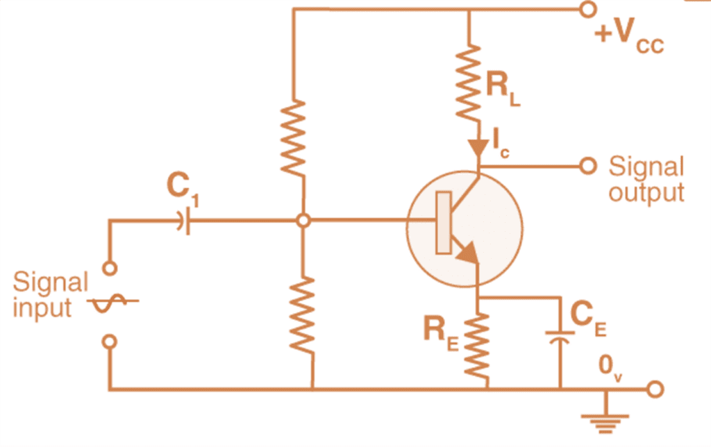 Transistor as an Amplifier
 - The relationship between the input and the output signals of an amplifier is expressed as a function of input frequency, commonly known as transfer function of amplifier.
Based upon the value of signal variation, amplifier can be classified in two types
(i) Small signal Amplifier
(ii) Large signal Amplifier
Small Signal Amplifier
- In the AC signal, signal variation and peak change value is maximum with respect to DC value.
- Small signal Amplifier is defined as an amplifier in which signal variation is much smaller than the DC value.
- From the characteristic curve of BJT, it can be seen that BJT is a nonlinear device. But in small signal amplifier BJT exhibits piece wise linearly or it simply behave as a linear element, that’s way small signal amplifier output signal will be distortion less. Small signal amplifier is used as voltage amplifier.
Large signal Amplifier
- In the ac amplifier in which signal variation is large or signal variation is comparable to dc value is known as large signal amplifier.
- Transistors behave as nonlinear element, in large signal amplifier due to which equal changes in base current do not produce proportional equal changes in collector current and output signal gets distorted.
- A large signal amplifier has large ac output current and voltage, and also it can supply greater ac output power to the load hence it is useful as power amplifier.
Small-Signal Variations
Consider the BJT circuit shown in figure 1. Various small signal parameters for the circuit are described below: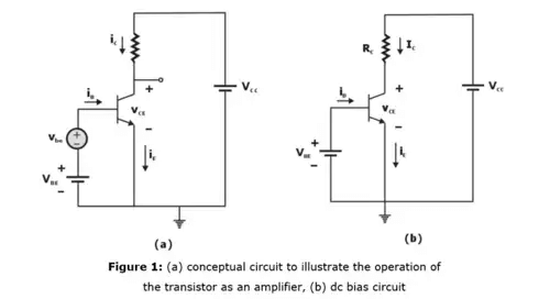
(i) Collector Current and the Transconductance
If a signal vbe is applied as shown in Figure 1, The total instantaneous base-emitter voltage vBE becomes
vBE = VBE + vbe
Instantaneous collector current becomes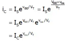
or, 
So, 
Thus, the instantaneous collector current is composed of the dc bias value IC and a signal component iC. So, signal current in the collector is:
ic = (IC/VT)vbe
It can be rewritten as
ic = gmVbe
where gm = IC/VT is called the transconductance.
(ii) Base Current and Input Resistance at the Base
To determine the resistance seen by Vbe, first evaluate the total base current iB using equation (V) as follows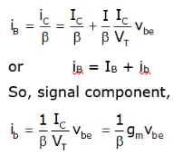
The small signal input resistance between base and emitter, looking into the base, is denoted by rπ and is defined as
or rx = βVT/IC
(iii) Emitter Current and the Input Resistance at the Emitter
Total Emitter current iE can be determined from equation (V) as:
or iE = IE + ie
So, we have the signal current,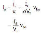
If we denote the small signal resistance between base and emitter, looking into the emitter, by re, it can be defined as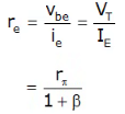
Small Signal Hybrid - Π Equivalent Circuit of BJT
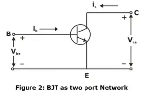
- A bipolar junction transistor can be treated as a two-port network as shown in figure 2. Small time-varying signals is superimposed at Q-point.
- Since the sinusoidal signals are small, the slope at Q-point is treated as constant, which has the units of conductance.
- The inverse of this conductance is the small-signal resistance defined as rπ. The small-signal input base current is related to the small-signal input voltage by:
vbe = ib rπ
where 1/rπ is equal to the slope of the iB – vBE curve. rπ can be found as given below,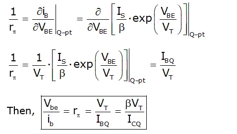
(Note: The resistance rπ is called diffusion resistance or base-emitter input resistance. rπ is a function of Q-point parameters.)
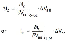
- While considering the output characteristics of bipolar transistor. Initially consider the case in which the output collector current is independent of the collector-emitter voltage, then the collector current is a function only of the base-emitter voltage. Then it can be written as,
Also,
Then,
- Then term IS exp (VBE/VT) evaluated at Q-point is just the quiescent collector current. The term ICQ/VT is conductance. Since this conductance relates a current in the collector to a voltage in the B-E circuit, the parameter is called transconductance and is written as:
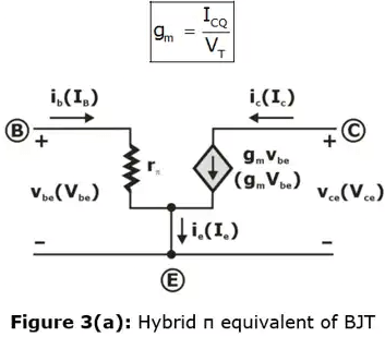
- Using these new parameters, a new simplified small-signal hybrid-π equivalent circuit can be developed for npn transistor, as shown in Figure 3(a).
The small-signal collector current is related to the small-signal base current as: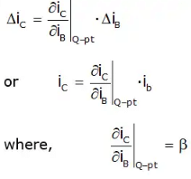
and is called an incremental or ac common-emitter current gain.
It can be written as,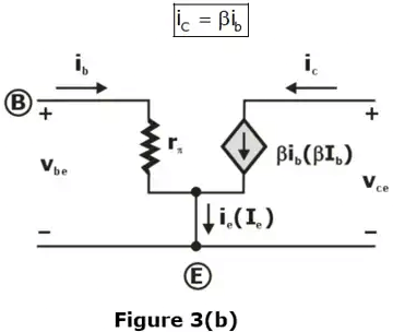
The small-signal equivalent circuit of bipolar transistor in Figure 3(b) uses this parameter.
Note: If rπ and gm is multiplied, then
Methodology to Analyse a BJT Amplifier
In linear amplifier circuits, superposition theorem is applicable, means the ac and dc analysis can be performed separately. The analysis of the BJT amplifier proceeds as follow:
- Step 1: Determine the dc operating point of the BJT and in particular the dc collector current Ic.
- Step 2: Calculate the values of the small signal model parameter,
gm = IC/VT, rπ = β/gm - Step 3: Eliminate the dc sources by replacing each dc current source with an open circuit.
- Step 4: Replace the BJT with one of its small signal equivalent circuit models. Although any one of the models can be used, one might be more convenient than the other for the particular circuit being analysed.
- Step 5: Analyse the resulting circuit to determine the required quantities (eg. Voltage gain, input resistance etc.).
Basic Transistor Amplifier Configurations
- As it is already discussed, the bipolar transistor is a three-terminal device, so three basic single-transistor amplifier configurations can be formed, depending on which of the three transistor terminals is used as signal ground.
- These three basic configurations are appropriately called common emitter, common collector (emitter-follower) and common base.
- The characteristics of these three types of amplifiers will be determined to show the conditions under which each amplifier is most useful.
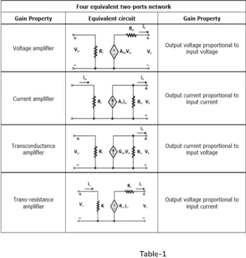
- Each of the three basic transistor amplifiers can be modelled as a two-port network in one of four configurations as shown Table 1.
Frequency Response of Common Emitter Amplifier
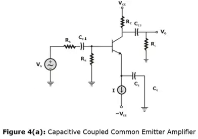
- In common emitter amplifier circuit of figure 4(a), it was assumed that the coupling capacitors Cc1 and Cc2 and the bypass capacitor CE were acting as perfect short circuits at the signal frequencies of interest, also there is neglected the internal capacitances of the BJT that is, Cπ and Cμ of the BJT high frequency model.
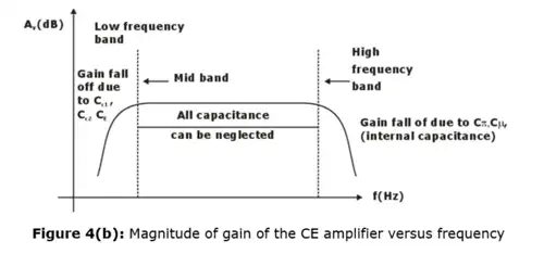
- It was assumed to be sufficiently small to act as open circuit at all signal frequency of interest. So, it is observed that the gain is almost constant over a wide frequency band, called the mid-band.
- Figure 4(b) shows that the gain fall off at signal frequencies below and above the mid-band.
- The gain fall-off in the low frequency band is due to the fact that even though CC1, CC2 and CE are large capacitance, as the signal frequency is reduced their impedance increase and they no longer behave as short circuit.
- On the other hand, the gain falloff in the high frequency band as result of Cgs and Cgd, which though very small, their impedance at sufficiently high frequency decrease, thus they can no longer be considered as open circuits.
(i) Cut-off Frequency
For a given circuit with equivalent resistance (Req) and equivalent capacitance (Ceq), the 3-dB cut-off frequency is given by:
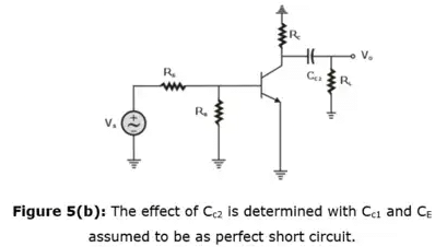
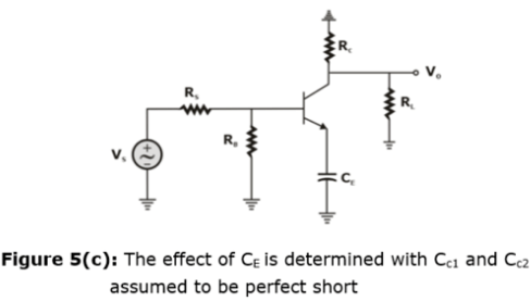
Thus, we calculate 3 dB frequencies due to CC1, CC2, CE as below.
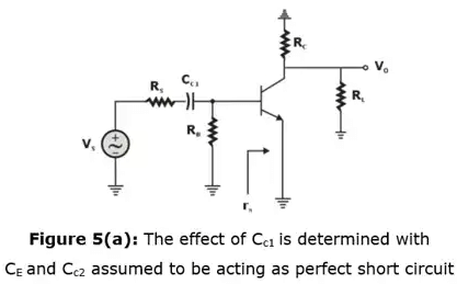
- The effect of CC1 is determined with CE and CC2 assumed to be acting as perfect short circuit as shown in figure 5(a). So,

- The 3dB frequency due to CC2 is given by

- The 3dB frequency due to CE is given by

FAQs on BJT Amplifier
Q.1. What is BJT Amplifier?
Ans: We have three types of BJT amplifiers based on the transistor configuration. Those are CB, CE, and CC amplifiers. We will use CB amplifiers as voltage amplifiers and current buffers. We will use CE amplifiers as power amplifiers. We will use CC amplifiers as current amplifiers and voltage buffers.
Q.2. What are the types of Amplifiers based on the frequency response?
Ans: Based on the requirement, we will do the amplification in some range of frequencies. Accordingly, we can classify the Amplifiers into these types. These are Direct Coupled (DC) amplifiers, Audio Frequency (AF) amplifiers, Radio Frequency (RF) amplifiers, Ultra High Frequency (UHF) and Microwave Frequency amplifiers.
Q.3. What is the need for biasing the transistor?
Ans: By using a transistor, we will amplify the AC signal at a small voltage level. For this, we must operate the BJT in a linear region or active region. To bring the transistor into this region, we should properly bias the transistor with the appropriate DC voltage.
Q.4. What is an emitter follower in BJT amplifier?
Ans: In the BJT amplifier which is configured in Common Collector (CC), the output voltage across the emitter terminal is the same as that of the voltage applied at the base terminal of BJT. Hence, it is called an emitter follower. The voltage gain of this circuit is equal to one.
Q.5. What is the current buffer in BJT amplifier?
Ans: In the BJT amplifier which is configured in Common Base (CB), the current through the collector terminal is the same as that of the current flowing through the emitter terminal of BJT. So, the current gain of the CB amplifier is equal to one. Hence, it is called a current buffer.
|
3 videos|66 docs|64 tests
|


