Bipolar Junction Transistors | Solid State Physics, Devices & Electronics PDF Download
Bipolar Junction Transistors
Transistor Construction
Transistor is a three-layer semiconductor device consisting of either two n- and one p-type layer of material or two p- and one n-type layers of material. The former is called npn transistor, while latter is called an pnp transistor. Both are shown in figure with proper biasing.
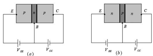
Figure: Types of transistors: (a) pnp (b) npn.
The emitter layer is heavily doped, the base lightly doped, and the collector only lightly doped. The outer layers have widths much greater than the sandwiched p- or n-type material. The ratio of the total width to that of the center layer is 150:1. The doping of the sandwiched layer is also considerably less than that of the outer layer (typically, 10:1 or less).This lower doping level decreases the conductivity (increases the resistance) of this material by limiting the number of “free” carriers.
The terminals have been indicated by the capital letters E for emitter, C for collector, and B for base. The term bipolar junction transistor (BJT) reflects the fact that holes and electrons participate in the injection process into the oppositely polarized material.
Transistor Operation
The basic operation of the transistor is described using pnp transistor as shown in figure (a). The operation of the npn transistor is exactly the same if the roles played by the electron and holes are interchanged. In figure the pnp transistor has been redrawn without the base-to-collector bias (similar to forward-biased diode). The depletion region has been reduced in width due to applied bias, resulting in a heavy flow of majority carriers from p- to the n-type material.
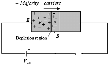
Figure : Forward-biased junction of a pnp transistor.
Let us now remove the base-to-emitter bias of the pnp transistor of figure (a) as shown in figure (similar to reverse-biased diode). Recall that the flow of majority carriers is zero, resulting in only a minority-carrier flow. Thus
“One p-n junction of a transistor is reversed biased, while the other is forward biased.”
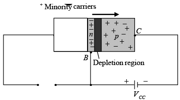
Figure : Reverse based junction of a pnp transistor.
In figure both biasing potentials have been applied to a pnp transistor, with the resulting majority and minority-carrier flow indicated. The widths of the depletion regions, indicating clearly which junction is forward-biased and which is reversed-biased. A large number of majority carriers will diffuse across the forward-biased p-n junction into the n-type material. Since n-type material is very thin and has low conductivity, a very small number of these carriers will take this path of high resistance to the base terminal. The larger number of these majority carriers will diffuse across the reverse biased junction into the p-type material connected to the collector terminal. Thus there has been an injection of minority carriers into the n-type base region material. Combining this with the fact that all the minority carriers in the depletion region will cross the reversed-biased junction of a diode accounts for the flow indicated in the figure.
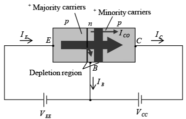 Figure : Majorit and minority carrier flow of a pnp transistor.
Applying Kirchhoff’s current law to the transistor of figure as if it were a single node, we obtain IE = IC + IB
The minority current component is called the leakage current and is given by the symbol ICO (collector current with emitter terminal open). The collector current, therefore is: 
Transistor Configurations
➤ Common-Base Configuration
The common-base configuration with pnp and npn transistors are shown in figure. The common-base terminology is derived from the fact that the base is common to both the input and output sides of the configurations.
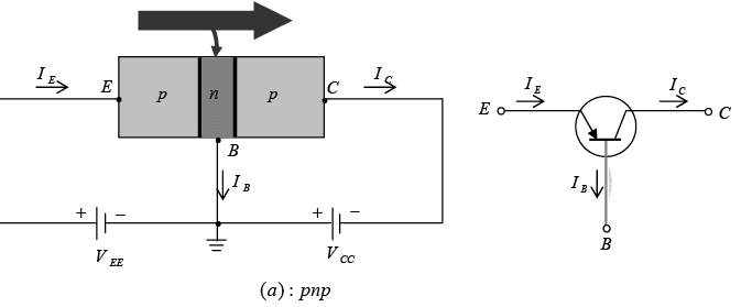
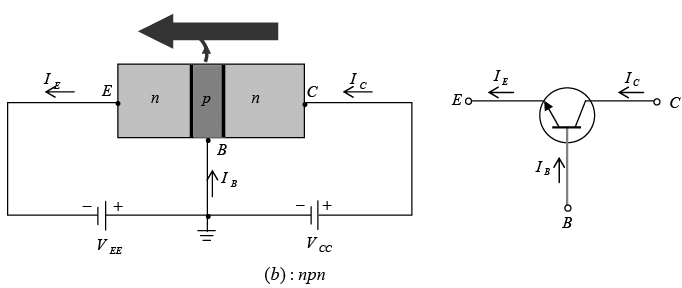
Figure : Notation and symbols used with the common base-configuration: (a) pnp transistor; (b) npn transistor.
To fully describe the behavior of a three terminal device such as common base amplifiers requires two set of characteristics- one for the driving point or input parameters and the other for the output side.
- Input Characteristics
The input set for the common base amplifiers as shown in figure will relate an input current (IE) to an input voltage (VBE) for various levels of output voltage (VCB).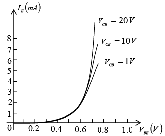 Figure : Input or driving point characteristics for a common-base silicon transistor.
 - Output Characteristics
The output set will relate an output current (IC) to an output voltage (VCB) for various levels of input current (IE). The output characteristics have three basic regions of interest: the active, cutoff, and saturation regions. The active region is the region normally employed for linear (undistorted) amplifiers.
In the active region the collector-base junction is reversed-biased, while the base-emitter junction is forward biased.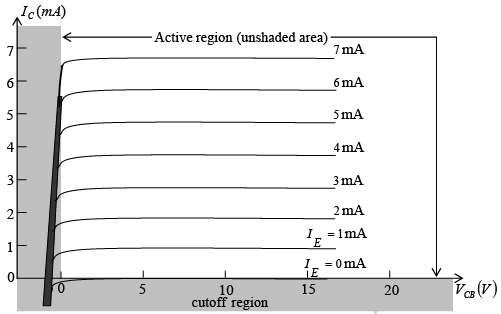 Figure : Output or collector characteristics for a common-base transistor amplifier. The circuit condition that exists when IE = 0 for common base configuration is shown in figure. Note that ICBO is temperature dependent and increases so rapidly with temperature.
In the output characteristics as the emitter current increases above zero, the collector current increases to a magnitude essentially equal to that of the emitter current as determined by the basic transistor current relations. Note also the almost negligible effect of VCB on the collector current for the active region. In the cutoff region the collector-base and base-emitter junctions are both reversed biased.
In the saturation region the collector-base and base-emitter junctions are both forward biased. - Alpha (α)
In the dc mode the levels of IC and IE due to majority carriers are related by a quantity called alpha and defined by the following equations:
αdc = IC/IE where IC and IE are the levels of current at the point of operation.
Thus
For ac situations where the point of operation moves on the characteristics curve, an ac alpha is defined by
The ac alpha is formally called the common-base, short-circuit, amplification factor.
The typical values of voltage amplification (V0/Vi)for the common-base configuration vary from 50 to 300. The current amplification (IC/IE) is always less than 1 for the common-base configuration.
➤ Common Emitter Configuration
The common-emitter configuration with pnp and npn transistors are shown in figure. The common-emitter terminology is derived from the fact that the emitter is common to both the input and output sides of the configurations.
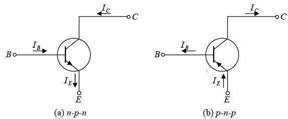 Figure : Notation and symbols used with the common-emitter configuration.
To fully describe the behavior of a three terminal device such as common emitter amplifier requires two set of characteristics- one for the input or base-emitter circuit and one for the output or collector-emitter circuit.
The output characteristics will relate an output current (IC) to an output voltage (VCE) for various levels of input current (IB). The input characteristics for the common emitter amplifiers will relate an input current (IB) to an input voltage (VBE) for various levels of output voltage (VCE).
In the active region the collector-base junction is reversed-biased, while the base-emitter junction is forward biased.
In the cutoff region the collector-base and base-emitter junctions are both reversed biased.
In the saturation region the collector-base and base-emitter junctions are both forward biased.
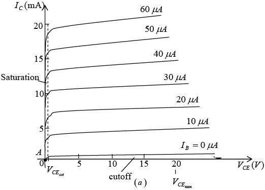
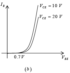
Figure : Characteristics of a silicon transistor in the common emitter configuration: (a) Collector characteristics; (b) base characteristics.
Since 
or 
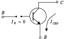 Figure : Circuit condition related to ICEO.
- Beta (β)
In the dc mode the levels of IC and IB are related by a quantity called beta and defined by the following equations: βdc = IC/IB where IC and IB are the levels of current at the point of operation. For ac situations where the point of operation moves on the characteristics curve, an ac beta is defined by The formal name for βac is common emitter forward-current amplification factor.
➤ Common-Collector Configuration
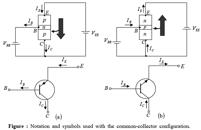
The third and final transistor configuration is the common–collector configuration, shown in figure with the proper current directions and voltage notation. The common collector configuration is used primarily for impedance-matching purposes since it has a high input impedance and low output impedance, opposite to that of the common-base and common-emitter configurations.
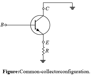
A common collector circuit configuration is provided in figure with the load resistor connected from emitter to ground. Note that the collector is tied to ground even though the transistor is connected in a manner similar to the common emitter configuration. For all practical purposes, the output characteristics of the CC configuration are same as for the CE configuration.
DC Biasing-BJTs
➤ Introduction
The analysis or design of a transistor amplifier requires knowledge of both the dc and ac response of the system. The improved output ac power level is the result of a transfer of energy from the applied dc supplies. The analysis or design of any electronic amplifier, therefore, has two components: the dc portion and the ac portion. Fortunately, the superposition theorem is applicable and the investigation of the dc conditions can be totally separated from the ac response. However, one must keep in mind that during the design stage the choice of parameters for the required dc levels will affect the ac response and vice-versa.
The dc level of operation of a transistor is controlled by a number of factors, including the range of possible operating points on the device characteristics. Each design will also determine the stability of the system, that is, how sensitive the system is to temperature variations.
Although a number of networks will be analyzed, there is an underlying similarly between the analysis of each configuration due to the recurring use of the following important basic relationships for a transistor:
VBE = 0.7V, IE = (β+1)IB≌IC and IC = βIB
➤ Operating Point
Since the operating point is a fixed point on the characteristics it is also called the quiescent point (abbreviated Q-point). By definition, quiescent means quiet, still, inactive. Figure shows a general output device characteristic with four operating points indicated. The biasing circuit can be designed to set the device operation at any of these points or others within the active region. The maximum ratings are indicated on the characteristics by a horizontal line for the maximum collector current  and a vertical line at the maximum collector-to-emitter voltage
  . The maximum power constraint is defined by the curve
  in the same figure. At the lower end of the scales are the cutoff regions, defined by IB ≤ 0 μA and the saturation region, defined by VCE ≤
 .
.
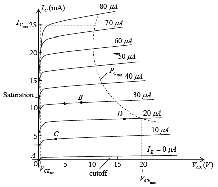
Figure : Various operating points within the limits of operation of a transistor.
If no bias were used, the device would initially be completely off, resulting in a Q-point at A-namely zero current through the device (and zero voltage across it). Since it is necessary to bias a device so that it can respond to the entire range of an input signal point A would not be suitable. For point B if a signal is applied to the circuit, the device will vary in current and voltage from operating point, allowing the device to react to both the positive and negative excursion of the input signal. If the input signal is properly chosen, the voltage and current of the device will vary but not enough to drive the device into cutoff or saturation. Point C would allow some positive and negative variation of the output signal but the peak-to-peak value would be limited by the proximity of VCE = 0V , IC = 0 mA . Operating at point C also raise some concern about the nonlinearities introduced by the fact that the spacing between IB curves is rapidly changing in this region.
In general, it is preferable to operate where the gain of the device is fairly constant (or linear) to ensure that the amplification over the entire swing of input signal is the same. Point D sets the device operating point near the maximum voltage and power level. The output voltage swing in the positive direction is thus limited if the maximum voltage is not to be exceeded. Point B is a region of more linear spacing and therefore, seems the best operating point in terms of linear gain and largest possible voltage and current swing. This is usually the desired condition for small-signal amplifiers but not the case necessarily for power amplifiers. In this discussion, we will be concentrating primarily on biasing the transistor for small-signal amplification operation.
Having selected and biased the BJT at a desired operating point, the effect of temperature must also be taken into account. Temperature causes the device parameters such as the transistor current gain (βac) and the transistor leakage current (ICEO) to change. Higher temperatures result in increased leakage currents in the device, thereby changing the operating condition set by the biasing network. The result is that the network design must also provide a degree of temperature stability so that temperature changes result in minimum changes in the operating point. This maintenance of the operating point can be specified by a stability factor, S, which indicates the degree of change in operating point due to a temperature variation. A highly stable circuit is desirable and the stability of a few basic bias circuits will be compared.
For the BJT to be biased in its linear or active operating region the following must be true:
- The base-emitter junction must be forward-biased (p-region voltage more positive) with a resulting forward-bias voltage of about 0.6 to 0.7 V.
- The base-collector junction must be reverse-biased (n-region more positive), with the reverse-bias voltage being any value within the maximum limits of the device.
Operation in the cutoff, saturation and linear regions of the BJT characteristic are provided as follows:
- Linear-region operation:
Base-emitter junction forward biased
Base-collector junction reversed biased - Cutoff-region operation:
Base-emitter junction reverse biased
Base-collector junction reversed biased - Saturation-region operation:
Base-emitter junction forward biased
Base-collector junction forward biased
Fixed-Bias Circuit
The fixed-bias circuit of figure provides a relatively straightforward and simple introduction to transistor dc bias analysis. Even though the network employs an npn transistor, the equations and calculations apply equally well to a pnp transistor configuration merely by changing all current directions and the voltage polarities.
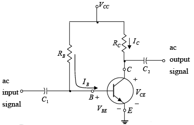 Figure : Fixed-bias circuit
For the dc analysis the network can be isolated from the indicated ac levels by replacing the capacitors with an open circuit equivalent. In addition, the dc supply VCC can be separated into two supplies (for analysis purposes only) as shown in figure to permit a separation of input and output circuits. It also reduces the linkage between the two to the base current IB.
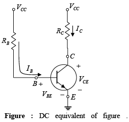
➤ Q-Point
- Forward Bias of Base-Emitter
Consider first the base-emitter circuit loop of figure shown. Writing Kirchhoff’s voltage equation in the clockwise direction for the loop, we obtain -VCC+IBRB+VBE = 0
Note the polarity of the voltage drop across RB as established by the indicated direction of IB. Solving the equation for the current IB will result in the following:
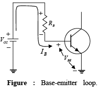 Since the supply voltage VCC and the base-emitter voltage VBE are constants, the selection of a base resistor, RB sets the level of base current for the operating point.
- Collector-Emitter Loop
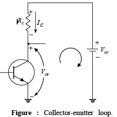
The collector-emitter section of the network appears in figure with the indicated direction of current IC and the resulting polarity across RC .
 The magnitude of the collector current is related directly to IB through
IC = βIB
It is interesting to note that since the base current is controlled by the level of RB and IC is related to IB by a constant β the magnitude of IC is not a function of the resistance RC . Change RC to any level and it will not affect the level of IB or IC as long as we remain in the active region of the device. However, as we shall see, the level of RC will determine the magnitude of VCE, which is an important parameter.
Applying Kirchhoff’s voltage law in the clockwise direction around the indicated closed loop of figure will result in the following:
−VCC+ICRC + VCE = 0 ⇒ VCE=VCC − ICRC
As a brief review of single and double subscript notation recall that VCE =VC-VE
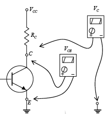 Figure : Measuring VCE and VC .
where VCE is the voltage from collector to emitter and VC and VE are the voltages from collector and emitter to ground respectively. But in this case since VE=0V, we have VCE=VC.
In addition, since VBE =VB− VE and VE = 0V then VBE =VB.
Keep in mind that voltage levels such as VCE are determined by placing the positive lead of the voltmeter at the collector terminal with the negative lead at the emitter terminal as shown in figure. VC is the voltage from collector to ground and is measured as shown in the same figure. In this case the two readings are identical, but in the networks to follow the two can be quite different.
➤ Transistor Saturation
The term saturation is applied to any system where levels have reached their maximum values. For a transistor operating in the saturation region the current is a maximum value for the particular design. Change the design and the corresponding saturation level may rise or drop.
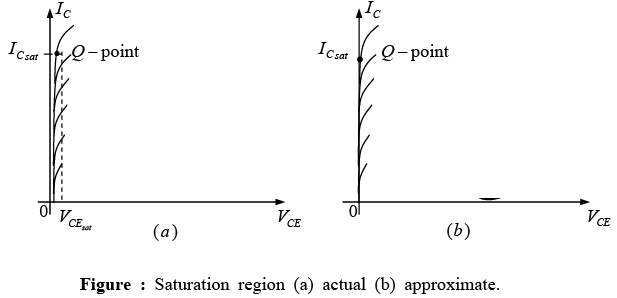
Saturation conditions are normally avoided because the base-collector junction is no longer reverse-biased and the output amplified signal will be distorted. An operating point in the saturation region is depicted in figure. Note that it is in a region where the characteristic curves join and the collector-to-emitter voltage is at or below . In
. In
addition, the collector current is relatively high on the characteristics.
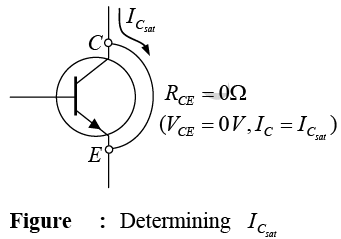
If we approximate the curves of figure (a) by those appearing in figure (b), a quick direct method for determining the saturation level becomes apparent. In figure (b) the current is relatively high and the voltage VCE is assumed to be zero volts. Applying Ohm’s law the resistance between collector and emitter terminals can be determined as follows:

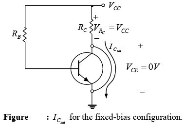
For saturation current set VCE = 0V and find  . For the fixed-bias configuration of figure the short circuit has been applied, causing the voltage across RC to be the applied voltage VCC. The resulting saturation current for the fixed-bias configuration is
➤ Load-Line Analysis
We will now investigate how the network parameters define the possible range of Q-points and how the actual Q-point is determined.
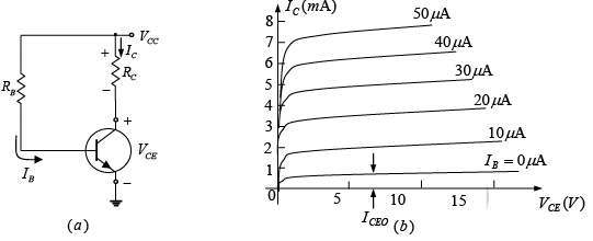 Figure : Load-line analysis (a) the network (b) the device characteristics.
The network of figure (a) establishes an output equation that relates the variables IC and VCE in the following manner: VCE =VCC− IC RC
The output characteristics of the transistor also relate the same two variables IC and VCE in figure (b).
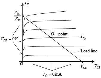 Figure : Fixed-bias load.
We must now superimpose the straight line defined by equation VCE =VCC− IC RC on the characteristics. If we choose IC to be 0 mA , we are specifying the horizontal axis as the line on which one point is located. By substituting IC = 0 mA , we find that  defining one point for the straight line as shown in figure.
If we now choose VCE to be 0 V , which establishes the vertical axis as the line on which the second point will be defined, we find that IC is determined by the following equation:
By joining the two points defined by equation 
the straight line established by equation VCE =VCC − ICRC can be drawn. The resulting line on the graph of figure is called the load line since it is defined by the load resistor RC. By solving for the resulting level of IB the actual Q-point can be established. If the level of IB is changed by varying the value of RB the Q-point moves up or down the load line as shown in figure.
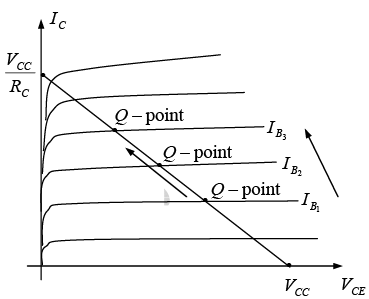 Figure : Movement of Q-point with increasing levels of IB.
NOTE: For Fixed RB if temperature of the device increases the Q-point will moves towards the saturation region as shown in figure. Since IC = βIB+ICEO with increase in temperature reverse current ICEO = (β+) ICBO increases.
If VCC is held fixed and RC changed, the load line will shift as shown in figure. If IB is held fixed, the Q-point will move as shown in the same figure.
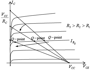
Figure : Effect of increasing levels of RC on the load line and Q-point.
If RC is fixed and VCC varied, the load line shifts as shown in figure.
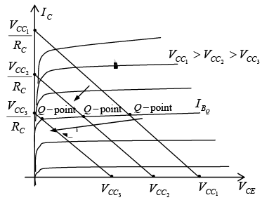 Figure : Effect of lower values of VCC on the load line and Q-point.
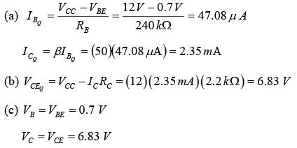
Example: Determine the following for the fixed-bias configuration of figure shown below.
(a) 
(b) 
(c) VB and VC
(d) VBC
(e) Saturation level.
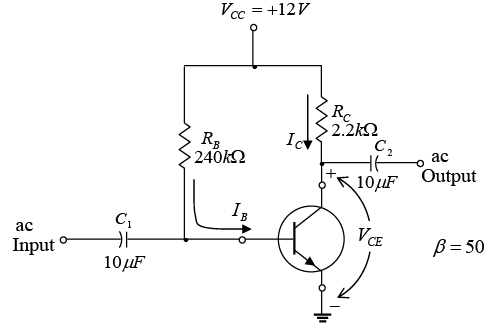
(d) Using double-subscript notation yields
VBC = VB - VC = 0.7V - 6.83V = -6.13V
With the negative sign revealing that the junction is reversed-biased, as it should be for linear amplification.
(e)which is far from the saturation level and about one-half the maximum value for the design.
Emitter-Stabilized Bias Circuit
The dc bias network of figure contains an emitter resistor to improve the stability level over that of the fixed-bias configuration.
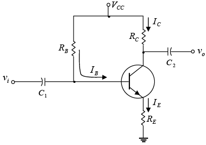
Figure : BJT circuit with emitter resistor.
➤ Q-Point
The analysis will be performed by first examining the base-emitter loop and then using the results to investigate the collector-emitter loop.
- Base–Emitter Loop
The base-emitter loop of the network can be redrawn as shown in figure. Writing Kirchhoff’s voltage law around the indicated loop in the clockwise direction will result in the following equation:
-VCC+IBRB+VBE+IERE= 0
VCC − IBRB− VBE − (β + 1) IBRE = 0 ∵ IE = (β+ 1)IB
Grouping terms will then provide the following: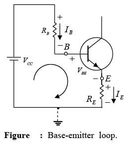

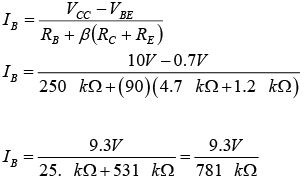
Note that the only difference between this equation for IB and that obtained for the fixed-bias configuration is the term (β + 1) RE.
There is an interesting result that can be derived from equation if the equation is used to sketch a series network that would result in the same equation. Such is the case for the network of figure. Solving for the current IB will result in the same equation obtained above. Note that aside from the base-to-emitter voltage VBE the resistor RE is reflected back to the input base circuit by a factor (β + 1). In other words, the emitter resistor, which is part of the collector–emitter loop, “appears as” (β + 1) RE in the base-emitter loop. Since β is typically 50 or more, the emitter resistor appears to be a great deal larger in the base circuit.
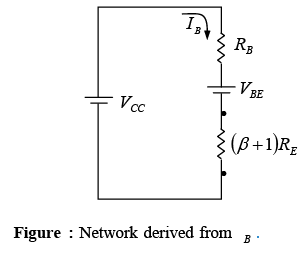
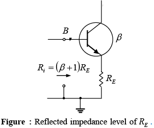 In general, therefore, for the configuration of figure, Ri = (β+1)RE
This equation is one that will prove useful in the analysis to follow. In fact, it provides a fairly easy way to remember equation Using Ohm’s law, we know that the current through a system is the voltage divided by the resistance of the circuit. For the base-emitter circuit the net voltage is VCC −VBE. The resistance levels are RB plus RE reflected by (β + 1) .
 - Collector–Emitter Loop
The collector-emitter loop is redrawn in figure. Writing Kirchhoff’s voltage law for the indicated loop in the clockwise direction will result in IERE + VCE + ICRC - VCC = 0
Substituting IC ≈ IE and grouping terms gives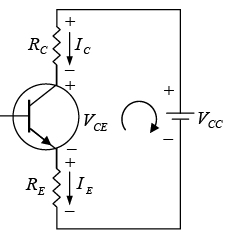 Figure : Collector-emitter loop.
VCE =VCC− IC ( RC + RE)
The single-subscript voltage VE is the voltage from emitter to ground and is determined by VE =IERE
while the voltage from collector to ground can be determined from VCE =VC− VE or VC =VCE+ VE and VC =VCC − ICRC
The voltage at the base with respect to ground can be determined from VB =VCC− IB RB or VB =VBE + VE - Saturation Level
The collector saturation level or maximum collector current for an emitter-bias design can be determined using the same approach applied to the fixed-bias configuration:
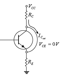 Figure : Determining
  for the emitter-stabilized bias circuit.
The addition of the emitter resistor reduces the collector saturation level below that obtained with a fixed-bias configuration using the same collector resistor. - Load-Line Analysis
The load-line analysis of the emitter-bias network is only slightly different from that encountered for the fixed-bias configuration. The level of IB as determined by equation defines the level of IB on the characteristics of figure (denoted
  ).
).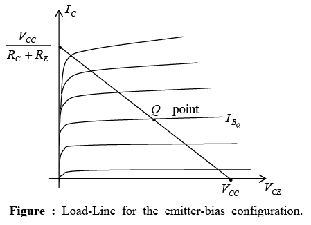 The collector-emitter loop equation that defines the load line is the following:
as obtained for the fixed-bias configuration. Choosing VCE = 0V gives as shown in figure. Different levels of
  will, of course, move the Q-point up or down the load line.
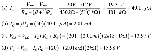
Example: For the emitter bias network of figure shown below, determine:
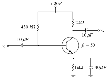
(a) IB
(b) IC
(c) VCE
(d) VC
(e) VE
(f) VB
(g) VBC
(h) 
which is about twice the level of.
Voltage-Divider Bias
In the previous bias configurations the bias current  and voltage
  were a function of the current gain (β) of the transistor. However, since β is temperature sensitive, specially for silicon transistors, and the actual value of beta is usually not well defined, it would be desirable to develop a bias circuit that is less dependent, or in fact, independent of the transistor beta. The voltage-divider bias configuration of figure is such a network. If analyzed on an exact basis the sensitivity to changes in beta is quite small.
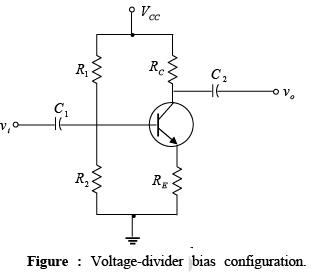
➤ Q-point
The input side of the network can be redrawn as shown in figure for the dc analysis. The Thevenin equivalent network for the network to the left of the base terminal can then be found in the following manner. 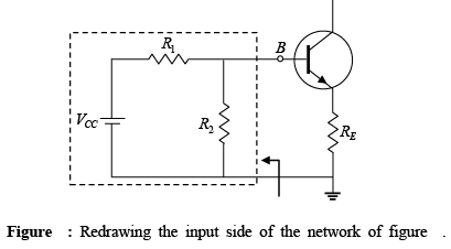
- Thevenin’s Resistance (RTh) : The voltage source is replaced by a short-circuit equivalent as shown in figure .

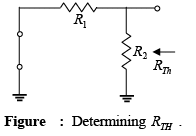
- Thevenin’s Voltage ( ETh) : The voltage source VCC is returned to the network and the open-circuit Thevenin voltage of figure determined as follows:
Applying the voltage-divider rule:
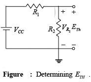 The Thevenin network is then redrawn as shown in figure 3.39 and
  can be determined by first applying Kirchhoff’s voltage law in the clockwise direction for the loop indicated: -ETh + IBRTh + VBE + IERE = 0
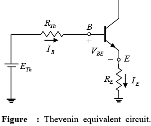 Once IB is known the remaining quantities of the network can be found in the same manner as developed for the emitter-bias configuration. That is VCE = VCC-IC(RC+RE).
The remaining equations for VE , VC and VB are also the same as obtained for the emitter-bias configuration.
➤ Transistor Saturation
The output collector-emitter circuit for the voltage-divider configuration has the same appearance as the emitter-biased circuit. The resulting equation for the saturation current (when VCE is set to zero volts on the schematic) is therefore the same as obtained for the emitter-biased configuration. That is, 
➤ Load-Line Analysis
The similarities with the output circuit of the emitter-biased configuration result in the same intersections for the load line of the voltage-divider configuration. The load line will therefore have the same appearance as that of figure, with  and
and 
The level of IB is of course determined by a different equation for the voltage-divider bias and the emitter-bias configurations.
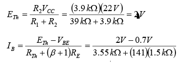
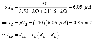
Example: Determine the dc bias voltage VCE and the current IC for the voltage-divider configuration of figure shown below.
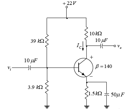
⇒ VCE= 22 − ( 0.85mA) (10k Ω + 1.5k Ω ) = 12.22 V
DC Bias with Voltage Feedback
An improved level of stability can also be obtained by introducing a feedback path from collector to base as shown in figure.
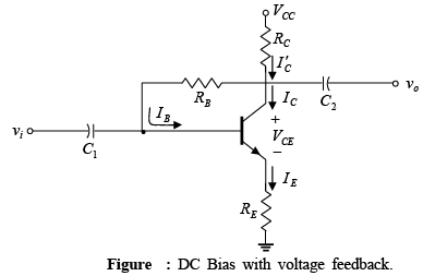
➤ Q-point (Base-Emitter Loop)
Figure shows the base-emitter loop for the voltage feedback configuration. Writing Kirchhoff’s voltage law around the indicated loop in the clockwise direction will result in
−VCC+IC′ RC + IBRB + VBE + IERE = 0
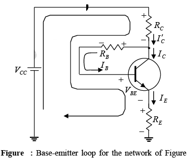
It is important to note that the current through RC is not IC but IC′ (where IC′ = IC+IB ≈ IC). Thus
In general, therefore, the feedback path results in a reflection of the resistance RC back to the input circuit, much like the reflection of RE.
In general, the equation for IB had the following format:  with the absence of R′ for the fixed-bias configuration, R′ = RE for the emitter-bias setup (with (β + 1)≅ β ), and R′ = RC+RE for the collector-feedback arrangement. The voltage V ′ is the difference between two voltage levels.
 ∵ IC = βIB
➤ Collector-Emitter Loop
The collector-emitter loop for the network is provided in figure. Applying Kirchhoff’s voltage law around the indicated loop in the clockwise direction will result in −VCC+IC′ RC + VCE + IERE = 0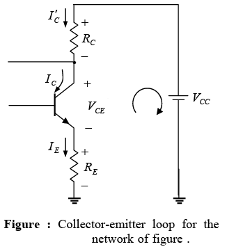
−VCC+IC (RC + RE) + VCE = 0
∵ I'C = IC and IE = IC
⇒ VCE = VCC − IC ( RC + RE)
which is exactly as obtained for the emitter-bias and voltage-divider bias configurations.
➤ Saturation Conditions
Using the approximation IC′ = IC the equation for the saturation current is the same as obtained for the voltage-divider and emitter-bias configurations. That is,
➤ Load-Line Analysis
Continuing with the approximation IC′ = IC will result in the same load line defined for the voltage-divider and emitter-biased configurations. The level of  will be defined by
the chosen bias configuration.
Example: Determine the quiescent levels of  and
and  for the network of figure shown below.
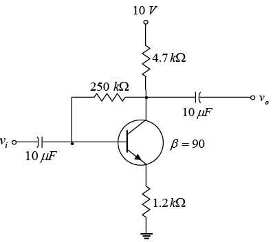
IB = 11.91 μA
|
91 videos|21 docs|25 tests
|
FAQs on Bipolar Junction Transistors - Solid State Physics, Devices & Electronics
| 1. What is a bipolar junction transistor? |  |
| 2. How does a bipolar junction transistor work? |  |
| 3. What are the different types of bipolar junction transistors? |  |
| 4. What are the applications of bipolar junction transistors? |  |
| 5. What are the advantages of bipolar junction transistors? |  |

