Digital Electronics | Solid State Physics, Devices & Electronics PDF Download
Digital Electronics
Number System
➤ Decimal Numbers
Decimal number system uses ten digits, that is, a system with base of ten. Each of the ten decimal digits, 0 through 9, represents the certain quantity. The position of each of the digits in the decimal number indicates the magnitudes of the quantity represented and can be assigned a “weight”.
The value of a decimal number is the sum of the digits times their respective column weights.
Example : 23 = 2 × 10 + 3 × 1 = 20 + 3 = 23
The digit 2 has a weight of 10, as indicated by its position, and the digit 3 has a weight of 1, as indicated by its position.
Example : 568 = 5×100 + 6 ×10 + 8 ×1 = 500 + 60 + 8 = 568
The digit 5 has weight of 100, the digit 6 has a weight of 10, and the digit 8 has a weight of 1.
➤ Binary Numbers
The binary system with its two digits is a base-two system. The two binary digits (bits) are 1 and 0. The position of the 1 or 0 in a binary number indicates its “weight”. The weight of each successively higher position (to the left) in a binary number is an increasing power of two.
Highest decimal number with n bits = 2n − 1
For instance, with two bits we can count from 0 through 3 (22 −1 = 3).
- Binary-to-Decimal Conversion
The value of a given binary number in terms of its decimal equivalent can be determined by adding the products of each bit and its weight. The right-most bit is the least significant bit (LSB) in a binary number and has a weight of 20 =1. The weights increase by a power of two for each bit from right to left.
Example : Convert (1101101) to decimal number.

1×64+1× 32 + 0×16 +1×8 +1× 4 + 0× 2 +1×1 = 64 + 32 + 0 + 8 + 4 + 0 +1 = 10910
The binary numbers we have seen so far have been whole numbers. Fractional number can also be represented in binary by placing bits to the right of the binary point, just as fractional decimal digits are placed to the right of the decimal point.
The column weights of a binary number are
This indicates that all the bits to the left of the binary point have weights that are positive powers of two and to the right of the binary point have weights that are negative powers of two.
Example : Convert (0.1011) to decimal number.
1×0.5+ 0 × 0.25 + 1× 0.125 + 1× 0.0625 = 0.5 + 0 + 0.125 + 0.0625 = 0.687510.
Example : Convert (11101.011) to decimal number.
(16 + 8+ 4 + 1) . ( 0.25 + 0.125) = 29.37510
- Binary addition and subtraction
There are four basic rules for adding binary digits:
There are four basic rules for subtracting binary digits:
- 1's and 2's compliments
The 1's compliment of a binary number is found by simply changing all 1's to 0's and all 0's to 1's. The 2's compliment of a binary number is found by adding 1 to the 1's compliment.
Example: 
- Decimal-to-Binary Conversion
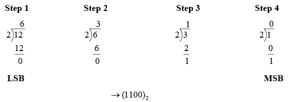
In a repeated division-by-2 process we begin by dividing decimal number by 2 and then dividing each resulting quotient by 2 until there is a 0 quotient. The remainders generated by each division form the binary number. The first remainder to be produced is the least significant bit (LSB) in the binary number.
Example: Convert decimal number 12 to binary number.
- Converting Decimal Fraction to Binary
In a repeated multiplication-by-2 process we begin by multiplying decimal number by 2 and then multiplying each resulting fractional part by 2 until the fractional product is zero. The carry generated by each multiplication form the binary number. The first carry produced is the most significant bit (MSB) in the binary number.
Example: Convert decimal number 0.3125 to binary number.
Step 1 → 0.3125 × 2= 0.625 → carry = 0 ( MSB)
Step 2 → 0.625 × 2= 1.25 → carry = 1
Step 3 → 0.25 × 2= 0.50 → carry = 0
Step 4 → 0.50 × 2= 1.00 → carry = 1 ( LSB) → (0.0101)2
➤ Octal Numbers
The octal number system is composed of eight digits, which are 0, 1, 2, 3, 4, 5, 6, 7 .
Counting in octal is the same as counting in decimal, except any number with an 8 or a 9 is omitted. It is a system with base eight.
- Octal-to-Decimal Conversion
Since the octal number system has a base of eight, each successive digit position is an increasing power of eight, beginning in the right-most column with 80. The evaluation of an octal number in terms of its decimal equivalent is accomplished by multiplying each digit by its weight and summing the products.
Example : Convert (2374)8 to decimal number.
2×512+ 3× 64 + 7 ×8 + 4×1 = 127610The octal numbers we have seen so far have been whole numbers. Fractional octal numbers are represented by digits to the right of the octal point.
The column weights of an octal number are
8n...83828180.8−18−2...8−n
This indicates that all the digits to the left of the octal point have weights that are positive powers of eight and to the right of the octal point have weights that are negative powers of eight.
Example : Convert (0.325)8 to decimal number.
3 ×0.125+ 2 × 0.015625 + 5 × 0.001953 = 0.41601510
- Decimal-to-Octal Conversion
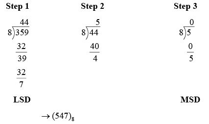
In a repeated division-by-8 process we begin by dividing decimal number by 8 and then dividing each resulting quotient by 8 until there is a 0 quotient. The remainders generated by each division form the octal number. The first remainder to be produced is the least significant digit (LSD) in the octal number.
Example: Convert decimal number 359 to octal number.
- Octal-to-Binary Conversion
The primary application of octal numbers in is in the representation of binary numbers. Since it takes only one octal digit to represent three bits, octal numbers are much easier to “read” than binary numbers.
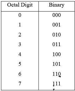
Because all three-bit binary numbers are required to represent the eight octal digits, it is very easy to convert from octal to binary and from binary to octal. The octal number system is often used in digital systems, especially for input/output applications. Each octal digit is represented by three bits as indicated:
To convert an octal number to a binary number, simply replace each octal digit by the appropriate three bits. This is illustrated in the following example.
Example: Convert each of the following octal numbers to binary
(a) 138 (b) 258 (c) 478 (d) 1708 (e) 7528 (f) 52768 (g) 37.128
- Binary-to-octal Conversion
Conversion of a binary number to an octal number is also a straightforward process. Beginning at the binary point, simply break the binary number into groups of three bits and convert each group into the appropriate octal digit.
Example: Represent each of the following binary numbers by its octal equivalent:
(a) 1101012 (b) 1011110012 (c) 10111001102 (d) 1001101.10112
➤ Hexadecimal Numbers
The hexadecimal system has a base of sixteen; that is, it is composed of 16 digits and characters. Many digital systems process binary data in groups that are multiples of four bits, making the hexadecimal number very convenient because each hexadecimal digit represents a four-bit binary number (as listed in Table 2-2).
Ten digits and six alphabetic characters make up this number system. A subscript 16 indicates a hexadecimal number. 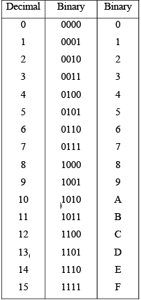
- Binary-to-Hexadecimal Conversion
Converting a binary number to hexadecimal is a straightforward procedure. Simply break the binary number into four-bit groups starting at the binary point, and replace each group with the equivalent hexadecimal symbol.
Example: (a) 11001010010101112 (b) 1111110001011010012 (c) 1110011000.1112
➤ Hexadecimal-to-Binary Conversion
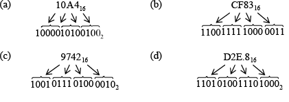
To convert from a hexadecimal number to a binary number, reverse the process and replace each hexadecimal symbol with the appropriate four bits.
Example: Determine the binary numbers for the following hexadecimal numbers:
(a) 10A416 (b) CF8316 (c) 974216 (d) D2E.816
➤ Hexadecimal-to-Decimal Conversion
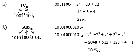
One way to evaluate a hexadecimal number in terms of its decimal equivalent is first convert from binary decimal. The following example illustrates this procedure.
Example: Convert the following hexadecimal numbers to decimal.
(a) 1C16 (b) A8516
Another way to convert a hexadecimal number to its decimal equivalent is by multiplying each hexadecimal digit by its weight and then taking the sum of these products. The weights of a hexadecimal number are increasing powers of 16 (from right to left). For a four-digit hexadecimal number the weights are
The following example shows this conversion method.
Example: Convert (a) E516 and (b) B2F816 to decimal.
E516 = E×16 + 5 ×1 = 14 ×16 +5 ×1 = 224 +5 = 22910
B2F816 = B× 4096 + 2 × 256 + F ×16 + 8 ×1
= 11× 4096 + 2 × 256 + 15 ×16 + 8 ×1
= 45056 + 512 + 240 + 8=4581610
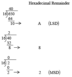
Decimal to Hexadecimal number formed by the reminders of each division. This is similar to the repeated division-by-2 for decimal-to-binary conversion and repeated division-by-8 for decimal-to-octal conversion.
Example: Convert 65010 to hexadecimal by repeated division by 1610.

Therefore, 65010 = 28A16.
Logic Gates
➤ The Inverter
The inverter (NOT circuit) performs a basic logic function called inversion or complementation. The purpose of the inverter is to change one logic level to opposite level. In terms of bits, it changes a 1 to a 0 and a 0 to a 1.
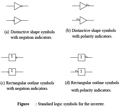
Standard logic symbols for the inverter are shown in figure. Figure (a) and (b) show the distinctive shape symbols and parts (c) and (d) show the rectangular outline symbols. In this text, distinctive shape symbols used; however, the rectangular outline symbols are commonly found in industry publications, and you should become familiar with them as well.
- The Negation and Polarity Indicators
The negation indicator is a “bubble” (º) appearing on the input or output logic element, as shown in figure (a) and (c). When appearing on the input, bubble means that an external 0 produces an internal 1. When appearing on output, the bubble means that an internal 1 produces an external 0. Typically inputs are on the left of a logic symbol and outputs are on the right.
The polarity indicator is a “triangle” appearing on the input or output of a logic element, as shown in figure (b) and (d). When appearing on input, it means that an external LOW level produces an internal HIGH. When appearing on the output, it means that an internal HIGH produces an external LOW level. Either indicator (bubble or triangular) can be used on both distinctive shape symbols and rectangular outlines as indicated. The placement of the negation or polarity indicator does not imply a change in the way an inerter operates.
Because positive logic (HIGH = 1, LOW = 0) is used in this text, both indicators are equivalent and can be interchanged. However, we will use primarily the negation indicator (bubble) throughout this text to represent an inversion.
The placement of the bubble on the input or output of a logic element is determined by the active state of the input signal (pulse or level). The active state is the state (1 or 0) when the signal is considered to be present on the input. When the active state of the input is a 0, the bubble is placed on the input. When the active output state is a 0, the bubble is placed on the output. - Inverter Operation
When a HIGH level is applied to an inverter input, a LOW level will appear on its output. When a LOW level is applied to its input, a HIGH will appear on its output. This operation is summarized in Table given below, which shows the output for each possible input in terms of levels and bits. These tables are called truth tables.
TABLE: Inverter Truth Tables
- Pulsed Operation
Figure shows the output of an inverter for a pulse input where t1 and t2 indicate the corresponding points on the input and output pulse waveforms. Note that when the input is LOW, the output is HIGH, and when the input is HIGH, the output is LOW, thereby producing an inverted output pulse.
Example: A pulse waveform is applied to an inverter as shown in figure. Determine the output waveform corresponding to the input.
The output waveform is exactly opposite to the input (inverted) at each point.
➤ The AND Gate
The AND gate performs logical multiplication, more commonly known as the AND function. The AND gate is composed of two or more inputs and a single output, as indicated by the standard logic symbols shown in figure. Inputs are on the left and the output is on the right in each symbol. Gates with two and four inputs are shown; however, an AND gate can have any number of inputs greater than one.
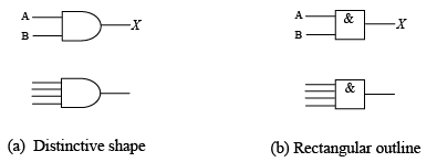
Figure : Standard logic symbols for the AND gate showing two and four inputs.
- Logical Operation of the AND Gate
The operation of the AND gate is such that the output is HIGH only when all of the inputs are HIGH. When any of the inputs are LOW, the output is LOW.
The truth table can be expanded for any number of inputs.
Table: Truth table for a two-input AND gate.
- Pulsed Operation
 Figure : Example of pulsed AND gate operation.
➤ The OR Gate
The OR gate performs logical addition, more commonly known as the OR function. An OR gate has two or more inputs and one output, as indicated by standard logic symbols shown in figure where OR gates with two and four inputs are illustrated.  Figure : Standard logic symbols for the OR gate showing two and four inputs.
- Logical Operation of the OR Gate
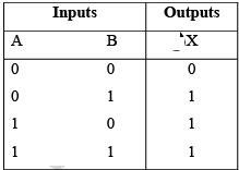
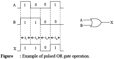
The operation of the OR gate is such that a HIGH on the output is produced when any of the inputs are HIGH. The output is LOW only when all of the inputs are LOW.
Table: Truth table for a two-input OR gate.
- Pulsed Operation

➤ The NAND Gate
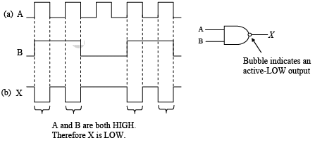
The term NAND is a contraction of NOT-AND and implies an AND function with a complemented (inverted) output. A standard logic symbol for a two-input NAND gate and its equivalency to an AND gate followed by an inverter are shown in figure (a). A rectangular outline representation is shown in part (b).  Figure : Standard NAND gate logic symbols.
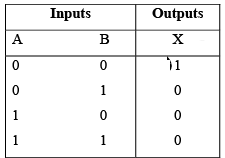
The NAND gate is very popular logic function because it is a “universal” function; that is, it can be used to construct an AND gate, an OR gate, an inverter, or any combination of these functions. Truth table for a two-input NAND gate.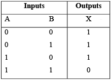
- Pulsed Operation

➤ The NOR Gate
The term NOR is a contraction of NOT-OR and implies an OR function with inverted output. A standard logic symbol for a two input NOR gate and equivalent OR gate followed by an inverter are shown in figure (a). A rectangular outline symbol is shown in part (b). Figure : Standard NOR gate logic symbols.
The NOR gate, like the NAND, is a very useful logic gate because of universal property.
- Truth table for a two-input gate

Figure : Standard NOR gate logic symbols. - Pulsed Operation:

➤ OR Gate (Positive Logic and Negative Logic) OR Gate (Positive logic)
The truth table can be verified for the circuit shown in figure. In positive logic V (1) means HIGH voltage and V(0) means LOW voltage. When both inputs have LOW voltage output will be V(0) i.e. LOW voltage. When any of the input is HIGH, the output will be V (1) i.e. HIGH as explained below.
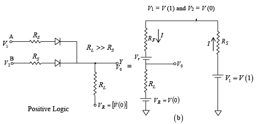 Figure : (a) Positive logic OR Gate (b) Equivalent circuit for analysis.
Apply K.V.L. 
V0 =IRL+ V (0) = V (1) − V (0)] + V(0) ⇒ V0 = V (1) .
Similarly when any of the input is 1 output is V (1). When both inputs are 0 output is V(0).
- OR Gate (Negative logic)
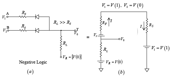
The truth table can be verified for the circuit shown in figure. In negative logic V (1) means LOW voltage and V(0) means HIGH voltage. When both inputs have HIGH voltage [V(0)] output will be V(0) . When any of the input is LOW [V (1)], the output will be V (1) i.e. LOW as explained below. Apply K.V.L.
∵ RL >> RF + RS and Vγ is very small.
V0 = V− IRL = V(0) − [V(0) − V(1)] ⇒ V0=V (1)
➤ AND Gate (Positive Logic and Negative Logic)
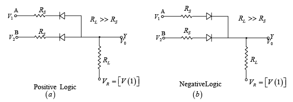
Figure : (a) Positive logic AND Gate (b) Negative logic AND Gate.
We can easily verify truth table of AND gate by drawing equivalent circuit in each case.
Logic Expressions
➤ NOT
The operation of an inverter (NOT circuit) can be expressed with symbols as follows: If the input variable is called A and the output variable is called X then X =  This expression states that the output is the complement of the input, so that if A = 0 , then X = 1 and if A = 1 , then X = 0 .
 Figure : The inverter complements an input variable.
➤ AND
The operation of a two-point AND gate can be expressed in equation form as follows: If one input variable is A , the other input variable is B , and the output variable is X , then the Boolean expression for this basic gate function is X = AB . Figure shows the gate with the input and output variables indicated.  Figure : Boolean expression for AND functions.
➤ OR
The operation of a two-input OR gate can be expressed in equation form as follows: If one input is A , the other input is B , and the output is X , then the Boolean expression is X = A+B . Figure shows the gate logic symbol, with input and output variables labeled. Figure : Boolean expressions for OR functions.
➤ NAND
The Boolean expression for a two-input NAND gate is X =  . This expression says that the two input variables, A and B , are first ANDed and then complemented, as indicated by the bar over the AND expression.
➤ NOR
Finally, the expression for a two input NOR gate can be written as X =  . This equation says that the two input variables are first O Red and then complemented, as indicated by the bar over the OR expression.
Rules for Boolean algebra
Basic rules that are useful in manipulating and simplifying Boolean algebra expressions are given below: 
➤ Demorgan’s Theorems
These theorems are illustrated by the gate equivalencies and truth tables in figure. 

Figure : Gate equivalencies and corresponding truth takes illustrating DeMorgan’s theorems.
- Applying DeMorgan’s Theorems
The following procedure illustrates the application of DeMorgan’s theorems using a specific expression:
Step1. Break the bar over the entire expression and change the sign ( + to .) between the terms,
Step2. Cancel the double bars over the left term:
Step3. Break the bar over the term and change the sign (.to +) between D and
Step4. Cancel the double bars over the term
Example: Apply DeMorgan’s theorems to each expression. 
Boolean Expressions for Gate Networks
The form of a given Boolean expression indicates the type of gate network it describes. For example, let us take the expression A ( B +CD ) and determine what kind of logic circuit it represents. First, there are four variables: A, B,C and D . C is ANDed with D , given CD ; then CD is ORed with B , giving ( B + CD ) . Then this is ANDed with A to produce the final function. Figure illustrates the gate network represented by this particular Boolean expression, A (B + CD).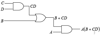
Figure : Logic gate implementation of the expression A (B +CD) .
There are also certain forms of Boolean expressions that are more commonly used than others; the two most important of these are the sum-of-products and the product-of-sum forms.
➤ Sum-of-Product Form
Example: Implement the expression AB + BCD + EFGH with logic gates.
An important characteristic of the sum-of-products form is that the corresponding implementation is always a two-level gate network; that is, the maximum number of gates through which a signal must pass in going from an input to the output is two, excluding inversions.
➤ Product-of-Sums Form
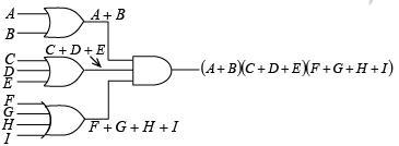
The product-of-sums form can be thought of as the dual of the sum-of-products. It is, in terms of logic functions, the AND of two or more OR functions. For instance, (A + B) (B+ C) is a product-of-sums expression. Several other examples are 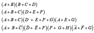
Example: Construct the following function with logic gate.
( A+ B)(C+ D + E)(F + G + H + I)
Simplification of Boolean Expressions
➤ Boolean Algebra Techniques
Example: Simplify the expression AB +A ( B + C )+ B ( B + C) using Boolean algebra techniques.
The following is not necessarily the only approach.
Step1. Apply the distributive law to the second and third terms in the expression, as follows: AB + AB+ AC + BB + BC
Step2. Apply rule 7 ( B.B =B) : AB +AB +AC+ B + BC
Step3. Apply rule 5 ( AB +AB= AB) : AB + AC + B+ BC
Step4. Factor B out of the last two terms: AB + AC+ B (1 + C )
Step5. Apply rule 2 (1 + C=1) : AB +AC + B.1
Step6. Apply rule 4 ( B.1 = B) : AB + AC + B
Step7. Factor B out of the first and third terms, as follows: B ( A + 1)+AC
Step8. Apply rule 2 ( A + 1=1) : B.1 + AC
Step9. Apply rule 4 ( B.1 = B) : B + AC
➤ The Karnaugh Map
The Karnaugh map provides a systematic method for simplifying a Boolean expression and, if properly used, will produce the simplest sum-of-products expression possible. The map format: The Karnaugh map is composed of an arrangement of adjacent “cells”, each representing one particular combination of variables in product form. Since the total number of combinations of n variables and their complements is 2n , the Karnaugh map consists of 2n cells. For example, there are four combinations of the products of two variables ( A and B) and their complements  and AB . Therefore, the Karnaugh map must have four cells, with each cell representing one of the variable combinations, as illustrated in figure (a). The variable combinations are labeled in the cells only for purposes of illustration. In practice, the map is actually arranged with the variables labeled outside the cells, as shown in figure (b). The variable above a column of cells applies to each cell in that column.
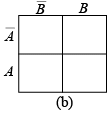 Figure : Format of two-variable Karnaugh map.
Extensions of the Karnaugh map to three and four variables are shown in figure. Notice that the cells are arranged such that there is only a single variable change between any adjacent cells (this is the characteristic that determines adjacency). 
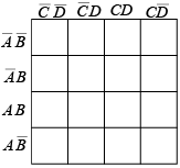
Figure : Formats for three and four-variable Karnaugh maps.
- Plotting a Boolean Expression
Once a Boolean expression is in the sum-of-products form, you can “plot” it on the Karnaugh map by placing 1 in each cell corresponding to a term in the sum-of-products expression. For example, the three-variable expression and the fourvariable expression
  are plotted on the map as shown in figure.
  Figure : Examples of plotting a Boolean expression on a Karnaugh map.
 - Grouping Cells for Simplification
You can group 1s that are in adjacent cells according to the following rules by drawing a loop around those cells:
1. Adjacent cells are cells that differ by only a single variable (for example ABCD and are adjacent).
2. The 1s in adjacent cells must be combined in groups of 1, 2, 4, 8, 16, and so on.
3. Each group of 1s should be maximized to include the largest number of adjacent cells as possible in accordance with rule 2.
4. Every 1 on the map must be included in at least one group. There can be overlapping groups if they include noncommon 1s.
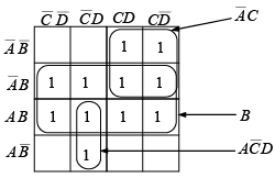
Grouping is illustrated by an example in figure 5.20. Notice how the groups are overlapped to include all the 1s in the largest possible group. Figure : Example of grouping1s on a four-variable Karnaugh map.
 - Simplifying the Expression
When all the 1s representing each term in the original Boolean expression are grouped, the mapped expression is ready for simplification. The following rules apply:
1. Each group of 1s creates a product term composed of all variables that appear in only one form (uncomplemented or complemented) within the group. Variables that appear both uncomplemented and complemented are eliminated.
2. The final simplified expression is formed by summing the product terms of all the groups.
For example, in figure, the product term for the eight-cell group is B because the cells within that group contain both so these variables are eliminated. The four-cell group contains B,
  leaving the product term
  . The two-cell group contains
  leaving
  as the product term. The resulting Boolean expression is the sum of these product terms:

Figure : This plotted Boolean expression simplifies to
Example: Minimize the expression
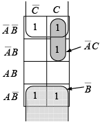
Notice that this expression is already in a sum-of-products form from which the 1s can be plotted very easily, as shown in figure. Four of the 1s appearing in adjacent cells can be grouped. The remaining 1 is absorbed in an overlapping group. The group of four 1s produces a single variableThis is determined by observing that within the group
the only variable that does not change from cell to cell. The group of two 1s produces a two-variable term,
This is determined by observing that within the group, the variables
and C do not change from one cell to the next. To get the minimized function, the two terms that are produced are summed (ORed) as
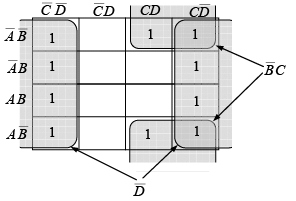
Example: Reduce the following four-variable function to its minimum sum-of-products form:  If all variables and their complements were available, this function would take ten-4-input AND gates and one 10-input OR gate to implement.
A group of eight 1s can be factored as shown in figure because the 1s in the outer columns are adjacent. A group of four 1s is formed by the “wrap-around” adjacency of the cells to pick up the remaining two 1s. The minimum form of the original equation is
takes one 2-input AND gate and one 2-input OR gate. Compare this to the implementation of the original function.
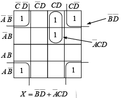
Example: Reduce the following function to its minimum sum-of-products form: 
The function is plotted on the four variable map and factored as indicated in figure. Notice that the four corner cells are adjacent.
- Implementing Truth Table Functions
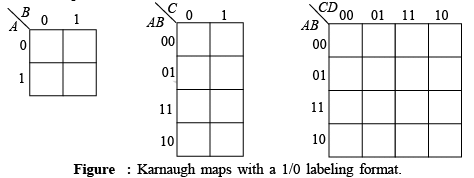
Another use of the Karnaugh map is in implementing logic functions that are specified in truth table format. Since truth tables normally use 1s and 0s (HIGH and LOWs) to represent logic states, the format of the Karnaugh map is modified slightly for this application, as shown in figure for two, three and four variables; 1s and 0s are used to label the cells. The variables represented by the 1s and 0s are specified in the upper left corner of the map.
- Plotting the truth table
When the output variable on the truth table is a 1, a 1 is placed on the Karnaugh map in the cell corresponding to the states of the input variables. For example, if the output variable is a 1 when A = 1 , B = 0 , and C = 1 , then a 1 is placed in the lower right cell of the three-variable map. - Grouping and simplification
The previously stated rules apply in grouping the 1s. Variables that are both 1 and 0 within a group are eliminated. If a variable is a 1 in all cells of a group, it appears uncomplemented in the product term. If a variable is a 0 in all cells of a group, it appears complemented in the product term.
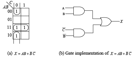
Example: Implement the logic function specified by the truth table using the Karnaugh map method. X is the output variable, and A, B and C are the input variables.
The truth table function is plotted and simplified on the map. The logic gate implementation for the resulting sum-of-products expression is shown in part (b) of the figure. 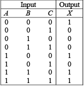
Universal Gates
➤ The Universal Property of the NAND Gate
The NAND gate can be used to generate the NOT function, the AND function, the OR function, and the NOR function.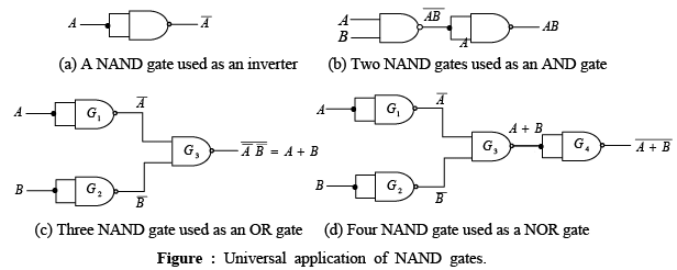
➤ The Universal Property of the NOR Gate
As with the NAND gate, the NOR gate can be used to generate the NOT, AND, OR, and NAND functions. 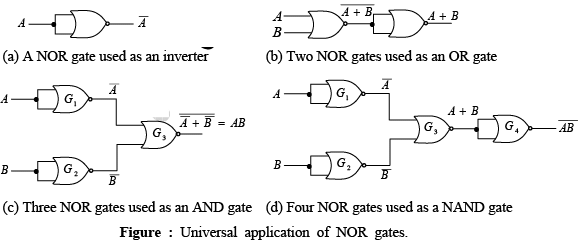
- Pulsed Operation
Example: Determine the output waveform for the circuit in figure (a), with the inputs as shown.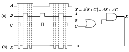
X is shown in the proper time relationship to the inputs in figure (b).
Example: Determine the output waveform for the circuit in figure (a) if the input waveforms are as indicated. 
When both inputs are HIGH or when both inputs are LOW, the output is HIGH. This is called a coincidence circuit or exclusive-NOR. The intermediate outputs of gates G2 and G3 are used to develop the final output.
|
91 videos|21 docs|25 tests
|
FAQs on Digital Electronics - Solid State Physics, Devices & Electronics
| 1. What is digital electronics? |  |
| 2. What is the importance of digital electronics in IIT JAM? |  |
| 3. What are the key topics covered in the digital electronics section of the IIT JAM exam? |  |
| 4. How can I prepare effectively for the digital electronics section of the IIT JAM exam? |  |
| 5. Are there any specific strategies for solving digital electronics questions in the IIT JAM exam? |  |
|
91 videos|21 docs|25 tests
|

|
Explore Courses for Physics exam
|

|




 appearing on the input or output of a logic element, as shown in figure (b) and (d). When appearing on input, it means that an external LOW level produces an internal HIGH. When appearing on the output, it means that an internal HIGH produces an external LOW level. Either indicator (bubble or triangular) can be used on both distinctive shape symbols and rectangular outlines as indicated. The placement of the negation or polarity indicator does not imply a change in the way an inerter operates.


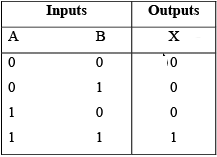
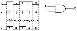 Figure : Example of pulsed AND gate operation.

 Apply K.V.L.


 and change the sign (.to +) between D and


 An important characteristic of the sum-of-products form is that the corresponding implementation is always a two-level gate network; that is, the maximum number of gates through which a signal must pass in going from an input to the output is two, excluding inversions.
 and the fourvariable expression
  are plotted on the map as shown in figure.
 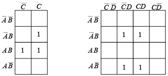 Figure : Examples of plotting a Boolean expression on a Karnaugh map.
 are adjacent).
 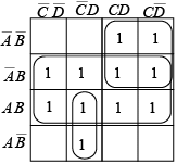 Figure : Example of grouping1s on a four-variable Karnaugh map.
  so these variables are eliminated. The four-cell group contains B,
  leaving the product term
  . The two-cell group contains
  leaving
  as the product term. The resulting Boolean expression is the sum of these product terms:


 This is determined by observing that within the group
  the only variable that does not change from cell to cell. The group of two 1s produces a two-variable term,
  This is determined by observing that within the group, the variables
  and C do not change from one cell to the next. To get the minimized function, the two terms that are produced are summed (ORed) as
 takes one 2-input AND gate and one 2-input OR gate. Compare this to the implementation of the original function.