Previous Year Questions: Microprocessor | Digital Circuits - Electronics and Communication Engineering (ECE) PDF Download
Q.1. The clock frequency of an 8085 microprocessor is 5 MHz. If the time required to execute an instruction is 1.4 μs, then the number of T-states needed for executing the instruction is
(a) 1
(b) 6
(c) 7
(d) 8
Correct Answer is Option (c)
The number of T-states needed for executing the instruction = (Execution time of instruction) x (Clock frequency)
fclock = 5MHz; Tclock = 0.2 x sec (T=1/f)
Texecution = 1.4μs
= 1.4 × 10–6 × 5 × 106
= 7
Q.2. The following FIVE instructions were executed on an 8085 microprocessor.
MVI A, 33H
MVI B, 78H
ADD B
CMA
ANI 32H
The Accumulator value immediately after the execution of the fifth instruction is
(a) 00H
(b) 10H
(c) 11H
(d) 32H
Correct Answer is Option (b)
MVI A, 33H A ← 33H
MVI B, 78H B ← 78H
ADD B B ← ABH
CMA A ← 54H
ANI 32H A ← 10HA → 0011 0011 A → 1010 1011
B → 0111 1000 B → 0101 0100
Q.3. In an 8085 system, a PUSH operation requires more clock cycles than a POP operation. Which one of the following options is the correct reason for this?
(a) for POP, the data transceivers remain in the same direction as for instruction fetch (memory to processor), whereas for PUSH their direction has to be reversed.
(b) Memory write operations are slower than memory read operations in an 8085 based system.
(c) The stack pointer needs to be pre-decremented before writing registers in a PUSH, whereas a
POP operation uses the address already in the stack pointer.
(d) Order of registers has to be interchanged for a PUSH operation, whereas POP uses their natural order.
Correct Answer is Option (c)
In push operation 3 cycles involved: 6T+3T+3T = 127
POP operation 3 cycles involved: 4T+3T+3T = 107
So in the opcode fetch cycle 2T states are extra in case of push compared to POP and this is needed to decrement the SP.
Q.4. In an 8085 microprocessor, the shift registers which store the result of an addition and the overflow bit are, respectively
(a) B and F
(b) A and F
(c) H and F
(d) A and C
Correct Answer is Option (b)
Accumulator stores the result while flag register stores about the overflow.
Shift register are accumulator and flag register (A & F)
Hence B is the correct option.
Q.5. An 8 Kbyte ROM with an active low Chip Select input is to be used in an 8085-microprocessor based system. The ROM should occupy the address range 1000H to 2FFFH.
The address lines are designated as A15 to A0, where A 15is the most significant address bit. Which one of the following logic expressions will generate the correct signal for this ROM?
(a) 
(b) 
(c) 
(d) 
Correct Answer is Option (a)
Address varying from 1000 H to 2FFFH
i.e.
Q.6. In an 8085 microprocessor, the contents of the accumulator and the carry flag are A7 (in hex) and 0, respectively. If the instruction RLC is executed, then the contents of the accumulator (in hex) and the carry flag, respectively, will be
(a) 4E and 0
(b) 4E and 1
(c) 4F and 0
(d) 4F and 1
Correct Answer is Option (d)
Accumulator
RLC → Rotate left accumulator content without carry
Q.7. Which one of the following 8085 microprocessor programs correctly calculates the product of two 8-bit numbers stored in register B and C?
(a) 
(b) 
(c) 
(d) 
Correct Answer is Option (c)
We check the given options.
The codes given in option (C), executes the following instructions
MVI A 00H (loading the accumulator with OOH)
LOOP ADD C (adding the contents of C to accumulator and store it to accumulator)
DCR B (Decrementing the content of registers B)
JNZ LOOP
HLT
Hence, decreasing the number in B as many-time as adding the another number C will result in product of two numbers till value in registers B is zero.
Q.8. In an 8085 microprocessor, which one of the following instructions changes the content of the accumulator?
(a) MOV B, M
(b) PCHL
(c) RNZ
(d) SBI BEH
Correct Answer is Option (d)
Generally arithmetic or logical instructions update the data of accumulator and flags. So, in the given option only SBI BEH is arithmetic instruction.SBI BEH: Add the content of accumulator with immediate data BE H and store the result in accumulator.
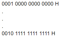
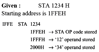
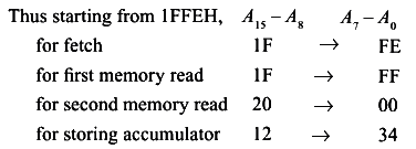
Q.9. An 8085 microprocessor executes “STA 1234H” with starting address location 1FFEH (STA copies the contents of the Accumulator to the 16-bit address location). While the instruction is fetched and executed, the sequence of values written at the address pins A15 - A8 is
(a) 1FH, 1FH, 20H, 12H
(b) 1FH, FEH, 1FH, FFH, 12H
(c) 1FH, 1FH, 12H, 12H
(d) 1FH, 1FH, 12H, 20H, 12H
Correct Answer is Option (a)
STA 1234 does storing value of accumulator at address 1234 H
So, the sequences of values written at the address pins A15 - A8 is
Q.10. For 8085 microprocessor, the following program is executed
MVI A, 05 H;
MVI B, 05H;
PTR: ADD B;
DCR B;
JNZ PTR;
ADI 03H;
HLT;
At the end of program, accumulator contains
(a) 17 H
(b) 20H
(c) 23H
(d) 05H
Correct Answer is Option (a)
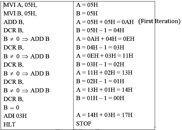
The program is being executed as followsAccumulator changes as follows (05 + 05 + 04 + 03 + 02 + 01) H
At the end of loop accumulator contains = 14H
ADI 03H→ A = (14+03)=17H
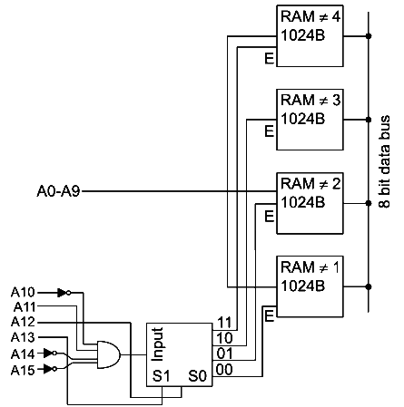
Q.11. There are four chips each of 1024 bytes connected to a 16 bit address bus address bus as shown in the figure below. RAMs, 1, 2, 3, and 4 respectively are mapped to addresses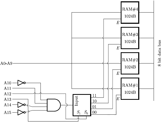
(a) 0C00H–0FFFH. 1C00H-1FFFH. 2C00H-2FFFH, 3C00H-3FFFH
(b) 1800H-1FFFH. 2800H-2FFFH. 3800H-3FFFH. 4800H-4FFFH
(c) 0500H-08FFH, 1500H-18FFH. 3500H-38FFH. 5500H-58FFH
(d) 0800H-0BFFH. 1800H-1BFFH. 2800H-2BFFH. 3800H-3BFFH
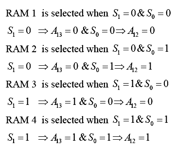
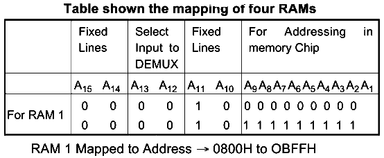
Correct Answer is Option (d)
Q.12. A controller that takes control of the buses and transfers data directly between source and destination bypassing the microprocessor is known as
(a) DMA controller
(b) read-write controller
(c) high-speed controller
(d) master-slave controller
Correct Answer is Option (a)
Direct Memory Access:
The data transfer between a fast storage media such as magnetic disk and memory unit is limited by the speed of the CPU. Thus we can allow the peripherals directly communicate with each other using the memory buses, removing the intervention of the CPU. This type of data transfer technique is known as DMA or direct memory access. During DMA the CPU is idle and it has no control over the memory buses. The DMA controller takes over the buses to manage the transfer directly between the I/O devices and the memory unit
Q.13. A 2-byte instruction which accepts the data from the input port specified in the second byte and loads into the accumulator is
(a) OUT <8-bit port address>
(b) IN <8-bit port address>
(c) OUT R<8-bit port address>
(d) IN R < 8-bit port address>
Correct Answer is Option (b)
IN (8-bit port address) 1 byte is for opcode and 1 byte for 8 bit port address so it is a 2 Byte instruction and this instruction is used to accept the data from the inport port and load this data into accumulator.
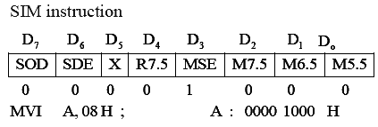
Q.14. Consider the following instruction:
El
MVl A, 08H
SlM
It means
(a) disable all interrupts
(b) enable all interrupts
(c) disable RST 7.5 and 6.5
(d) enable RST 7.5 and 6.5
Correct Answer is Option (b)
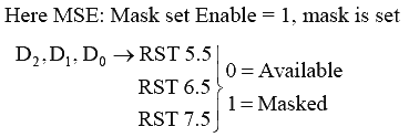
EI → means enable all maskable interrupts
MVI A, 08H → load accumulator with 08H
SIM → set interrupt mask
∴ Data of A is copied to 5IM
A has (0000 1000)2
But RST 7.5, 6.5 & 5.5 are not masked
therefore Given instruction enable all interrupts
Q.15. The instruction BC 0X15 means
(a) jump 15 bytes relative to the program counter
(b) copy and load 15 words in reverse direction to the program counter
(c) move to a location by 15 bits to the program counter
(d) redirect (jump) to a location by 15 words relative to the program counter
Correct Answer is Option (a)
Micro processor does not have any instruction such as BC so it is a printing mistake
It should be JC OX 15 which means jump by 15 bytes if carry is zero relative to program counter.
Q.16. Which of the following constraints are to be considered by the designer while designing an embedded system?
1) Selecting the microcontroller as a controlling device
2) Selecting the language to write the software
3) Partitioning the tasks between hardware and software to optimize the cost
Select the correct answer using the code given below
(a) 1, 2 and 3
(b) 1 and 2 only
(c) 1 and 3 only
(d) 2 and 3 only
Correct Answer is Option (a)
Following constraints are to be considered by the designer while designing an embedded system :
Microcontroller is selected as controlling device
Language is selected to write the program (software) without difficulties.
Partioning the tasks between hardware and software to optimize the case.
Q.17. The following six (6) items consist of two statements, one labelled as ‘Statement (I)’ and the other as ‘Statement (II)‘. You are to examine these two statements carefully and select the answers to these items using the code given below:
Statement (I): Sign-magnitude representation is rarely used in implementing the integer of the ALU.
Statement (II): There are two representations of zero in sign-magnitude representation.
(a) Both Statement (I) and Statement (II) are individually true and Statement (II) is the correct explanation of Statement (I)
(b) Both Statement (I) and Statement (II) are individually true but Statement (II) is not the correct explanation of Statement (I)
(c) Statement (I) is true but Statement (II) is false
(d) Statement (I) is false but Statement (II) is true
(e) None
Correct Answer is Option (e)
In modern computer system 2’s complement representation is used.
1) In sign magnitude form and 1’s complement form, the disadvantage is ‘0’ has two representations.
2) Only 2’s complement form has unique representation of 0. Hence 2’s complement form is preferred.
In sign-magnitude format, MSB decides the sign. If MSB is 0 then sign is positive and if MSB is 1, then sign is negative (i.e. number is negative)
e.g. For 3 bit sign magnitude representation
000 -> +0
100 -> -0
Hence statement (II) is correct explanation of statement (I).
1. Signed Magnitude Method:
In the signed magnitude method number is divided into two parts: Sign bit and magnitude. Sign bit is 1 for negative number and 0 for positive number. Magnitude of number is represented with the binary form of the number.2. 2’s Complement Method:
In 2’s complement method, positive numbers are represented in the same way as they are represented in sign magnitude method. But if the number is negative, first represent the number with positive sign and then take 2’s complement of that number.
Q.18.
VHDL
entity test is
port
(
data : in std_logic;
clk : in std_logic;
rset : in std_logic;
q : out std_logic
);
end test;
architcture behav of test is
begin
process (clk)
begin
if (clk’event and clk =’1’) then
if (reset =’0’) then
q <= ‘0’;
else
q <= data;
end if;
end if;
end process;
end behav;
VERILOG
module test (data, clk, reset, q);
input data, clk, reset;
output q;
reg q;
always @ (posedge clk)
if (reset)
q = 1’b0;
else q = data;
endmodule
The Above Verilog/VHDL module depicts which sequential element:
(a) Rising edge Flip-flop with synchrounus Reset
(b) Falling edge Flip-flop with synchrounus Reset
(c) Rising edge Flip-flop with asynchrounus Reset
(d) Falling edge Flip-flop with asynchrounus Reset
Correct Answer is Option (a)
in the given programming , ‘if’ condition is used to check occurrence of rising edge . and as RESET is used with every clock cycle that indicates it is synchronous.
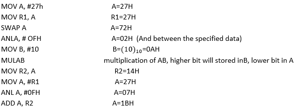
Q.19. What is the content of Accumulator in binary after execution of following 8051 Assembly code:
MOV A, #27h
MOV R1, A
SWAP A
ANLA, # OFH
MOV B, #10
MULAB
MOV R2, A
MOV A, #R1
ANL A, #0FH
ADD A, R2
(a) 00011011
(b) 01110010
(c) 01010101
(d) 11001011
Correct Answer is Option (a)
The Correct Answer Among All the Options is A
Q.20. In a 16-Bit micro-controller if a two-dimensional integer array A[5][7] is stored at base location 0x8000, What is the address of A[4][2]?
(a) 0x800C
(b) 0x803C
(c) 0x801F
(d) 0x840
Correct Answer is Option (b)
The Correct Answer Among All the Options is B
microcontroller follows byte addressing storage method, even though it is 16-bit controller ,each address location stores only 1 bye.
Given 2’Dimensional array A[5][7] has total of 5 rows and 7 column. Array will be stored in memory by each row wise. Each row is having 7 elements , each of 2 bytes (16bits), which requires total of 14bytes(72).
Q.21. Content of variable flag after following ‘C’ code execution:
Unsigned char flag = 0x7C;
flag=flag | 0x80;
flag=flag | (1<<4);
flag&=~(1<<7);
flag^=(1<<6);
(a) 0x1C
(b) 0x20
(c) 0x24
(d) 0x3C
Correct Answer is Option (d)
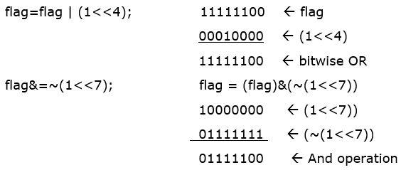
Unsigned char flag = 0x7C;
flag=01111100
flag=flag | 0x80;
it is bitwise OR operation.
Flag =00111100=0x3C
Q.22. Process P1, P2 and P3 with execution time of 6 ms, 4 ms and 2 ms respectively enter in ready state together in order P1, P2, P3. Calculate the waiting and turnaround time of Process P1. Assuming no wait time due to I/O and round scheduling with time slot of 2 ms.
(a) 6 ms, 12ms
(b) 6 ms, 10 ms
(c) 4 ms, 4 ms
(d) 4 ms, 6 ms
Correct Answer is Option (a)
Round robin is a CPU scheduling algorithm where each process is assigned a fixed time slot in a cyclic way.
Turnaround time (TAT) is the time interval from the time of submission of a process to the time of the completion of the process. It can also be considered as the sum of the time periods spent waiting to get into memory or ready queue, execution on CPU and executing input/output.
Q.23.
A) HDL Coding /RTL Design
B) Synthesis
C) Static Timing Analysis
D) Place and Route
E) Programming file generation
What is the correct order of FPGA design flow?
(a) A,B,C,D,E
(b) A,B,D,C,E
(c) B,D,C,E,A
(d) C,A,D,E,B
Correct Answer is Option (b)
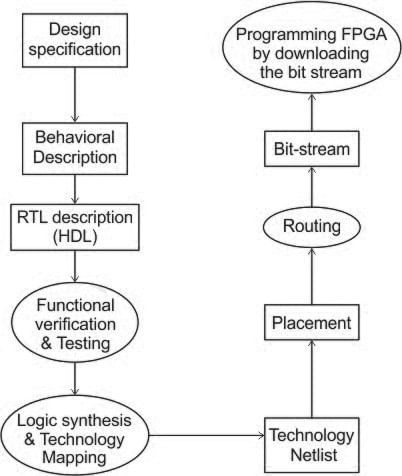
Field Programmable Gate Array (FFGA) is a device that has a numerous gate (switch) arrays. The contents of the memory of FPGA is erased once the power is turned off.
The FFGA design flow is explained with the help of the following flow diagram:
So, Option (2) indicates the correct order.
Q.24. Which of these is non-operational attribute of embedded system?
(a) Response
(b) Throughput
(c) Security
(d) Portability
Correct Answer is Option (d)
Operational Quality Attributes.: These are attributes related to operation or functioning of an embedded system. The way an embedded system operates affects its overall quality. Some of the Operational Attributes are:
- Response
- Throughput
- Reliability
- Maintainability
- Security
- Safety
Non Operational Attributes: These are attributes not related to operation or functioning of an embedded system. The way an embedded system operates affects its overall quality.These are the attributes that are associated with the embedded system before it can be put in operation. Some of non-operational attributes are:
- Testability and Debug-ability
- Evolvability
- Portability
- Time to prototype and market
- Per unit and total cost
Q.25. For the below mentioned 8051 assembly code
Time elapse : MOV R0, #100
Part 1 : MOV R1, #50
Part 2 : MOV R2, #248
Part 3 : DJNZ R2, Part3
: DJNZ R1, Part2
: DJNZ R0, Part1
Assumptions:
- Microcontroller is running at 12 MHz frequency and 1 machine cycle is having 12 clock cycles
- MOV instruction takes 1 Machine cycle
- DJNZ instruction takes 2 Machine cycle
Calculate time required for execution of Part 1
(a) 2495600
(b) 2496300
(c) 2495300
(d) 2496600
Correct Answer is Option (c)
The Correct Answer Among All the Options is C
calculation of execution time for part-3:
Code in part will be executed 248 times, so part3 execution time is
=248 x 2 machine cycle{ bcz DJNZ instruction takes 2 machine cycle}
=248 x 2 x 1 μs
= 496 μs
Code in part 2 will executed 50 times. So execution time for part 2 is
=50[1]
=50(499)
Code in part 1 will executed 100 times. So execution time for part 1 is
=100[1 +50(499)+2]
=2495300
|
76 videos|175 docs|70 tests
|


