Zener Diodes | Electronic Devices - Electronics and Communication Engineering (ECE) PDF Download
Introduction
A Zener diode not only allows current to flow from anode to cathode but also, in the reverse direction on reaching the Zener voltage. Due to this functionality, Zener diodes are the most commonly used semiconductor diodes. In this article, let us learn the function of Zener diodes along with its construction, operation and more.
Zener Diode Explanation
A Zener Diode, also known as a breakdown diode, is a heavily doped semiconductor device that is designed to operate in the reverse direction. When the voltage across the terminals of a Zener diode is reversed and the potential reaches the Zener Voltage (knee voltage), the junction breaks down and the current flows in the reverse direction. This effect is known as the Zener Effect.
Zener Diode Definition
A Zener diode is a heavily doped semiconductor device that is designed to operate in the reverse direction.
Zener diodes are manufactured with a great variety of Zener voltages (Vz) and some are even made variable.
History of Zener Diodes
Clarence Melvin Zener was the first person to describe the electrical properties of Zener Diode. Clarence Zener was a theoretical physicist who worked at Bell Labs. As a result of his work, the Zener diode was named after him. He first postulated the breakdown effect that bears his name in a paper that was published in 1934.
How does a Zener Diode work in reverse bias?
A Zener diode operates just like a normal diode when it is forward-biased. However, a small leakage current flows through the diode when connected in reverse biased mode. As the reverse voltage increases to the predetermined breakdown voltage (Vz), current starts flowing through the diode. The current increases to a maximum, which is determined by the series resistor, after which it stabilizes and remains constant over a wide range of applied voltage.
There are two types of breakdowns for a Zener Diode:
- Avalanche Breakdown
- Zener Breakdown
1. Avalanche Breakdown in Zener Diode
Avalanche breakdown occurs in normal diode and Zener Diode at high reverse voltage. When a high value of reverse voltage is applied to the PN junction, the free electrons gain sufficient energy and accelerate at high velocities. These free electrons moving at high velocity collide with other atoms and knock off more electrons. Due to this continuous collision, a large number of free electrons are generated as a result of electric current in the diode rapidly increases. This sudden increase in electric current may permanently destroy the normal diode. However, a Zener diode is designed to operate under avalanche breakdown and can sustain the sudden spike of current. Avalanche breakdown occurs in Zener diodes with Zener voltage (Vz) greater than 6V.
2. Zener Breakdown in Zener Diode
When the applied reverse bias voltage reaches closer to the Zener voltage, the electric field in the depletion region gets strong enough to pull electrons from their valence band. The valence electrons that gain sufficient energy from the strong electric field of the depletion region break free from the parent atom. At the Zener breakdown region, a small increase in the voltage results in the rapid increase of the electric current.
Avalanche Breakdown vs Zener Breakdown
- The Zener effect is dominant in voltages up to 5.6 volts and the avalanche effect takes over above that.
- They are both similar effects, the difference being that the Zener effect is a quantum phenomenon and the avalanche effect is the movement of electrons in the valence band like in any electric current.
- Avalanche effect also allows a larger current through the diode than what a Zener breakdown would allow.
Circuit Symbol of Zener Diode
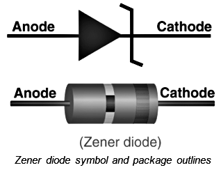
There are many ways in which a Zener diode is packaged. Some are used for high levels of power dissipation and the others are contained with surface mount formats. The most common Zener diode type is contained within a small glass encapsulation. It has a band around one end marking the cathode side of the diode.

From the diagram, we can see that the band around the package corresponds to the line on the diode circuit symbol and this can be an easy way of remembering which end is for which.
The Zener diode circuit symbol places two tags at the end of the bar – one in the upward direction and the other in the lower direction, as shown in the figure. This helps in distinguishing Zener diodes from other forms of diodes within the circuit.
V-I Characteristics of Zener Diode
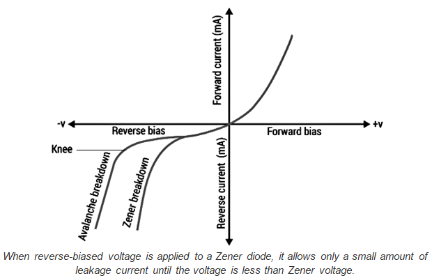
The diagram given below shows the V-I characteristics of the Zener diode.

The V-I characteristics of a Zener diode can be divided into two parts as follows:
- Forward Characteristics
- Reverse Characteristics
1. Forward Characteristics of Zener Diode
The first quadrant in the graph represents the forward characteristics of a Zener diode. From the graph, we understand that it is almost identical to the forward characteristics of any other P-N junction diode.
2. Reverse Characteristics of Zener Diode
When a reverse voltage is applied to a Zener voltage, a small reverse saturation current Io flows across the diode. This current is due to thermally generated minority carriers. As the reverse voltage increases, at a certain value of reverse voltage, the reverse current increases drastically and sharply. This is an indication that the breakdown has occurred. We call this voltage breakdown voltage or Zener voltage, and Vz denotes it.
Zener Diode Specifications
Some commonly used specifications for Zener diodes are as follows:
- Zener/Breakdown Voltage: The Zener or the reverse breakdown voltage ranges from 2.4 V to 200 V, sometimes it can go up to 1 kV while the maximum for the surface-mounted device is 47 V.
- Current Iz (max): It is the maximum current at the rated Zener Voltage (Vz – 200μA to 200 A)
- Current Iz (min): It is the minimum value of current required for the diode to breakdown.
- Power Rating: It denotes the maximum power the Zener diode can dissipate. It is given by the product of the voltage of the diode and the current flowing through it.
- Temperature Stability: Diodes around 5 V have the best stability
- Voltage Tolerance: It is typically ±5%
- Zener Resistance (Rz): It is the resistance to the Zener diode exhibits.
Application of Zener Diode
Following are the applications of Zener diode:
- Zener diode as a voltage regulator: Zener diode is used as a Shunt voltage regulator for regulating voltage across small loads. The Zener diode is connected parallel to the load to make it reverse bias, and once the Zener diode exceeds knee voltage, the voltage across the load will become constant. The breakdown voltage of Zener diodes will be constant for a wide range of currents.
- Zener diode in over-voltage protection: When the input voltage is higher than the Zener breakage voltage, the voltage across the resistor drops resulting in a short circuit, this can be avoided by using the Zener diode.
- Zener diode in clipping circuits: Zener diode is used for modifying AC waveform clipping circuits by limiting the parts of either one or both the half cycles of an AC waveform.
|
38 docs|29 tests
|


