Conversion of Flip-Flops

In the previous chapter we studied the four basic flip‐flops: SR, D, JK and T flip‐flops. Any one of these can be realised from another by adding suitable combinational logic to convert input signals so that the given flip‐flop exhibits the characteristic behaviour of the desired flip‐flop. There are twelve possible one‐stage conversions (each flip‐flop to the other three).
General procedure for converting one flip‐flop into another:
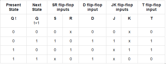
- Write the characteristic table of the desired flip‐flop (the table that defines its next state Q(t + 1) in terms of present state Q(t) and its inputs).
- Use the excitation table of the given (available) flip‐flop to find the required input values of that flip‐flop which will produce the desired next state for every combination of present state and desired next state.
- Simplify the Boolean expressions for the excitation inputs using algebra or Karnaugh maps.
- Draw the final circuit by connecting the simplified combinational logic to the inputs of the given flip‐flop. Verify that for each present state and external input the next state matches the desired flip‐flop behaviour.
SR Flip‐Flop to other flip‐flops
Using an SR flip‐flop as the available device we can obtain the other three flip‐flops by providing appropriate logic at S and R. The three conversions are:
- SR → D
- SR → JK
- SR → T
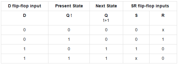
SR → D flip‐flop
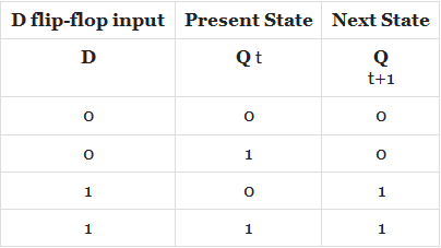
Desired characteristic: for a D flip‐flop, Q(t + 1) = D.
Use the excitation table of the SR flip‐flop to find S and R required for each present and next state. The filled table for D characteristic appears as shown below.
Simplify S and R using K‐maps (two‐variable K‐maps are adequate here).
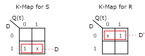
The simplified results are
S = D
R = D'
The implementation is therefore an SR flip‐flop with the input D applied to S and the inverted D applied to R. The circuit diagram is:
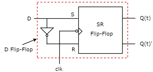
This circuit has a single external input D and outputs Q(t) and Q(t)'. The inverter produces D', so S and R always take complementary values and the invalid S = R = 1 condition never occurs.
SR → JK flip‐flop
Desired characteristic: for a JK flip‐flop, Q(t + 1) = J Q'(t) + K' Q(t).
We must choose S and R (inputs to the SR device) as functions of J, K and Q so that the SR next state equals the JK next state for every Q, J and K.
Constructing the truth table and simplifying gives the standard excitation mappings
S = J Q' + K' Q
R = J' Q' + K Q
These expressions ensure that for each present state Q and external inputs J,K the SR flip‐flop receives the correct S and R to produce the same Q(t + 1) as the JK characteristic.
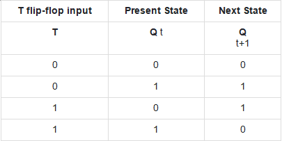
SR → T flip‐flop
Desired characteristic: for a T flip‐flop, Q(t + 1) = Q(t) ⊕ T.
To make an SR device toggle when T = 1 and hold when T = 0, provide S and R that set or reset depending on current Q and T. The standard mapping is
S = T · Q'
R = T · Q
When T = 0, S = R = 0 so the SR device holds. When T = 1, S = Q' and R = Q so the SR device complements Q, achieving the toggle action.
D Flip‐Flop to other flip‐flops
Using a D flip‐flop as the available device we can obtain the other three flip‐flops by providing appropriate logic that drives the single input D. The three conversions are:
- D → T
- D → SR
- D → JK
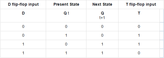
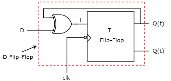
D → T flip‐flop
Desired characteristic: T flip‐flop.
Fill the D excitation table for each present Q and desired Q(t + 1) given by the T characteristic. The filled table and result are shown below.
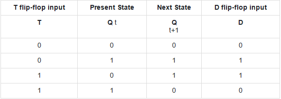
The Boolean function for D that implements T behaviour is
D = T ⊕ Q(t)
Thus the circuit is a D flip‐flop with an Exclusive‐OR gate combining T and Q(t) to generate D:
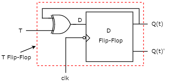
When T = 0, D = Q and the D flip‐flop holds; when T = 1, D = Q' and the D flip‐flop toggles.
D → SR flip‐flop
Desired characteristic: SR. The D input must be a function of SR and Q so that Q(t + 1) = D = SR behaviour.
From the SR truth table the required D expression is
D = S + Q · R'
Check:
- If S = 1, D = 1 (set).
- If R = 1 and S = 0, D = 0 (reset).
- If S = R = 0, D = Q (hold).
Use this logic to drive the single D input of the D flip‐flop so that it emulates an SR device.
D → JK flip‐flop
Desired characteristic: JK. The required next state Q(t + 1) for JK is J Q' + K' Q, and the D input must equal that value. Therefore
D = J · Q' + K' · Q
This expression is implemented with combinational logic feeding the D input of the D flip‐flop. The D device then produces the same next state as a JK flip‐flop would for inputs J and K.
JK Flip‐Flop to other flip‐flops
Using a JK flip‐flop as the available device we can obtain the other three flip‐flops by driving J and K appropriately. The three conversions are:
- JK → T
- JK → D
- JK → SR
JK → T flip‐flop
Desired characteristic: T.
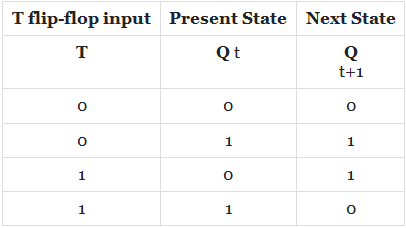
Fill the JK excitation table for T characteristic as in the figure below.
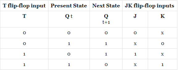
Simplification gives the simple connection
J = T
K = T
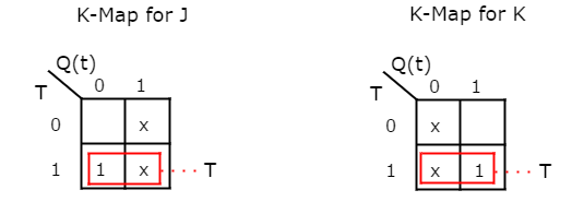
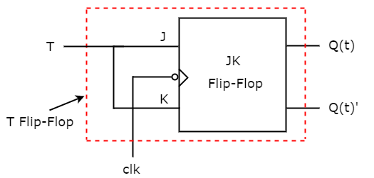
Thus connect the same input T to both J and K. When T = 0 both J and K are 0 and the JK holds; when T = 1 both are 1 and JK toggles, producing T behaviour.
JK → D flip‐flop
Desired characteristic: D. Choose J and K as functions of D so that Q(t + 1) = D.
Set
J = D
K = D'
Then Q(t + 1) = J Q' + K' Q = D Q' + (D')' Q = D(Q' + Q) = D, so the JK device behaves exactly as a D flip‐flop. Only one inverter is required.
JK → SR flip‐flop
Desired characteristic: SR. We must choose J and K so that the JK next state equals the SR next state. A correct and commonly used mapping is
J = S · Q'
K = R · Q
With these connections, for each present state Q and external SR inputs the JK device yields the same next state as that required by the SR flip‐flop (for the valid SR input combinations).
T Flip‐Flop to other flip‐flops
Using a T flip‐flop as the available device we can obtain the other three flip‐flops by providing suitable logic to its single input T. The three conversions are:
- T → D
- T → SR
- T → JK
T → D flip‐flop
Desired characteristic: D.
The required relation between T and D is obtained from Q(t + 1) = D and Q(t + 1) = Q ⊕ T. Equate these to get
T = D ⊕ Q(t)
Thus an Exclusive‐OR of D and Q drives the T input of the T flip‐flop so that the device behaves as a D flip‐flop.
T → SR flip‐flop
Desired characteristic: SR. We need a single T input that makes the T flip‐flop produce the SR next state for every present Q and external S,R. Starting from
Q(t + 1) = S + Q · R'
and Q(t + 1) = Q ⊕ T, solve for T to obtain
T = S · Q' + R · Q · S'
This expression ensures that when the SR inputs indicate set/reset/hold, the single T input will make the T device behave equivalently.
T → JK flip‐flop
Desired characteristic: JK. Equate Q(t + 1) expressions and solve for T. The resulting simplified expression is
T = J · Q' + K · Q
Use this logic to feed the T input of the T flip‐flop. When J and K are provided externally, this T input makes the T flip‐flop replicate the JK behaviour.
Practical notes and verification
- When converting between flip‐flops always check the forbidden or invalid input combinations. For example, SR has S = R = 1 as invalid; conversions should ensure this condition does not arise at the physical SR inputs for valid external input combinations.
- Simplify expressions using Karnaugh maps or Boolean algebra to minimise gate count and avoid hazards where possible.
- After designing the combinational logic, verify the complete truth table (for all combinations of present state and external inputs) to ensure Q(t + 1) matches the desired flip‐flop characteristic.
- Where possible prefer mappings that use fewer gates or avoid producing forbidden input combinations at the underlying flip‐flop.
Summary
The conversion procedure uses the characteristic table of the desired flip‐flop together with the excitation table of the available flip‐flop to obtain Boolean expressions for the excitation inputs. Each conversion yields simple, commonly used expressions:
- SR → D : S = D, R = D'
- SR → JK : S = J Q' + K' Q, R = J' Q' + K Q
- SR → T : S = T Q', R = T Q
- D → T : D = T ⊕ Q
- D → SR : D = S + Q R'
- D → JK : D = J Q' + K' Q
- JK → T : J = T, K = T
- JK → D : J = D, K = D'
- JK → SR : J = S Q', K = R Q
- T → D : T = D ⊕ Q
- T → SR : T = S Q' + R Q S'
- T → JK : T = J Q' + K Q
Use the step‐by‐step procedure and the excitation table (see above) to derive, simplify and implement any conversion needed. Always test the final circuit by comparing its present‐state to next‐state behaviour with the desired characteristic table.


 | Explore Courses for Computer Science Engineering (CSE) exam |
 | Get EduRev Notes directly in your Google search |