Noise Margin & Fan-Out | Digital Electronics - Electrical Engineering (EE) PDF Download
Fan Out of Logic Gates

Key learnings:
- Fan Out Definition: Fan out in digital electronics is the maximum number of inputs a single logic gate output can drive without causing errors.
- Current Sourcing and Sinking: Logic gates must source or sink current based on their high or low output state to drive other gates.
- Fan Out Calculation: Fan out is IOH/IIH when the output is high and IOL/IIL when the output is low, ensuring the logic gate can drive multiple inputs.
- Circuit Design Importance: Proper fan out ensures that circuits function correctly without overloading any logic gate, which is essential in circuit design.
- TTL Logic Family: TTL logic gates have specific fan out values that must be considered when designing circuits.
In digital electronics, we have learned about different types of logic gates and how they work. Now, let’s discuss “fan out,” which relates to logic gates. Fan out refers to how one logic gate’s output can connect to multiple inputs of other gates.
However, there is a limit to the number of inputs that a single logic gate output can handle. This limit depends on the current sourcing capability when the output is high and the current sinking capability when the output is low. It also depends on the current requirements of the connected inputs.

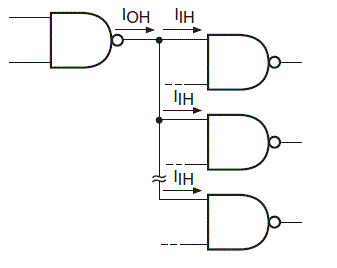
We can illustrate the point further with an example and the diagram above.
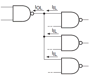
Suppose the current sourcing capability of a NAND gate is IOH when the output of it is in logic high and the inputs of the logic gates which are fed from the output of this logic gate is IIH. We can see this in the diagram also. Now the maximum number of inputs which this output of the logic gate will be able to drive is IOH/ IIH. This will be applicable when the when that output will be in high state. Now considering the case when the output is in the state of logic LOW then the let us take the maximum current sinking capability as IOL. And then again just as the previous one the sinking current which is fed to all the connected inputs of various logic gates is IIL. We are going to show this in the next diagram.

Now for this case the maximum number of input drives which will be driven by the output of that logic gate will be equal to IOL / IIL. So we have found that the maximum number of logic gate inputs that can be fed from the output of a single logic gate will be IOH / IIH when the logic is high and it will be IOL / IIL when the logic is in low state.
The number of logic gate inputs that a single gate output can drive is called the fan out. This is important for designing circuits without causing false outputs. Fan out is a key characteristic in digital electronics.
Now in many cases the values of IOH/IIHand IOL / IIL are different, in that case the smaller of the two is taken as Fan Out of Logic Gates and all the calculations are done based on that value.

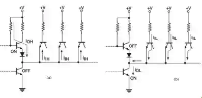
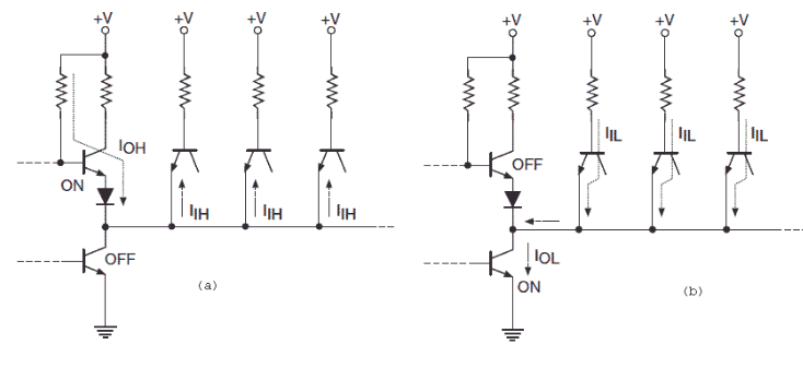
The above two figures show the actual circuit diagram of a circuit where the output of a single NAND gate which belongs to a standard TTL (Transistor Transistor Logic) logic family feeds the inputs of various NAND gate which belongs to the same logic family.
The first figure is for the state when the logic is high and the second figure is during the logic low state. For standard TTL family devices the maximum high state output sourcing current and the maximum high state input current are 400 mu A and 40 mu A respectively. The same values for low state are 16 μ A and 1.6 μ A respectively. We have discussed about the TTLs in other article.
|
113 videos|91 docs|58 tests
|
FAQs on Noise Margin & Fan-Out - Digital Electronics - Electrical Engineering (EE)
| 1. What is fan-out in the context of logic gates? |  |
| 2. How does fan-out affect the noise margin of a logic gate? |  |
| 3. Why is it important to consider fan-out when designing digital circuits? |  |
| 4. What factors can influence the fan-out of a logic gate? |  |
| 5. How can designers optimize fan-out in digital circuits to improve performance? |  |


