Previous Year Questions- Operational Amplifiers - 1 | Analog and Digital Electronics - Electrical Engineering (EE) PDF Download
Q1: A difference amplifier is shown in the figure. Assume the op-amp to be ideal. The CMRR (in dB) of the difference amplifier is _____(rounded off to 2 decimal places). (2024)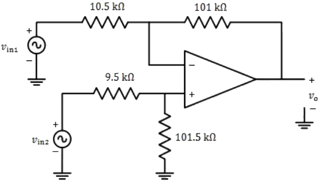 (a) 12.36
(b) 36.25
(c) 40.52
(d) 48.44
Ans: (c)
Sol: 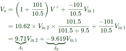 CMRR = Ad/Ac
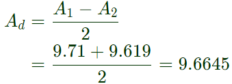 Ac = A1 + A2
= 9.71 - 9.619 = 0.091
CMRR = (9.6645/0.091) = 106.20
CMRR = 20log(106.20) = 40.52 dB
Q2: The current gain (Iout/Iin) in the circuit with an ideal current amplifier given below is (2022)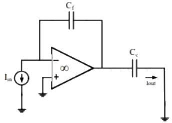 (a) Cf/Cc
(b) -Cf/Cc
(c) Cc/Cf
(d) -Cc/Cf
Ans: (c)
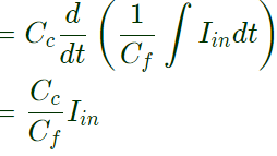
Sol: Redraw the circuit: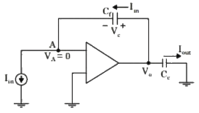 From circuit,
Vo = Vc


Q3: The output impedance of a non-ideal operational amplifier is denoted by Zout. The variation in the magnitude of Zout with increasing frequency, f, in the circuit shown below, is best represented by (2022)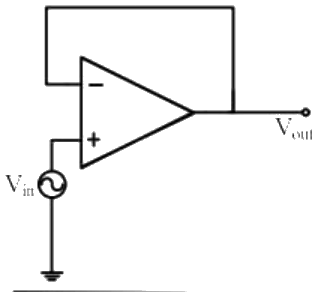 (a)
(a) 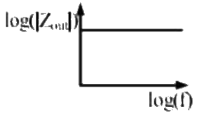 (b)
(b) 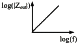 (c)
(c) 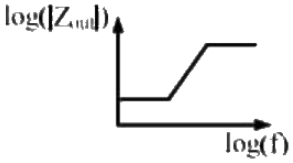 (d)
(d) 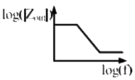 Ans: (c)
Sol: Bode plot of negative feedback amplifier: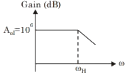 Given amplifier is a voltage series feedback amplifier.
Therefore, Output impedance is given by From Bode plot ; at low frequency, the open loop gain (A) is constant.
when ω↑, A↓, Zout↑
At A = 0, Zout = Zo → constant
Therefore, zout with frequency represented by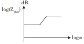
Q4: The steady state output (Vout), of the circuit shown below, will (2022)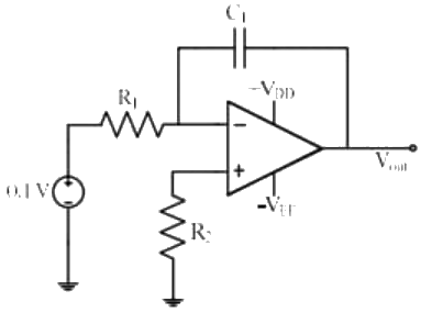 (a) saturate to +VDD
(b) saturate to −VEE
(c) become equal to 0.1 V
(d) become equal to -0.1 V
Ans: (b)
Sol: Redraw the circuit: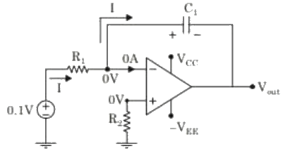 From circuit,
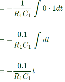
 Hence, Vout = −VEE
Q5: A CMOS Schmitt-trigger inverter has a low output level of 0 V and a high output level of 5 V. It has input thresholds of 1.6 V and 2.4 V. The input capacitance and output resistance of the Schmitt-trigger are negligible. The frequency of the oscillator shown is ____________ Hz. (Round off to 2 decimal places.) (2021)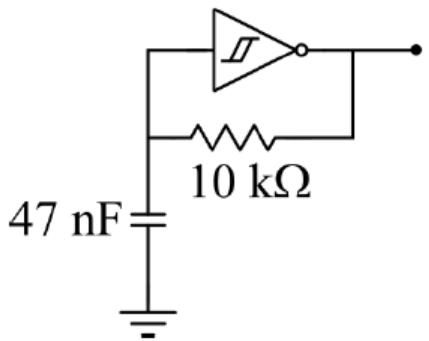 (a) 1245.23
(b) 3157.56
(c) 258.36
(d) 965.24
Ans: (b)
Sol:  vc(t) = vc final +[vinitial −vc′ final] e−t/RC
Charging, vc(t) = 5 + (1.6 − 5)e−t/RC
= 5 − 3.4e−t/RC
t = t1, vc(t) = 2.4 V
2.4 = 5 - 3.4e -t/RC
3.4e-11/RC = 2.6 Discharging,
vc(t) = 0 + (2.4 − 0)e−t/RC
= 2.4e−t/RC
t = t2, vc(ta) = 1.6 V
1.6 = 2.4e−12/AC
t2 = In (2.4/1.6) RC = 0.405 × RC
T = t1 + t2 = (0.268 + 0.405) RC
T = 0.673RC f = 3157.46 Hz
Q6: The temperature of the coolant oil bath for a transformer is monitored using the circuit shown. It contains a thermistor with a temperature-dependent resistance, Rthermistor = 2(1 + αT)kΩ. Where T is the temperature in °C. The temperature coefficient α, is −(4 ± 0.25)%/°C. Circuit parameters: R1 = 1kΩ, R2 = 1.3kΩ, R3 = 2.6kΩ. The error in the output signal (in V. rounded off lo 2 decimal places) at 150°C is ________. (2020)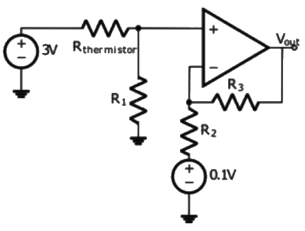 (a) 0.01
(b) 0.08
(c) 0.04
(d) 0.06
Ans: (c)
Sol: As per GATE official answer key MTA (Marks to ALL)
Given data,
Rthermistor = Rth = 2(1 + αT)KΩ
α = −(4 + 0.25)%/°C = −(0.04 ± 0.0025)°C
αmax = −0.0424/°C, αmin = −0.375/°C
Temperature, T = 150°C
R1 = 1KΩ, R2 = 1.3KΩ, R3 = 2.6KΩ
Considering, α = -0.04
Rth = 2[1 − 0.04 × 150] = −10KΩ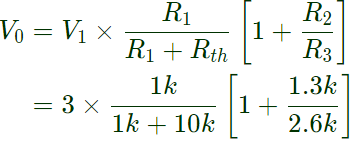 = −0.5V
Case-1:
Considering, αmax = −0.0425/°C
Rthmax = 2[1 + (-0.0425) x 150] = -10.75 kΩ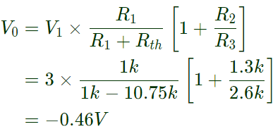 Case-2:
Considering, αmax = −0.0375/°C
Rthmax = 2[1 + (-0.0375) x 150] = -9.25 kΩ = -0.54 V
Output voltage, V0 = 0.5 ± 0.04 ⇒ Error = 0.04
Q7: A common-source amplifier with a drain resistance, RD = 4.7kΩ, is powered using a 10 V power supply. Assuming that the transconductance, gm, is 520μA/V, the voltage gain of the amplifier is closest to: (2020)
(a) -2.44
(b) -1.22
(c) 1.22
(d) 2.44
Ans: (a)
Sol: Given data:
RD = 4.7KΩ, gm = 520μA/V
Voltage gain of CS amplifier
= −gmRD = −520μA/V × 4.7kΩ = −2.44
Q8: In the circuit below, the operational amplifier is ideal. If V1 = 10 mV and V2 = 50 mV, the output voltage (Vout) is (2019)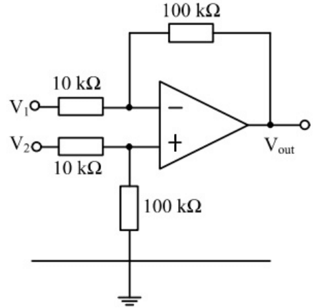 (a) 100 mV
(b) 400 mV
(c) 500 mV
(d) 600 mV
Ans: (b)
Sol: 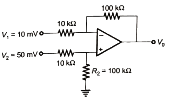 V0 = R2/R1 (V2 - V1)
= 100k/10k (50mV - 10mV)
= 10(40 mV) = 400 mV
Q9: The op-amp shown in the figure is ideal. The input impedance vin/iin is given by (2018)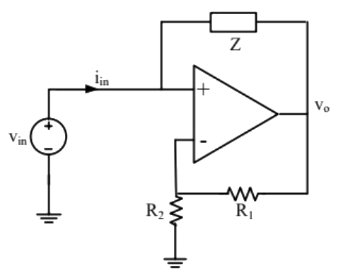 (a) Z(R1/R2)
(b) -Z(R1/R2)
(c) Z
(d) Z(R1/(R1+R2))
Ans: (b)
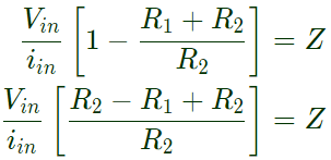
Sol: According to virtual ground,
VA = VB = Vin
At node A,


 Equation (ii) in euation (i),


Q10: For the circuit shown below, assume that the OPAMP is ideal.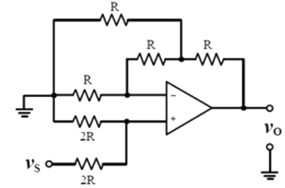 Which one of the following is TRUE? (SET-2(2017))
(a) vo = vs
(b) vo = 1.5vs
(c) vo = 2.5vs
(d) vo = 5vs
Ans: (c)
Sol: 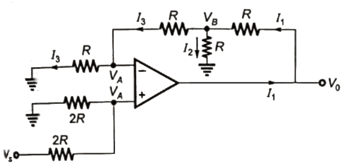
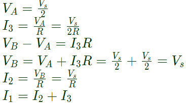
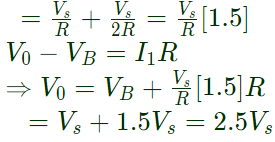
Q11: The approximate transfer characteristic for the circuit shown below with an ideal operational amplifier and diode will be (SET-1 (2017))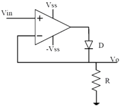 (a)
(a) 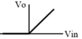 (b)
(b) 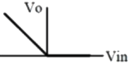 (c)
(c) 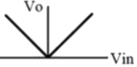 (d)
(d) 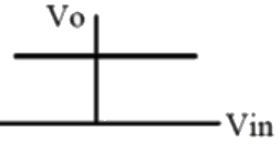 Ans: (a)
Sol: 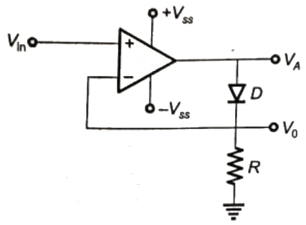 Vin > 0 VA = +V55, D on, Vo = Vin
Vin < 0 VA = −V55, D off, Vo = 0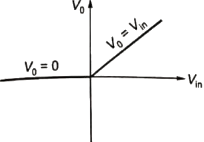
Q12: For the circuit shown below, taking the opamp as ideal, the output voltage Vout in terms of the input voltages V1, V2 and V3 is (SET-2(2016))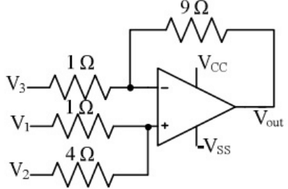 (a) 1.8V1 + 7.2V2 − V3
(b) 2V1 + 8V2 − 9V3
(c) 7.2V1 + 1.8V2 − V3
(d) 8V1 + 2V2 − 9V3
Ans: (d)
Sol: 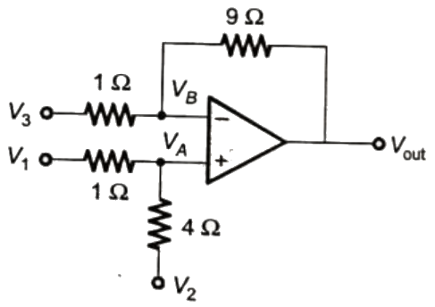
 Vout = −9V3 + 10VA
= −9V3 + 8V1 + 2V2
Q13: The circuit shown below is an example of a (SET-2(2016))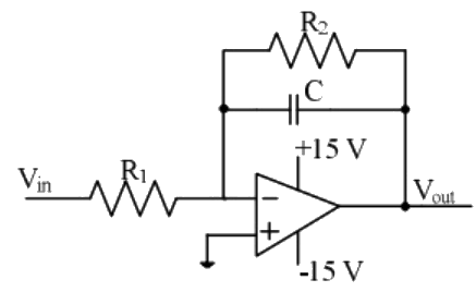 (a) low pass filter.
(b) band pass filter
(c) high pass filter.
(d) notch filter.
Ans: (a)
Sol: 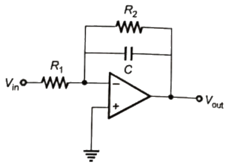
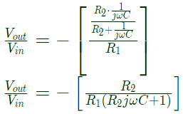 So the system is a low pass filter.
Q14: The saturation voltage of the ideal op-amp shown below is ±10 V. The output voltage v0 of the following circuit in the steady-state is (SET-2 (2015))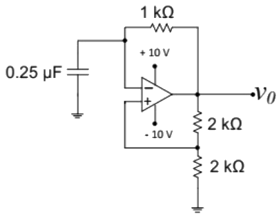 (a) square wave of period 0.55 ms.
(b) triangular wave of period 0.55 ms
(c) square wave of period 0.25 ms.
(d) triangular wave of period 0.25 ms.
Ans: (a)
Sol: The given circuit in a astable multivibrator, so output will be a periodic square wave and from the circuit β = 0.5.
So, time period will be 2τ ln (1+β)/(1−β)
Q15: The filters F1 and F2 having characteristics as shown in Figures (a) and (b) are connected as shown in Figure (c).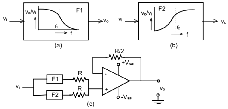 The cut-off frequencies of F1 and F2 are f1 and f2 respectively. If f1 < f2 , the resultant circuit exhibits the characteristic of a (SET-2(2015))
(a) Band-pass filter
(b) Band-stop filter
(c) All pass filter
(d) High-Q filter
Ans: (b)
Sol: To check the type of system:
we apply a delta function at input Vi = δ(t)
V(f) = 1∀f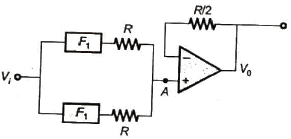 So, voltage at A will be same as voltage at output Vo. VA will be equal to voltage due to F1+ voltage due to F2. Since, f1 < f2, so VA/Vi will be
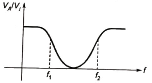
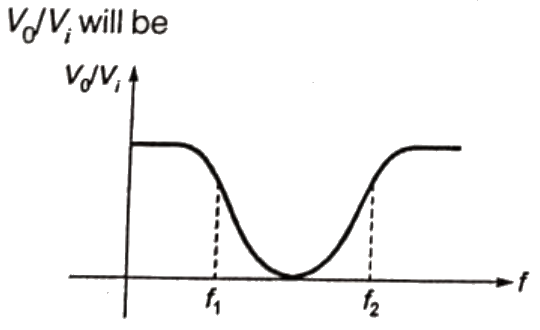 so, the system works as a band stop filter.
|
137 videos|143 docs|71 tests
|
FAQs on Previous Year Questions- Operational Amplifiers - 1 - Analog and Digital Electronics - Electrical Engineering (EE)

|
Explore Courses for Electrical Engineering (EE) exam
|

|


