Q1: Consider 4-variable functions f1, f2, f3, f4 expressed in sum-of-minterms form as given below.
f1 = ∑(0, 2, 3, 5, 7, 8, 11, 13)
f2 = ∑(1, 3, 5, 7, 11, 13, 15)
f3 = ∑(0, 1, 4, 11)
f4 = ∑(0, 2, 6,13)
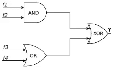 With respect to the circuit given above, which of the following options is/are CORRECT? (2014 SET-2)
(a) Y = ∑(0, 1, 2, 11, 13)
(b) Y = I(3, 4, 5, 6, 7, 8, 9, 10, 12, 14, 15)
(c) Y = ∑(0, 1, 2, 3, 4, 5, 6, 7)
(d) Y = II(8, 9, 10, 11, 12, 13, 14, 15)
Ans: (c, d)
Sol:
Here and gate is performed as intersection operations as it will return common elements between f1, f2
or gate is performed as a union operation as it will return all the elements present in both f3, f4
Assume the output of the AND gate is y₁ and the output of the OR gate is y2.
Y1 = f1 . f2 = ∑m (3, 5, 7, 11, 13)
Y2 = f3 + f4 = ∑m (0, 1, 2, 4, 6, 11, 13)
Now both Y1, Y2 act as input for XOR gate which returns the elements that is in either in
Y1 or in Y2. It will discard the common elements between Y1, Y2.
So the output
Y = Y1 ⊕ Y2 = ∑m (0, 1, 2, 3, 4, 5, 6, 7) = IIm (8, 9, 10, 11, 12, 13, 14, 15)
So Option (C, D) is correct.
Q2: Consider the circuit shown below where the gates may have propagation delays. Assume that all signal transitions occur instantaneously and that wires have no delays. Which of the following statements about the circuit is/are CORRECT? (2024 SET-1)
 (a) With no propagation delays, the output Y is always logic Zero
(b) B With no propagation delays, the output Y is always logic One
(c) With propagation delays, the output Y can have a transient logic One after X transitions from logic Zero to logic One
(d) With propagation delays, the output Y can have a transient logic Zero after X transitions from logic One to logic Zero
Ans: (a, c)
Sol:
Case 1: when there is no propagation delay, this circuit is a simple combinational circuit XX' which is always false or Logic 0.
Case 2: If we consider the delay in the Not gate, When the signal X transitions from 0 to 1, And if the delay of the And gate is larger than the not gate momentarily the Not gate will be outputing the older (incorrect) signal, because of this we will have a transient (also called temporary) logical 1 output from the circuit.
Q3: A Boolean digital circuit is composed using two 4-input multiplexers (M1 and M2) and one 2-input multiplexer (M3) as shown in the figure. X0-X7 are the inputs of the multiplexers M1 and M2 and could be connected to either 0 or 1. The select lines of the multiplexers are connected to Boolean variables A, B and C as shown. (2023)
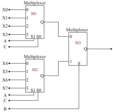 Which one of the following set of values of (X0, X1, X2, X3, X4, X5, X6, X7) will realise the Boolean function
 ?
?
(a) (1, 1, 0, 0, 1, 1, 1, 0)
(b) (1, 1, 0, 0, 1, 1, 0, 1)
(c) (1, 1, 0, 1, 1, 1, 0, 0)
(d) (0, 0, 1, 1, 0, 1, 1, 1)
Ans: (c)
Sol:

Since, final output is given by a 2 x1 MUX i.e. M3, so we have to write f as
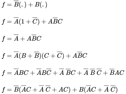
Now, our job is completed to write f as f =
Now, for
we have to go upper left side MUX i.e. M1 and we get:
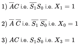
Now, from left below MUX i.e. M2, we get:

Hence, X0 = X1= X3 = X4 = X5 = 1 and X2 = X6 = X7 = 0
So, order is: 11011100
Therefore, (C)
Q4: The output of a 2-input multiplexer is connected back to one of its inputs as shown in the figure.
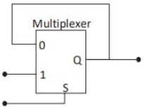 Match the functional equivalence of this circuit to one of the following options. (2023)
(a) D Flip-flop
(b) D Latch
(c) Half-adder
(d) Demultiplexer
Ans: (b)
Sol:
Here, input "0" is considered as I0 and input "1" is considered as I1 and output Q is considered as Y for the given MUX.
As we can see in the given figure that I0 = Y, I0 is storing the previous state of output Y.
Now, the basic function of D Latch is:
1) When Enable(E) = 0, Output state has the same its previous state, we call it as Memory State or you can say informally as Qn+1 = Qn
2) When Enable(E) = 1, Output variable = Input variable
Now, here, make the setting as:
Input: I1 and Enable(E)= S
Now, As we have already seen that I0 is storing the previous state of output. So, Say, previous state of output is Yold and Next state of output is Ynew
Now, According to the equation of 2 x 1 MUX i.e.
Since, I0 = Yold
Hence, we have

Now,
1) Make Enable(E)= S = 0, we get,
Ynew = Yold (i.e. Memory State for the D Latch)
2) Make Enable(E) = S = 1, we get,
Ynew = I1 (i.e. output = input)
Hence, given circuit is equivalent to D Latch.
Therefore, (B)
Q5: Which one of the following circuits implements the Boolean function given below? (2021-SET-2)
f(x, y, z) = m0 + m1 + m3 + m4 + m5 +m6
where mi is the ith minterm.
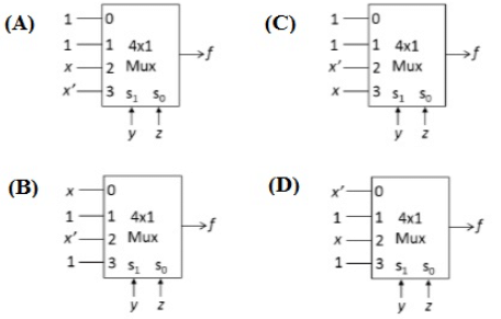
(a) A
(b) B
(c) C
(d) D
Ans: (a)
Sol:
- f(x, y, z) = m0 + m1 + m3 + m4 + m5 + m6
- S1 = y, S0 = z
Draw a small table as following and mark the min-terms in f.


A is Correct.
Q6: If there are m input lines and n output lines for a decoder that is used to uniquely address a byte addressable 1 KB RAM, then the minimum value of m + n is ________ . (2020)
(a) 20
(b) 2048
(c) 1034
(d) 1024
Ans: (c)
Sol:
Given that we need to address every byte of a 1 KB RAM.
Therefore 1K addresses are needed.
By using decoder, output lines should be n = 1 K = 1024.
This means we should have number of input lines, m = log2 1024 = 10.
Thus, m + n = 10 + 1024 = 1034.
Q7: A multiplexer is placed between a group of 32 registers and an accumulator to regulate data movement such that at any given point in time the content of only one register will move to the accumulator. The number of select lines needed for the multiplexer is ______. (2020)
(a) 8
(b) 32
(c) 5
(d) 6
Ans: (c)
Sol:
If there are ‘m ’ select lines for a multiplexer, then it may have up to 2m input lines.
Given that there are 32 input lines. So, there must be [log2 n] = [log2 32] = 5 select lines.
Q8: When two 8-bit numbers A7. . . . A0 and B7. . . . B0 in 2's complement representation (with A0 and B0 as the least significant bits) are added using a ripple-carry Combinational Circuit, the sum bits obtained are S7. . . . S0 and the carry bits are C7. . . . C0 An overflow is said to have occurred if (2017 SET-1)
(a) the carry bit C7 is 1
(b) all the carry bits (C7 . . . . C0) are 1
(c)
(d)
Ans: (c)
Sol:
Overflow is said to occur in the following cases
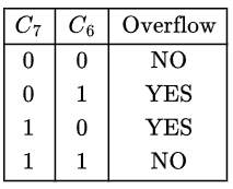
The 3rd condition occurs in the following case A7 B7S'7, now the question arises how?
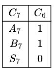
NOW, A7 = 1 AND B7 = 1, S7 = 0 is only possible when C6 = 0 otherwise S7 would become 1.
C7 has to be 1(1 + 1 + 0 generates carry)
ON similar basis we can prove that C7 = 0 and C6 = 1 is produced by A'7 B'7 S'7.
Hence, either of the two conditions cause overflow. Hence (C).
Why not A? when C7 = 1 and C6 = 1 this doesn't indicate overflow (4th row in the table)
Why not B? if all carry bits are 1 then, C7 = 1 and C6 = 1 (This also generates 4th row)
Why not D? These combinations are C0 and C1, the lower carrys do not indicate overflow
Q9: Consider an eight-bit ripple-carry Combinational Circuit for computing the sum of A and B, where A and B are integers represented in 2's complement form. If the decimal value of A is one, the decimal value of B that leads to the longest latency for the sum to stabilize is ______. (2016 SET-2)
(a) 0
(b) 1
(c) -1
(d) 2
Ans: (c)
Sol:
In ripple-carry adder, the carry "ripples" from one bit to the next. The longest path delay through n-bit ripple carry adder is 2n gate delays.
For this condition (longest latency) to arise, we must ensure that a carry that is generated at the least significant bit is propagated throughout till the last bit. This means we must have Cin = 1 for every stage of the ripple-carry adder.
Given A = +1 (in 2's complement form), we just need to find what should be B in 2's complement form to satisfy the given condition.
A = 0000 0001 (given)
B = 1111 1111 (-1 in decimal)
On adding A+B we get Cin = 1 at every stage with the last Cout = 1.
∴ Ans is -1.
Q10: Consider the two cascaded 2-to-1 multiplexers as shown in the figure. (2016 SET-1)
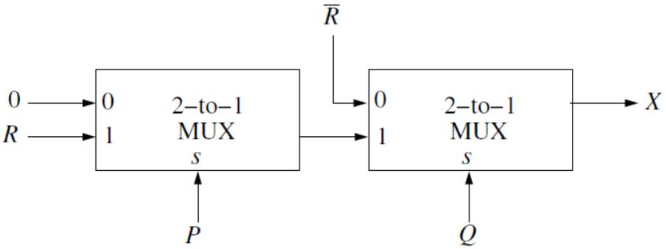 The minimal sum of products form of the output X is
(a)
(b)
(c)
(d)
Ans: (d)
Sol:
For 2: 1 MUX, output Y = S'I0. + SI1
So, output of MUX1, f1 = P'0 + PR = PR
Output of MUX2, f2 = Q'R' + Qf1 = Q'R' + PQR
which is option D
Q11: A half Combinational Circuit is implemented with XOR and AND gates. A full Combinational Circuit is implemented with two half Combinational Circuits and one OR gate. The propagation delay of an XOR gate is twice that of an AND/OR gate. The propagation delay of an AND/OR gate is 1.2 microseconds. A 4-bit ripple-carry binary Combinational Circuit is implemented by using four full Combinational Circuits. The total propagation time of this 4-bit binary Combinational Circuit in microseconds is _________. (2015 SET-2)
(a) 4.8
(b) 14.4
(c) 19.2
(d) 21.3
Ans: (c)
Sol:
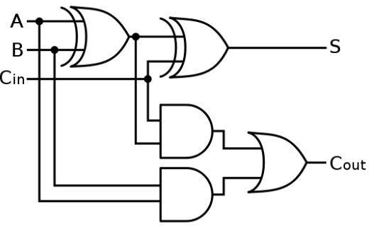 S1 should wait for C1 to be ready. Delay for generating C is 1 EXOR +1 AND +1 OR
2.4 + 1.2 + 1.2 = 4.8 μs
Delay for sum is XOR + XOR = 2.4 + 2.4 = 4.8 μs
But for the second adder, there the first EXOR can be done even before waiting for the
previous output. So, we can get the sum in Another 2.4 µs and carry in another 2.4 µs. In this
way, 4-bit sum can be obtained after
4.8 μs + 3 * 2.4 μs = 12 μs.
But the question says we use ripple-carry adder. So, each adder must wait for the full output
from the previous adder. This would make the total delay = 4 * 4.8 = 19.2 μs and this is the
key given by GATE, so obviously they meant this.
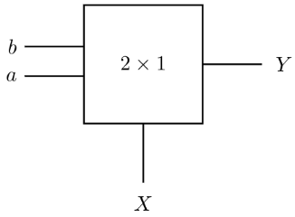
Q12: Consider the following combinational function block involving four Boolean variables x, y, a, b where x, a, b are inputs and y is the output.
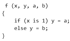
Which one of the following digital logic blocks is the most suitable for implementing this function? (2024 SET-3)
(a) Full adder
(b) Priority encoder
(c) Multiplexor
(d) Flip-flop
Ans: (c)
Sol:
If X = 1 Y = a;
else (X = 0) Y = b;
Input: (a, b, X)
Output: Y

Correct Answer: C
Q13: Consider the 4-to-1 multiplexer with two lines S1 and S0 given below. (2014 SET-1)
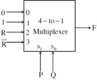 The minimal sum of-products form of the Boolean expression for the output F of the multiplexer is
(a) 
(b) 
(c)
(d)
Ans: (a)
Sol:
S1 and S0 are used to select the input given to be given as output.
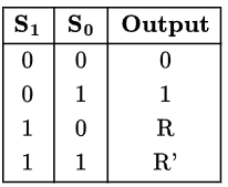
So, output becomes 1 for
S'1 S0 + S1 S'0R + S1 S0R'
= P'Q + PQ'R + PQR'
= P'Q + PQR' + PQ'
= Q(P' + PR') + PQ'R
= Q(P'+ R') + PQ'R (∵ A + A'B = A + B)
= P'Q + QR' + PQ'R
Option (A)
Q14: In the following truth table, V = 1 if and only if the input is valid.
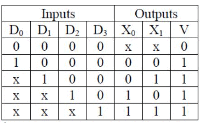 What function does the truth table represent? (2013)
(a) Priority encoder
(b) Decoder
(c) Multiplexer
(d) Demultiplexer
Ans: (a)
Sol:
Here it is a priority encoder as input bits are 2n and output bits are n also priority is defined as D3 > D2 > D1 > D0
i.e. when D3 =1 output is 01 we don't care about others, as others have less priority than D3
similarly for other if D3 = 0 D2 = 1 output is 10 we don't care about others and so on
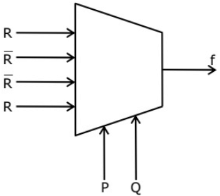
Q15: The Boolean expression for the output f of the multiplexer shown below is (2010)
 (a)
(a)
(b) P ⊕ Q ⊕ R
(c) P + Q + R
(d)
Ans: (b)
Sol:
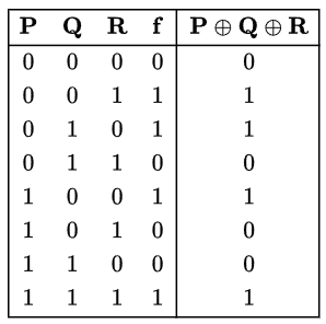
f = S'0 S'1 R + S'0 S1R' + S0S'1R' + S0S1R
= Q'P'R + Q'PR' + QP'R' + QPR
= Q'(P ⊕ R) + Q(P ⊕ R)
=Q ⊕ P ⊕ R=P ⊕ Q ⊕ R
Doing truth value substitution,

Correct Answer: B
 With respect to the circuit given above, which of the following options is/are CORRECT? (2014 SET-2)
 (a) With no propagation delays, the output Y is always logic Zero
 Which one of the following set of values of (X0, X1, X2, X3, X4, X5, X6, X7) will realise the Boolean function
 ?
?


 Match the functional equivalence of this circuit to one of the following options. (2023)


 The minimal sum of products form of the output X is


 S1 should wait for C1 to be ready. Delay for generating C is 1 EXOR +1 AND +1 OR


 The minimal sum of-products form of the Boolean expression for the output F of the multiplexer is


 What function does the truth table represent? (2013)
 (a)
(a)

