Amplifiers

Amplifier Fundamentals
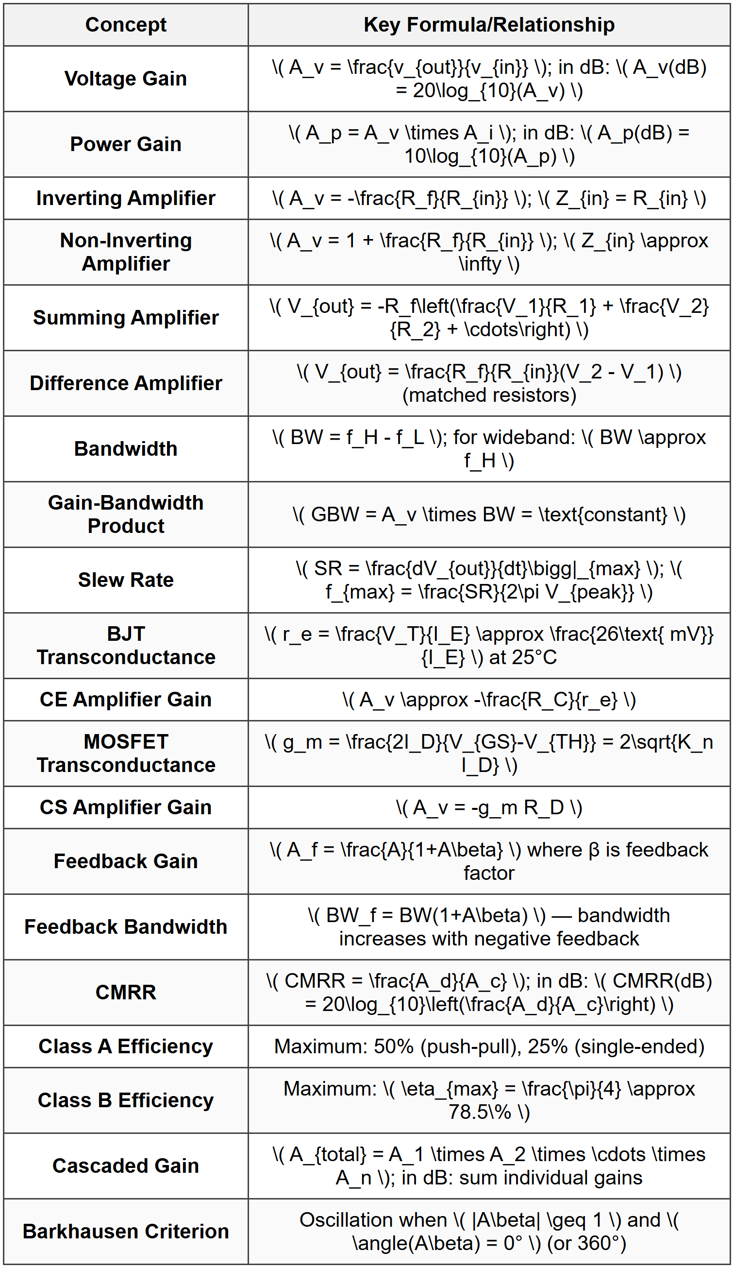
An amplifier is an electronic circuit that increases the magnitude of an input signal, producing an output signal with greater amplitude while maintaining the waveform shape. The fundamental relationship is: \[ v_{out} = A_v \cdot v_{in} \] where \( A_v \) is the voltage gain. Key Amplifier Parameters:- Voltage Gain (Av): Ratio of output voltage to input voltage, \( A_v = v_{out}/v_{in} \)
- Current Gain (Ai): Ratio of output current to input current, \( A_i = i_{out}/i_{in} \)
- Power Gain (Ap): Ratio of output power to input power, \( A_p = P_{out}/P_{in} = A_v \times A_i \)
- Input Impedance (Zin): Impedance seen by the source driving the amplifier
- Output Impedance (Zout): Impedance seen looking back into the amplifier output terminals
Operational Amplifier (Op-Amp)
The operational amplifier is a high-gain differential voltage amplifier with very high input impedance and low output impedance. An ideal op-amp exhibits:- Infinite open-loop gain (AOL → ∞)
- Infinite input impedance (Zin → ∞)
- Zero output impedance (Zout = 0)
- Infinite bandwidth
- Zero offset voltage
- No current flows into the input terminals (i+ = i- = 0)
- The voltage difference between inputs is zero (V+ = V-)
Common Op-Amp Configurations
Inverting Amplifier: \[ A_v = -\frac{R_f}{R_{in}} \] \[ Z_{in} = R_{in} \] Non-Inverting Amplifier: \[ A_v = 1 + \frac{R_f}{R_{in}} \] \[ Z_{in} \approx \infty \text{ (very high)} \] Voltage Follower (Buffer): \[ A_v = 1 \] \[ Z_{in} \approx \infty, \quad Z_{out} \approx 0 \] Summing Amplifier: \[ V_{out} = -R_f \left(\frac{V_1}{R_1} + \frac{V_2}{R_2} + \frac{V_3}{R_3}\right) \] Difference Amplifier: \[ V_{out} = \frac{R_f}{R_{in}}(V_2 - V_1) \] (when resistor ratios are matched: \( R_f/R_{in} = R_4/R_3 \))Frequency Response and Bandwidth
The bandwidth of an amplifier is the range of frequencies over which the gain remains relatively constant (typically within 3 dB of the midband gain). Lower Cutoff Frequency (fL): Frequency at which gain drops to 0.707 (-3 dB) of midband gain due to coupling and bypass capacitors. Upper Cutoff Frequency (fH): Frequency at which gain drops to 0.707 (-3 dB) of midband gain due to transistor internal capacitances. \[ BW = f_H - f_L \] For wideband amplifiers where \( f_H \gg f_L \): \[ BW \approx f_H \] Gain-Bandwidth Product (GBW): For op-amps, the gain-bandwidth product remains constant: \[ GBW = A_v \times BW = \text{constant} \] Slew Rate (SR): Maximum rate of change of output voltage: \[ SR = \frac{dV_{out}}{dt}\bigg|_{max} \text{ (V/μs)} \] The maximum frequency for undistorted sinusoidal output: \[ f_{max} = \frac{SR}{2\pi V_{peak}} \]Transistor Amplifier Configurations
Bipolar Junction Transistor (BJT) Amplifiers
Common-Emitter (CE) Configuration:- Provides voltage and current gain
- 180° phase shift between input and output
- Moderate input impedance, moderate output impedance
- Voltage gain: \( A_v \approx -\frac{R_C}{r_e} \) where \( r_e = \frac{V_T}{I_E} \approx \frac{26\text{ mV}}{I_E} \) at room temperature
- Voltage gain approximately unity (\( A_v \approx 1 \))
- High current gain
- High input impedance, low output impedance
- No phase shift
- Used for impedance matching and buffering
- Voltage gain but no current gain
- Low input impedance, high output impedance
- No phase shift
- Good high-frequency response
Field-Effect Transistor (FET) Amplifiers
For MOSFET and JFET amplifiers: Transconductance (gm): \[ g_m = \frac{\partial I_D}{\partial V_{GS}} \] For MOSFET in saturation: \[ g_m = 2\sqrt{K_n I_D} = \frac{2I_D}{V_{GS} - V_{TH}} \] Common-Source (CS) Amplifier: \[ A_v = -g_m R_D \] Common-Drain (CD) Amplifier (Source Follower): \[ A_v = \frac{g_m R_S}{1 + g_m R_S} \approx 1 \]Biasing Techniques
Proper biasing establishes the DC operating point (Q-point) to ensure linear operation and prevent distortion. Voltage Divider Bias (most stable for BJT): Q-point parameters: \[ V_B = V_{CC} \cdot \frac{R_2}{R_1 + R_2} \] \[ V_E = V_B - V_{BE} \] \[ I_E = \frac{V_E}{R_E} \] \[ I_C \approx I_E \] \[ V_{CE} = V_{CC} - I_C(R_C + R_E) \] For stability, design guideline: \( R_{TH} = R_1 \parallel R_2 \leq 0.1\beta R_E \)Feedback in Amplifiers
Negative feedback improves amplifier performance by returning a portion of the output signal to the input in opposition to the input signal. Closed-loop gain with feedback: \[ A_f = \frac{A}{1 + A\beta} \] where:- \( A \) = open-loop gain
- \( \beta \) = feedback factor
- \( A\beta \) = loop gain
- Stabilizes gain
- Increases bandwidth: \( BW_f = BW(1 + A\beta) \)
- Reduces distortion
- Controls input and output impedances
- Reduces sensitivity to component variations
- Voltage-series (non-inverting): Increases input impedance, decreases output impedance
- Voltage-shunt (inverting): Decreases both input and output impedances
- Current-series: Increases both input and output impedances
- Current-shunt: Decreases input impedance, increases output impedance
Differential Amplifier
A differential amplifier amplifies the difference between two input signals while rejecting signals common to both inputs. \[ V_{out} = A_d(V_1 - V_2) + A_c\left(\frac{V_1 + V_2}{2}\right) \] where:- \( A_d \) = differential-mode gain
- \( A_c \) = common-mode gain
Power Amplifiers
Classes of Power Amplifiers: Class A:- Transistor conducts for entire 360° cycle
- Low distortion, linear operation
- Maximum theoretical efficiency: 50% (25% for single-ended)
- High power dissipation
- Transistor conducts for 180° of cycle (push-pull configuration)
- Maximum theoretical efficiency: 78.5%
- Crossover distortion present
- Transistor conducts for slightly more than 180°
- Reduces crossover distortion of Class B
- Efficiency between Class A and Class B (50%-78.5%)
- Transistor conducts for less than 180°
- High efficiency (>78.5%), high distortion
- Used in RF applications with tuned circuits
Multi-Stage Amplifiers
When amplifiers are cascaded, the overall gain is the product of individual stage gains: \[ A_{total} = A_1 \times A_2 \times A_3 \times \ldots \times A_n \] In decibels: \[ A_{total}(dB) = A_1(dB) + A_2(dB) + A_3(dB) + \ldots + A_n(dB) \] Coupling Methods:- RC Coupling: Uses capacitors to block DC while passing AC; most common
- Direct Coupling: No coupling components; used in IC design
- Transformer Coupling: Provides impedance matching and isolation
Stability and Oscillation
An amplifier with feedback may become unstable and oscillate if the loop gain magnitude equals or exceeds unity at a frequency where the phase shift is 360° (or 0°). Barkhausen Criterion for Oscillation: \[ |A\beta| \geq 1 \] \[ \angle(A\beta) = 360° \text{ (or 0°)} \] Phase Margin (PM): Additional phase shift required at unity gain frequency to cause instability: \[ PM = 180° - \angle(A\beta)\big|_{|A\beta|=1} \] Typically, PM > 45° ensures stable operation. Gain Margin (GM): Amount by which gain can increase before instability: \[ GM(dB) = -20\log_{10}|A\beta|\big|_{\angle(A\beta)=180°} \] Typically, GM > 10 dB ensures stable operation. ## STANDARD CODES, STANDARDS & REFERENCES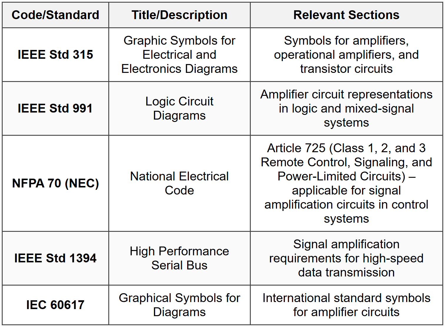 ## SOLVED EXAMPLES
Example 1: Multi-Stage Amplifier with Feedback Analysis
PROBLEM STATEMENT: A three-stage amplifier system has individual stage gains of 25, 40, and 15 respectively. A feedback network with β = 0.02 is connected around the entire amplifier system. Determine: (a) the overall open-loop gain in dB, (b) the closed-loop gain with feedback, (c) the closed-loop gain in dB, and (d) the amount of gain reduction due to feedback in dB. GIVEN DATA:- Stage 1 gain: A₁ = 25
- Stage 2 gain: A₂ = 40
- Stage 3 gain: A₃ = 15
- Feedback factor: β = 0.02
(b) Af (closed-loop gain)
(c) Af in dB
(d) Gain reduction in dB SOLUTION: Step 1: Calculate overall open-loop gain
For cascaded amplifiers, total gain is the product of individual gains:
\[ A_{OL} = A_1 \times A_2 \times A_3 \] \[ A_{OL} = 25 \times 40 \times 15 = 15,000 \] Step 2: Convert open-loop gain to dB
\[ A_{OL}(dB) = 20\log_{10}(15,000) \] \[ A_{OL}(dB) = 20 \times 4.176 = 83.52 \text{ dB} \] (a) Answer: AOL = 83.52 dB Step 3: Calculate closed-loop gain with feedback
Using the feedback formula:
\[ A_f = \frac{A_{OL}}{1 + A_{OL}\beta} \] \[ A_f = \frac{15,000}{1 + 15,000 \times 0.02} \] \[ A_f = \frac{15,000}{1 + 300} = \frac{15,000}{301} \] \[ A_f = 49.83 \] (b) Answer: Af = 49.83 Step 4: Convert closed-loop gain to dB
\[ A_f(dB) = 20\log_{10}(49.83) \] \[ A_f(dB) = 20 \times 1.698 = 33.96 \text{ dB} \] (c) Answer: Af = 33.96 dB Step 5: Calculate gain reduction due to feedback
\[ \text{Gain Reduction} = A_{OL}(dB) - A_f(dB) \] \[ \text{Gain Reduction} = 83.52 - 33.96 = 49.56 \text{ dB} \] Alternatively, the gain reduction factor equals (1 + Aβ):
\[ \text{Gain Reduction}(dB) = 20\log_{10}(1 + A_{OL}\beta) \] \[ \text{Gain Reduction}(dB) = 20\log_{10}(301) = 49.57 \text{ dB} \] (d) Answer: Gain reduction = 49.56 dB ANSWER:
(a) Open-loop gain = 83.52 dB
(b) Closed-loop gain = 49.83
(c) Closed-loop gain = 33.96 dB
(d) Gain reduction = 49.56 dB ---
Example 2: Op-Amp Summing Amplifier with Frequency Limitations
PROBLEM STATEMENT: A summing amplifier is designed using an operational amplifier with a gain-bandwidth product (GBW) of 1 MHz and a slew rate of 0.5 V/μs. The circuit has three input resistors: R₁ = 10 kΩ, R₂ = 20 kΩ, R₃ = 25 kΩ, and a feedback resistor Rf = 50 kΩ. Three input voltages are applied: V₁ = 0.5 V, V₂ = -0.3 V, and V₃ = 0.8 V. Determine: (a) the output voltage, (b) the maximum bandwidth of the amplifier, and (c) the maximum frequency at which a 2 V peak sinusoidal output can be produced without distortion. GIVEN DATA:- R₁ = 10 kΩ, R₂ = 20 kΩ, R₃ = 25 kΩ
- Rf = 50 kΩ
- V₁ = 0.5 V, V₂ = -0.3 V, V₃ = 0.8 V
- GBW = 1 MHz = 1 × 10⁶ Hz
- Slew Rate (SR) = 0.5 V/μs = 0.5 × 10⁶ V/s
- Vpeak = 2 V (for part c)
(b) Maximum bandwidth (BW)
(c) Maximum frequency for 2 V peak output (fmax) SOLUTION: Step 1: Calculate output voltage using summing amplifier formula
For a summing amplifier:
\[ V_{out} = -R_f\left(\frac{V_1}{R_1} + \frac{V_2}{R_2} + \frac{V_3}{R_3}\right) \] Substitute values:
\[ V_{out} = -50,000\left(\frac{0.5}{10,000} + \frac{-0.3}{20,000} + \frac{0.8}{25,000}\right) \] \[ V_{out} = -50,000\left(0.00005 - 0.000015 + 0.000032\right) \] \[ V_{out} = -50,000(0.000067) \] \[ V_{out} = -3.35 \text{ V} \] (a) Answer: Vout = -3.35 V Step 2: Calculate individual gains and overall closed-loop gain
For each input path, the gain magnitude is:
\[ A_{v1} = \frac{R_f}{R_1} = \frac{50,000}{10,000} = 5 \] \[ A_{v2} = \frac{R_f}{R_2} = \frac{50,000}{20,000} = 2.5 \] \[ A_{v3} = \frac{R_f}{R_3} = \frac{50,000}{25,000} = 2 \] The maximum gain determines the bandwidth. Using the highest gain path:
\[ A_{CL} = 5 \text{ (maximum closed-loop gain)} \] Step 3: Calculate maximum bandwidth using GBW
The gain-bandwidth product relationship:
\[ BW = \frac{GBW}{A_{CL}} \] \[ BW = \frac{1 \times 10^6}{5} = 200,000 \text{ Hz} = 200 \text{ kHz} \] (b) Answer: BW = 200 kHz Step 4: Calculate maximum frequency based on slew rate limitation
For a sinusoidal signal, the slew rate limitation is:
\[ SR = 2\pi f_{max} V_{peak} \] Solving for fmax:
\[ f_{max} = \frac{SR}{2\pi V_{peak}} \] \[ f_{max} = \frac{0.5 \times 10^6}{2\pi \times 2} \] \[ f_{max} = \frac{0.5 \times 10^6}{12.566} \] \[ f_{max} = 39,789 \text{ Hz} \approx 39.8 \text{ kHz} \] (c) Answer: fmax = 39.8 kHz Note: The slew rate limitation (39.8 kHz) is more restrictive than the bandwidth limitation (200 kHz) for this output amplitude, so distortion will occur above 39.8 kHz. ANSWER:
(a) Output voltage = -3.35 V
(b) Maximum bandwidth = 200 kHz
(c) Maximum frequency for 2 V peak = 39.8 kHz ## QUICK SUMMARY
 Key Terms to Remember:
- Ideal Op-Amp Golden Rules: No input current; V+ = V- (with negative feedback)
- Phase Margin: Stability measure; typically PM > 45° for stable operation
- Gain Margin: Stability measure; typically GM > 10 dB for stable operation
- 3-dB Frequency: Frequency where gain drops to 0.707 of midband value
- Voltage Divider Bias Stability Condition: \( R_{TH} \leq 0.1\beta R_E \)
- Emitter Follower: Unity gain, high input impedance, low output impedance
- Source Follower: FET equivalent of emitter follower
Question 1: A two-stage amplifier consists of a common-emitter stage with a voltage gain of 45 followed by an emitter follower with a voltage gain of 0.95. If the input signal is 20 mV RMS, what is the output voltage?
(A) 0.72 V(B) 0.86 V
(C) 0.95 V
(D) 1.14 V Correct Answer: (B) Explanation:
For cascaded amplifiers, the overall gain is the product of individual stage gains:
\[ A_{total} = A_1 \times A_2 = 45 \times 0.95 = 42.75 \] Output voltage:
\[ V_{out} = A_{total} \times V_{in} = 42.75 \times 20 \text{ mV} \] \[ V_{out} = 42.75 \times 0.020 = 0.855 \text{ V} \approx 0.86 \text{ V} \] The correct answer is (B) 0.86 V. ─────────────────────────────────────────
Question 2: Which of the following statements about operational amplifier characteristics is FALSE?
(A) Negative feedback reduces the closed-loop gain compared to open-loop gain(B) The gain-bandwidth product remains constant for a given op-amp regardless of closed-loop gain configuration
(C) Slew rate limits the maximum frequency at which large amplitude signals can be faithfully reproduced
(D) Negative feedback decreases the bandwidth of the amplifier Correct Answer: (D) Explanation:
Statement (A) is TRUE: Negative feedback reduces gain according to \( A_f = \frac{A}{1+A\beta} \), which is always less than open-loop gain A when Aβ > 0. Statement (B) is TRUE: The gain-bandwidth product (GBW) is a characteristic constant of the op-amp, and \( GBW = A_v \times BW \) remains constant. Statement (C) is TRUE: Slew rate limits the maximum rate of change of output voltage, which restricts high-frequency, large-amplitude signals according to \( f_{max} = \frac{SR}{2\pi V_{peak}} \). Statement (D) is FALSE: Negative feedback actually INCREASES bandwidth according to \( BW_f = BW(1+A\beta) \). This is one of the key benefits of negative feedback-reduced gain is traded for increased bandwidth through the gain-bandwidth product relationship. The correct answer is (D). ─────────────────────────────────────────
Question 3: An industrial control system requires an amplifier to process signals from three temperature sensors. The sensor outputs are 150 mV, 220 mV, and 180 mV respectively. An engineer designs a summing amplifier circuit to combine these signals with equal weighting and produce an output that is the negative average of the inputs multiplied by 10. If all input resistors are 15 kΩ, what value of feedback resistor should be used?
(A) 45 kΩ(B) 50 kΩ
(C) 150 kΩ
(D) 450 kΩ Correct Answer: (B) Explanation:
For a summing amplifier with equal input resistors:
\[ V_{out} = -R_f\left(\frac{V_1}{R_1} + \frac{V_2}{R_2} + \frac{V_3}{R_3}\right) \] With R₁ = R₂ = R₃ = R:
\[ V_{out} = -\frac{R_f}{R}(V_1 + V_2 + V_3) \] The requirement is to produce the negative average multiplied by 10:
\[ V_{out} = -10 \times \frac{V_1 + V_2 + V_3}{3} \] Comparing the two expressions:
\[ -\frac{R_f}{R}(V_1 + V_2 + V_3) = -10 \times \frac{V_1 + V_2 + V_3}{3} \] \[ \frac{R_f}{R} = \frac{10}{3} \] \[ R_f = \frac{10R}{3} = \frac{10 \times 15,000}{3} = \frac{150,000}{3} = 50,000 \text{ Ω} = 50 \text{ kΩ} \] The correct answer is (B) 50 kΩ. ─────────────────────────────────────────
Question 4: According to NEC Article 725, which classification would typically apply to low-voltage control circuits containing signal amplifiers operating at 24 VDC with a maximum current-limited power supply of 100 VA?
(A) Class 1 Remote Control Circuit(B) Class 2 Power-Limited Circuit
(C) Class 3 Power-Limited Circuit
(D) Not covered under Article 725 Correct Answer: (B) Explanation:
NEC Article 725 classifies remote control, signaling, and power-limited circuits. The classification depends on voltage and power levels: Class 1 Circuits: Not inherently power-limited; can operate at higher voltages and power levels but must comply with general wiring methods. Class 2 Circuits: Power-limited to levels not exceeding 100 VA (or specific current limits). For circuits operating at 20-30 VAC or 30 VDC or less, the power limit is 100 VA. The 24 VDC system with 100 VA maximum falls within Class 2 requirements. Class 3 Circuits: Power-limited but at higher levels than Class 2 (typically 100 VA to specific limits based on voltage). Given:
- Voltage: 24 VDC
- Power: 100 VA (current-limited power supply)
Question 5: A manufacturer provides the following specifications for a series of operational amplifiers being evaluated for a precision instrumentation application:

The application requires processing three input signals in a differential configuration with high common-mode noise rejection (CMRR > 95 dB) and the ability to handle a closed-loop gain of 50 at frequencies up to 30 kHz. Which op-amp should be selected?
(A) OP-101(B) OP-202
(C) OP-303
(D) OP-404 Correct Answer: (D) Explanation:
Two requirements must be satisfied: Requirement 1: CMRR > 95 dB
Examining the CMRR column:
- OP-101: 90 dB ✗ (does not meet requirement)
- OP-202: 110 dB ✓
- OP-303: 80 dB ✗ (does not meet requirement)
- OP-404: 100 dB ✓
Using the gain-bandwidth relationship:
\[ BW = \frac{GBW}{A_{CL}} \] For OP-202:
\[ BW = \frac{0.5 \times 10^6}{50} = 10,000 \text{ Hz} = 10 \text{ kHz} \] This is less than 30 kHz required ✗ For OP-404:
\[ BW = \frac{2.0 \times 10^6}{50} = 40,000 \text{ Hz} = 40 \text{ kHz} \] This exceeds 30 kHz required ✓ Only OP-404 meets both requirements. The correct answer is (D) OP-404. ─────────────────────────────────────────