PE Exam Exam > PE Exam Notes > Electrical & Computer Engineering for PE > Cheatsheet: Amplifiers
Cheatsheet: Amplifiers


1. Amplifier Fundamentals
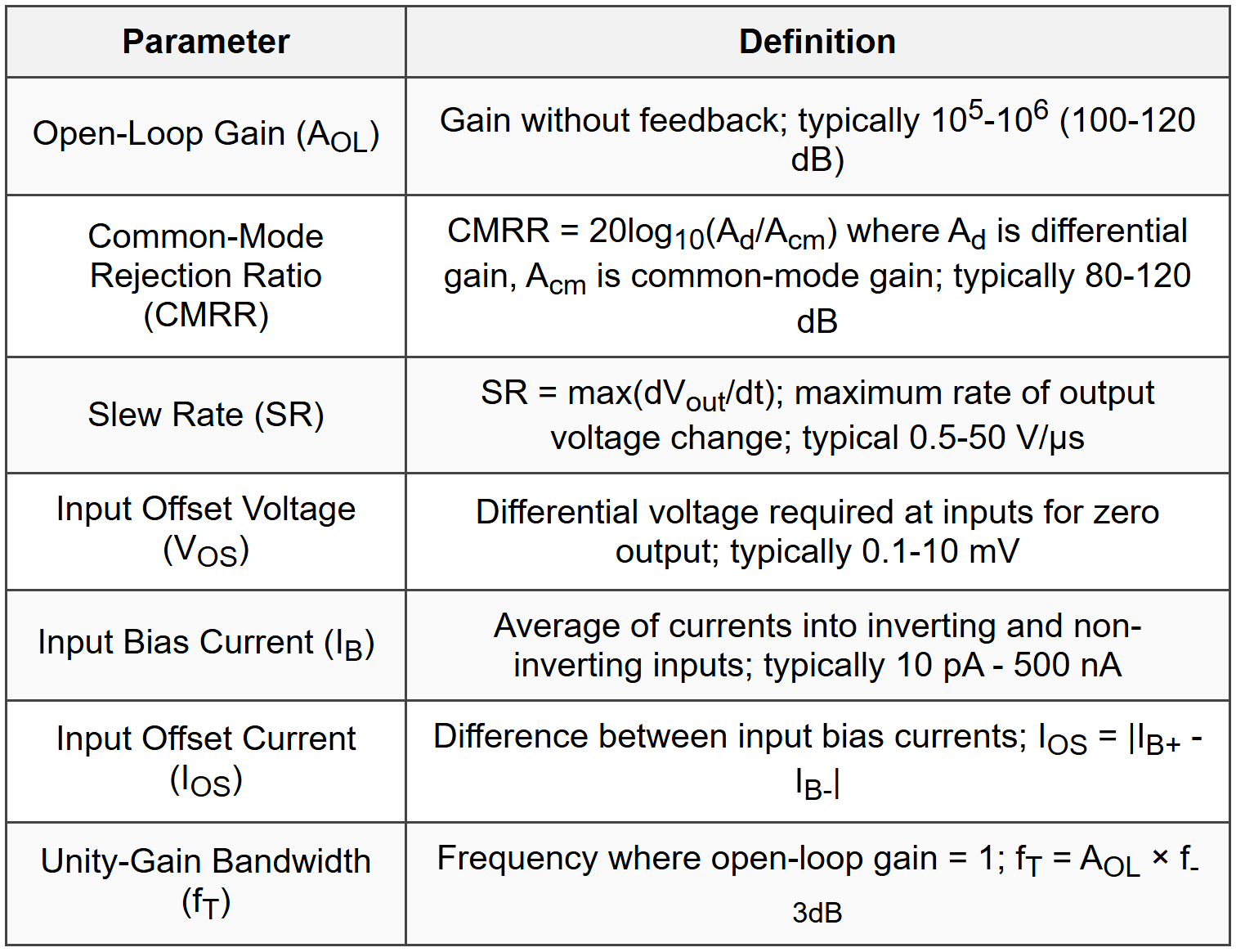
1.1 Key Parameters

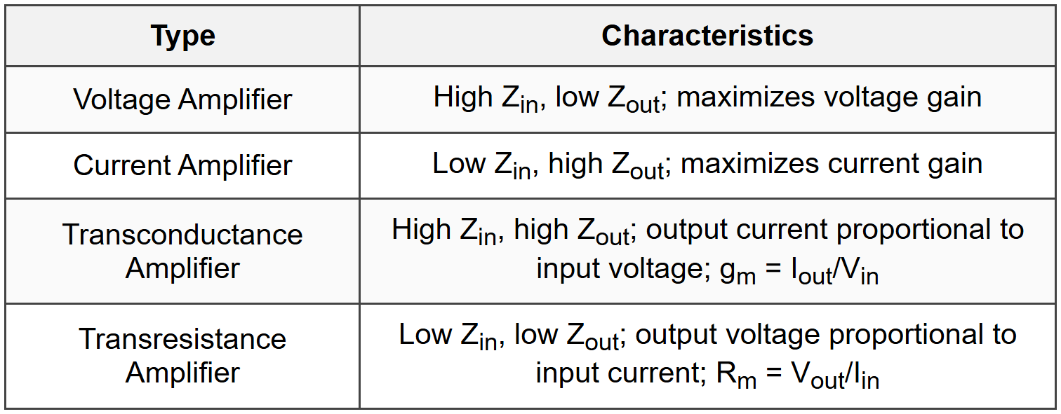
1.2 Amplifier Classifications
2. BJT Amplifier Configurations
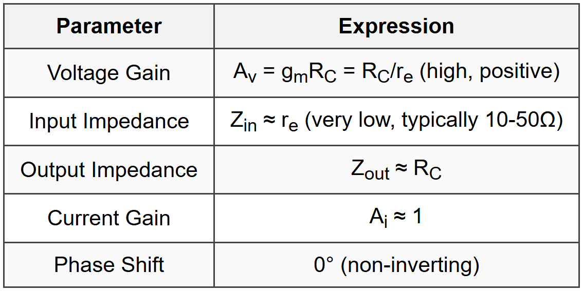
2.1 Common Emitter (CE)

- Most common configuration; moderate Zin, high voltage and current gain
- With emitter degeneration RE: Av = -RC/(re + RE); Zin = β(re + RE)
2.2 Common Collector (CC) / Emitter Follower
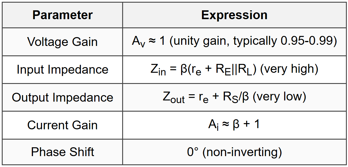
- Buffer amplifier; excellent for impedance matching
- High input impedance, low output impedance
2.3 Common Base (CB)
- High frequency response; good voltage gain, no current gain
- Very low input impedance; used in RF applications
2.4 Configuration Comparison

3. MOSFET Amplifier Configurations
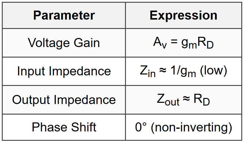
3.1 Common Source (CS)

- With source degeneration RS: Av = -gmRD/(1 + gmRS)
- Extremely high input impedance due to gate insulation
3.2 Common Drain (CD) / Source Follower

- Unity gain buffer; excellent for impedance transformation
3.3 Common Gate (CG)
- High frequency response; low input impedance
- Used in cascode configurations and RF circuits
3.4 Small-Signal Parameters

4. Operational Amplifier Fundamentals
4.1 Ideal Op-Amp Characteristics
- Infinite open-loop gain: AOL → ∞
- Infinite input impedance: Zin → ∞
- Zero output impedance: Zout = 0
- Infinite bandwidth: BW → ∞
- Zero input offset voltage: VOS = 0
- Infinite CMRR and PSRR
- Zero input bias current: IB = 0
4.2 Key Real Op-Amp Parameters
4.3 Golden Rules for Ideal Op-Amp Analysis
- Rule 1: No current flows into either input terminal (I+ = I- = 0)
- Rule 2: With negative feedback, V+ = V- (virtual short)
5. Op-Amp Circuit Configurations
5.1 Inverting Amplifier
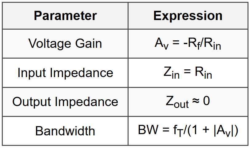
- Vout = -(Rf/Rin)Vin
- Non-inverting input grounded; signal applied to inverting input through Rin
5.2 Non-Inverting Amplifier

- Vout = (1 + Rf/Rin)Vin
- Signal applied to non-inverting input; inverting input connected to voltage divider
5.3 Voltage Follower (Unity Gain Buffer)
- Av = 1 (special case of non-inverting with Rf = 0, Rin → ∞)
- Vout = Vin
- Maximum bandwidth: BW = fT
- Very high input impedance, very low output impedance
5.4 Summing Amplifier
- Vout = -(Rf/R1)V1 - (Rf/R2)V2 - ... - (Rf/Rn)Vn
- Inverting configuration with multiple inputs
- If all Ri = R, then Vout = -(Rf/R)(V1 + V2 + ... + Vn)
5.5 Difference Amplifier (Differential)
- Vout = (Rf/Rin)(V2 - V1) when resistor ratios matched: Rf/Rin = R4/R3
- Amplifies difference between two inputs; rejects common-mode signals
- CMRR depends on resistor matching accuracy
5.6 Instrumentation Amplifier
- Three op-amp configuration: two input buffers + one difference amplifier
- Av = (1 + 2R2/Rgain)(Rf/Rin)
- Very high input impedance, high CMRR (>100 dB), adjustable gain with single resistor
- Vout = Av(V2 - V1)
5.7 Integrator
- Vout(t) = -1/(RinC) ∫Vin(t)dt + Vout(0)
- Feedback element is capacitor C
- Gain = -1/(jωRinC); magnitude decreases with frequency at -20 dB/decade
- Phase shift: -90° (plus 180° from inverting)
5.8 Differentiator
- Vout(t) = -RfC(dVin/dt)
- Input element is capacitor C
- Gain = -jωRfC; magnitude increases with frequency at +20 dB/decade
- Prone to noise amplification at high frequencies; often use series resistor with C for stability
6. Frequency Response & Bandwidth
6.1 Frequency Response Concepts
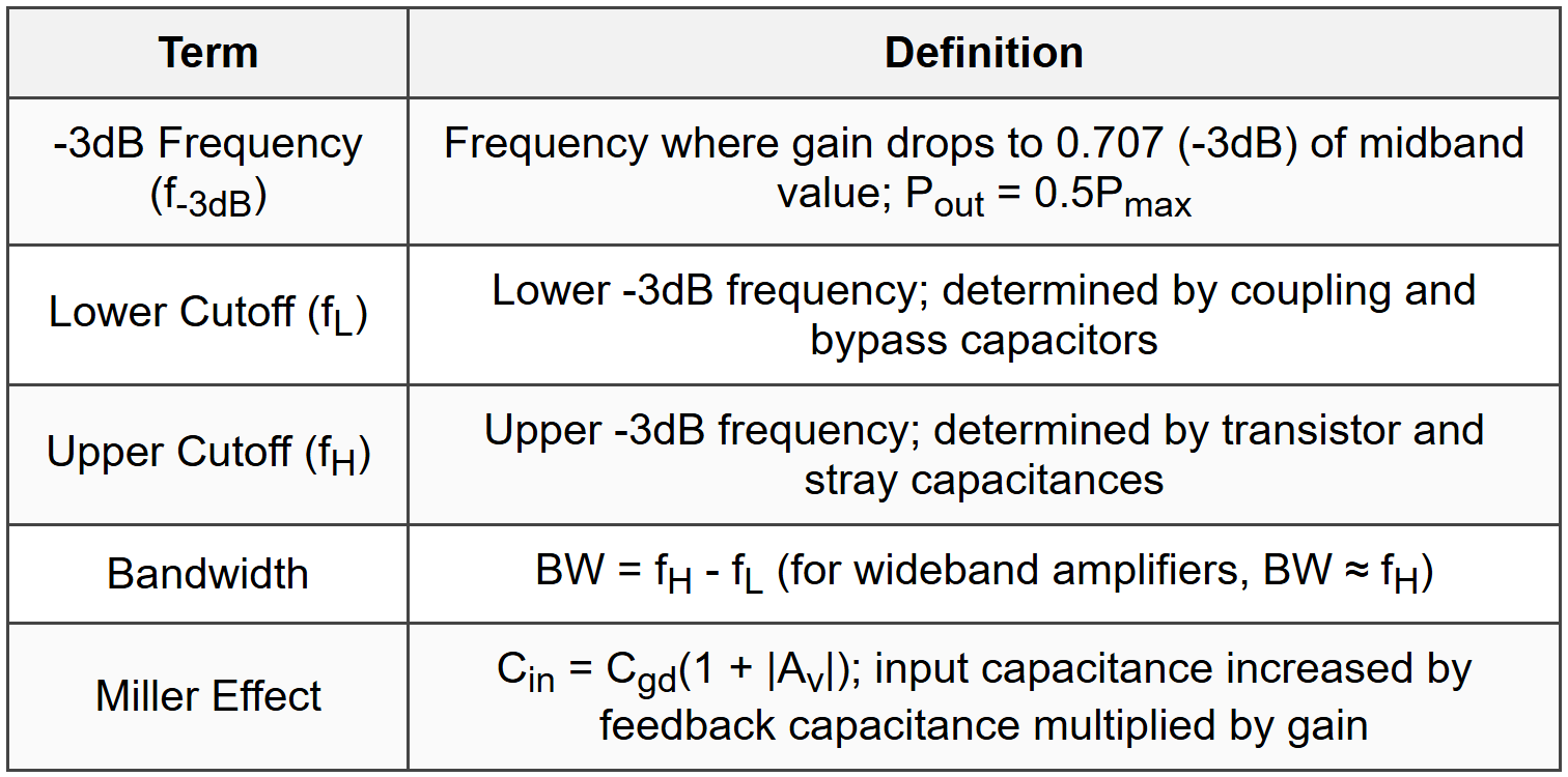
6.2 Dominant Pole Approximation
- f-3dB = 1/(2πRC) for single-pole system
- When one pole frequency much lower than others, it dominates frequency response
- Roll-off: -20 dB/decade per pole
6.3 Bode Plot Characteristics
- Single pole: -20 dB/decade slope, -90° phase shift
- Two poles: -40 dB/decade slope, -180° phase shift
- Single zero: +20 dB/decade slope, +90° phase shift
- Phase margin: 180° - |∠A(jω)| at unity gain frequency; PM > 45° for stability
- Gain margin: 1/|A(jω)| at -180° phase; GM > 1 (0 dB) for stability
6.4 Feedback Effects on Bandwidth
- Closed-loop bandwidth: BWCL = BWOL(1 + βAOL) where β is feedback factor
- Gain-bandwidth product remains constant: Av × BW = fT
- Negative feedback trades gain for bandwidth
7. Power Amplifiers
7.1 Class A Amplifier
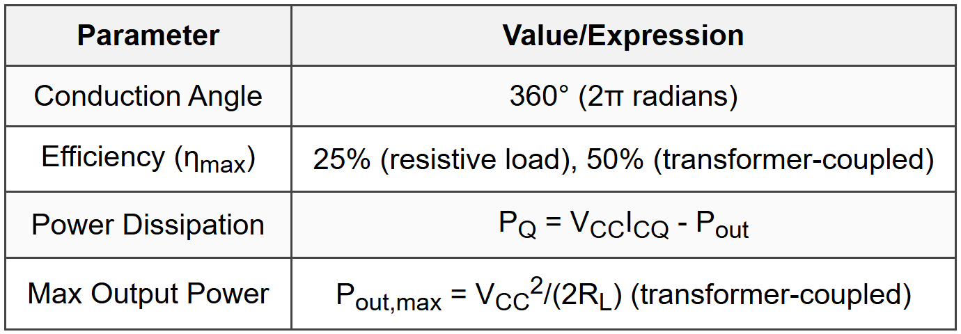
- Transistor conducts for entire input cycle
- Biased at midpoint of load line (Q-point at center)
- Low distortion, low efficiency
- Largest power dissipation at zero signal
7.2 Class B Amplifier (Push-Pull)
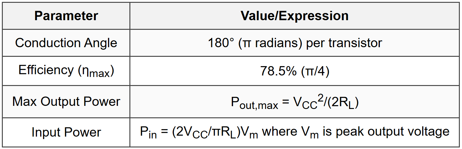
- Two transistors: one for positive half-cycle, one for negative half-cycle
- Crossover distortion at zero crossing (VBE threshold)
- Higher efficiency than Class A; zero quiescent power
- η = (π/4)(Vm/VCC) where Vm is peak output voltage
7.3 Class AB Amplifier
- Conduction angle between 180° and 360°
- Small bias current to reduce crossover distortion
- Efficiency: 50-70% (between Class A and Class B)
- Most common for audio amplifiers; compromise between efficiency and distortion
7.4 Class C Amplifier

- Transistor conducts for less than half cycle
- Requires resonant tank circuit to reconstruct waveform
- High distortion; used only for RF applications with tuned loads
- Not suitable for linear amplification
7.5 Class D Amplifier (Switching)
- Transistors operate as switches (fully on or fully off)
- Pulse-width modulation (PWM) encodes signal amplitude
- Efficiency: >90% (up to 95-98%)
- Requires output low-pass filter to reconstruct analog signal
- Minimal power dissipation in transistors
7.6 Power Amplifier Comparison

7.7 Heat Sink Design
- θJA = θJC + θCS + θSA where J=junction, C=case, S=sink, A=ambient
- Maximum junction temperature: TJ = TA + PDθJA
- Required thermal resistance: θSA = (TJ,max - TA)/PD - θJC - θCS
- Thermal resistance units: °C/W
8. Feedback Amplifiers
8.1 Feedback Fundamentals

- Negative feedback: loop gain βA is subtracted from input
- Positive feedback: loop gain βA is added to input (can cause oscillation)
8.2 Effects of Negative Feedback

8.3 Feedback Topologies

8.4 Stability and Oscillation
- Barkhausen Criterion for oscillation: |βA| = 1 and ∠(βA) = 0° (or 360°)
- Nyquist Stability Criterion: system stable if (-1, j0) point not encircled by Nyquist plot
- Phase Margin (PM): 180° + ∠(βA) at |βA| = 1; PM > 45° for adequate stability
- Gain Margin (GM): 20log10(1/|βA|) at ∠(βA) = -180°; GM > 10 dB recommended
- Compensation techniques: dominant-pole, lead, lag, lag-lead
9. Differential Amplifiers
9.1 Basic Differential Pair
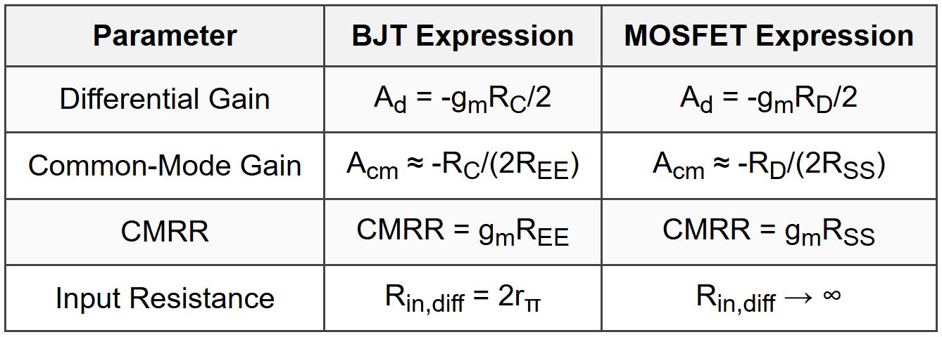
- Vout,diff = Ad(V1 - V2)
- Tail current source IEE or ISS improves CMRR
- Single-ended output: half the differential gain
9.2 Active Load Differential Amplifier
- Current mirror replaces resistive loads
- Ad = gm(ro||roc) where roc is output resistance of current mirror
- Much higher gain than resistive load (50-80 dB vs 20-40 dB)
- Better DC matching and smaller chip area
9.3 Differential Mode vs Common Mode
- Differential input: Vid = V1 - V2
- Common-mode input: Vicm = (V1 + V2)/2
- V1 = Vicm + Vid/2; V2 = Vicm - Vid/2
- Vout = AdVid + AcmVicm
10. Multistage Amplifiers
10.1 Cascaded Amplifier Gain
- Total voltage gain: Av,total = Av1 × Av2 × ... × Avn
- In dB: Av,total(dB) = Av1(dB) + Av2(dB) + ... + Avn(dB)
- Loading effects must be considered between stages
- Overall bandwidth limited by stage with smallest BW
10.2 Cascode Amplifier
- CE (or CS) stage followed by CB (or CG) stage
- Av ≈ -gm1(ro1||rin2)gm2RL ≈ -gm2roRL
- High gain, wide bandwidth, excellent isolation
- Miller effect minimized (low Cin)
- Output resistance: Rout ≈ gm2ro1ro2 (very high)
10.3 Darlington Pair
- Two BJTs in series: collector of Q1 to collector of Q2, emitter of Q1 to base of Q2
- Current gain: βtotal ≈ β1β2
- Input impedance: Zin = β1β2(re2 + RE)
- VBE,total = VBE1 + VBE2 ≈ 1.4V
- Used for very high current gain applications
10.4 Buffer Stages
- Emitter follower (BJT) or source follower (FET) provides impedance transformation
- Placed between high-Z source and low-Z load
- Prevents loading of previous stage
- Unity voltage gain, high current gain
11. Distortion and Noise
11.1 Types of Distortion

11.2 Noise Sources

11.3 Noise Figure and SNR
- Signal-to-Noise Ratio: SNR = Psignal/Pnoise or 10log10(PS/PN) dB
- Noise Figure: NF = SNRin/SNRout or NF(dB) = 10log10(SNRin/SNRout)
- Equivalent input noise: eni2 = 4kTRSΔf + en,amp2
- Cascaded noise figure: Ftotal = F1 + (F2-1)/G1 + (F3-1)/(G1G2) + ...
11.4 Dynamic Range
- Dynamic Range = 20log10(Vmax/Vmin) where Vmin limited by noise, Vmax by distortion
- Spurious-Free Dynamic Range (SFDR): ratio of fundamental to largest spurious signal
- Signal-to-Noise-and-Distortion Ratio: SINAD = Psignal/(Pnoise + Pdistortion)
12. Current Sources and Mirrors
12.1 BJT Current Mirror
- Basic mirror: Iout/Iref = 1 (assuming β >> 1)
- Actual ratio: Iout/Iref = β/(β+2) ≈ 1 - 2/β
- Output resistance: rout = ro = VA/IC
- Ratio scaling: Iout/Iref = (AE,out/AE,ref) for matched transistors
12.2 MOSFET Current Mirror
- Basic mirror: Iout/Iref = (W/L)out/(W/L)ref
- Both transistors must be in saturation: VDS ≥ VGS - Vth
- Output resistance: rout = ro = 1/(λID)
- Better matching than BJT at low currents
12.3 Improved Current Mirrors

12.4 Widlar Current Source
- VTln(Iref/Iout) = IoutRE
- Allows generation of small currents (μA) from larger reference (mA)
- Emitter resistor RE only on output transistor
13. Practical Design Considerations
13.1 Biasing Techniques
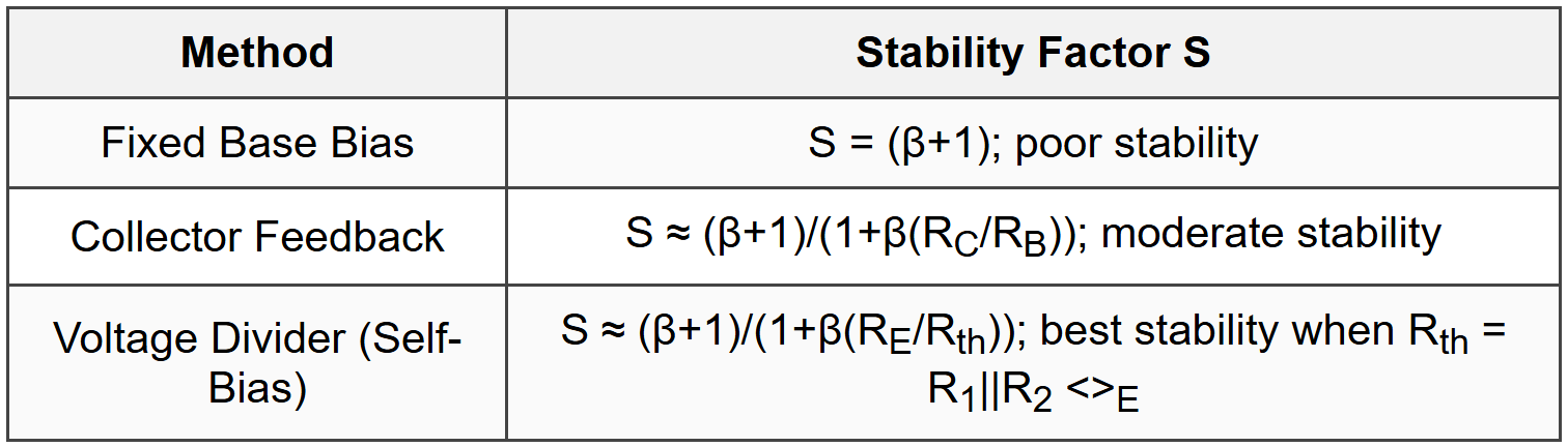
- Stability factor: S = dIC/dICO; lower is better
- Design rule: I2 ≈ 10IB where I2 is current through R2
13.2 Coupling and Bypass Capacitors
- Coupling capacitor: XC <>in at lowest frequency; C ≥ 10/(2πfLRin)
- Bypass capacitor: XC <>E at lowest frequency; typically C ≥ 10/(2πfLRE)
- Power supply decoupling: 0.1μF ceramic + 10-100μF electrolytic in parallel
13.3 Input/Output Impedance Matching
- Maximum power transfer: RL = RS (impedance matched)
- Maximum voltage transfer: RL >> RS (high Zin desired)
- Maximum current transfer: RL <>S (low Zin desired)
- Impedance transformation: n2 = Z1/Z2 for transformer with turns ratio n
13.4 Temperature Effects
- BJT: VBE decreases ~2 mV/°C; ICO doubles every 10°C
- MOSFET: Vth decreases ~2 mV/°C; μ decreases with temperature
- Thermal runaway prevention: use emitter/source degeneration resistors
- Temperature coefficient of β: approximately +0.5%/°C for BJT
13.5 Slew Rate Limitations
- Maximum frequency without distortion: fmax = SR/(2πVp) where Vp is peak amplitude
- Full power bandwidth: fFP = SR/(2πVout,max)
- Slew rate limited by charging current: SR = Imax/Ccomp
The document Cheatsheet: Amplifiers is a part of the PE Exam Course Electrical & Computer Engineering for PE.
All you need of PE Exam at this link: PE Exam
About this Document

Apr 20, 2026 Last updated
Related Exams
Document Description: Cheatsheet: Amplifiers for PE Exam 2026 is part of Electrical & Computer Engineering for PE preparation. The notes and questions for Cheatsheet: Amplifiers have been prepared according to the PE Exam exam syllabus. Information about Cheatsheet: Amplifiers covers topics like and Cheatsheet: Amplifiers Example, for PE Exam 2026 Exam. Find important definitions, questions, notes, meanings, examples, exercises and tests below for Cheatsheet: Amplifiers.
Introduction of Cheatsheet: Amplifiers in English is available as part of our Electrical & Computer Engineering for PE for PE Exam & Cheatsheet: Amplifiers in Hindi for Electrical & Computer Engineering for PE course. Download more important topics related with notes, lectures and mock test series for PE Exam Exam by signing up for free. PE Exam: Cheatsheet: Amplifiers
Description
Cheatsheet: Amplifiers of Electrical & Computer Engineering to help you remember important concepts with short tricks. Start learning for PE Exam exam & improve retention with EduRev.
Information about Cheatsheet: Amplifiers
In this doc you can find the meaning of Cheatsheet: Amplifiers defined & explained in the simplest way possible. Besides explaining types of Cheatsheet: Amplifiers theory, EduRev gives you an ample number of questions to practice Cheatsheet: Amplifiers tests, examples and also practice PE Exam tests
Top Courses for PE Exam
Related Searches
Extra Questions, mock tests for examination, Objective type Questions, Free, Cheatsheet: Amplifiers, Important questions, Previous Year Questions with Solutions, shortcuts and tricks, Semester Notes, ppt, Sample Paper, study material, Viva Questions, Exam, video lectures, Cheatsheet: Amplifiers, MCQs, past year papers, Cheatsheet: Amplifiers, pdf , practice quizzes, Summary;