Electronics and Communication Engineering (ECE) Exam > Electronics and Communication Engineering (ECE) Notes > Conductivity of Semiconductor
Conductivity of Semiconductor
What is the Conductivity of Semiconductor?
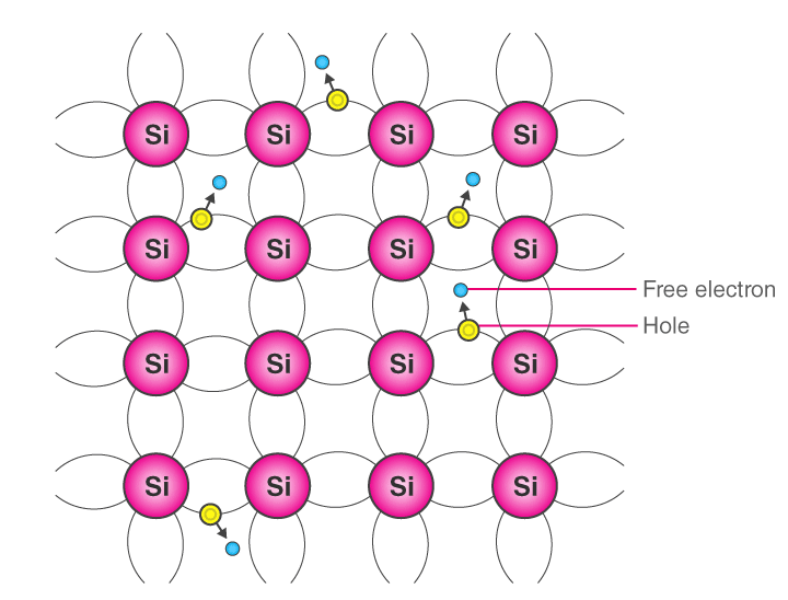
- In a pure semiconductor, the number of holes is equal to the number of electrons. Thermal agitation continues to produce new electron-hole pairs and these electron-hole pairs disappear because of recombination.
 Intrinsic Semiconductor
 - With each electron-hole pair created, two charge-carrying particles are formed. One is negative which is a free electron with mobility µn. The other is a positive i.e., hole with mobility µp. The electrons and hole move in the opposite direction in an electric field E, but since they are of opposite sign, the current due to each is in the same direction.
- Hence the total current density J within the intrinsic semiconductor is given by:
J = Jn + Jp
= q n µn E + q p µp E
= (n µn + p µp)qE
= σ E
Where n = No. of electrons/unit volume i.e., the concentration of free electrons
p = No. of holes/unit volume i.e., the concentration of holes
E = applied electric field strength, V/m
q = charge of electron or hole in Coulombs - Hence, σ is the conductivity of semiconductor which is equal to (n µn + p µp)q. The resistivity of semiconductor is reciprocal of conductivity.
Ρ = 1/ σ - It is evident from the above equation that current density within a semiconductor is directly proportional to applied electric field E.
- For a pure semiconductor, n = p = ni where ni = intrinsic concentration.
The value of ni is given by:
ni2 = AT3 exp (-EGO/KT)
Therefore, J = ni ( µn + µp) qE - Hence, conductivity in an intrinsic semiconductor is: σi = ni ( µn + µp) q
- Intrinsic conductivity increases at the rate of 5% per o C for Ge and 7% per o C for Si.
Conductivity in Extrinsic Semiconductor (N-Type and P-Type)

- The conductivity of an intrinsic semiconductor is given by:
σi = ni ( µn + µp) q
= (n µn + p µp)q - For N-type , n>>p
Therefore, σ = q n µn - For P-type, p>>n
Therefore, σ = q p µp
Try yourself: What type of material is obtained when an intrinsic semiconductor is doped with pentavalent impurity?MULTIPLE CHOICE QUESTION
Fermi Level
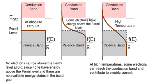
- The highest energy level that an electron can occupy at the absolute zero temperature is known as the Fermi Level. The Fermi level lies between the valence band and conduction band because at absolute zero temperature the electrons are all in the lowest energy state.

- Due to lack of sufficient energy at 0 Kelvin, the Fermi level can be considered as the sea of fermions (or electrons) above which no electrons exist. The Fermi level changes as the solids are warmed and as electrons are added to or withdrawn from the solid.
Charge Densities in P-Type and N-Type Semiconductor
- Mass Action Law: Under thermal equilibrium for any semiconductor, the product of the no. of holes and the concentration of electrons is constant and is independent of the amount of donor and acceptor impurity doping.
n.p = ni2
where n = electron concentration
p = hole concentration
ni2= intrinsic concentration - In N-type semiconductor as the no. of electrons increase, the no. of holes decreases. Similarly in P-type, as the no. of holes increases the no. of electrons decreases. Thus, the product is constant and is equal to ni2 in case of intrinsic as well as extrinsic semiconductor.
- The law of mass action has given the relationship between free electrons concentration and hole concentration. These concentrations are further related by the law of electrical neutrality, as explained below.
Try yourself: A p-type semiconductor has an acceptor density of 1020 atoms/m3 and intrinsic concentration of 2.5 × 10¹⁹ m-1 at 300K. The electron concentration in this p-type semiconductor isMULTIPLE CHOICE QUESTION
Law of Electrical Neutrality
- Semiconductor materials are electrically neutral. According to the law of electrical neutrality, in an electrically neutral material, the magnitude of positive charge concentration is equal to that of negative charge concentration.
- Let us consider a semiconductor that has ND donor atoms per cubic centimetre and NA acceptor atoms per cubic centimetre i.e., the concentration of donor and acceptor atoms are ND and NA, respectively.
- Therefore, ND positively charged ions per cubic centimetre are contributed by donor atoms and NA negatively charged ions per cubic centimetre are contributed by the acceptor atoms. Let n, p be concentration of free electrons and holes respectively. Then according to the law of neutrality,
ND + p = NA + n ...eq 1.1
For N-type semiconductor, NA = 0 and n>>p.
Therefore, ND ≈ n ...eq 1.2 - Hence for N-type semiconductor, the free electron concentration is approximately equal to the concentration of donor atoms. In later applications since some confusion may arise as to which type of semiconductor is under consideration at the given moment, the subscript n or p is added for N-type or P-type respectively. Hence eq 1.2 becomes ND ≈ nn.
- Therefore, the current density in N-type semiconductor is J = ND µn q E
and conductivity σ = ND µn q. - For P-type semiconductor, ND = 0 and p>>n.
Therefore NA ≈ p or NA ≈ pp. - Hence for P-type semiconductor, the hole concentration is approximately equal to the concentration of acceptor atoms.
Current density in N-type semiconductor is J = NA µp q E
And conductivity σ = NA µp q - Mass action law for N-type:
nn pn= ni2
pn = ni2/ ND since (nn≈ ND) - Mass action law for P-type:
np pp = ni2
np= ni2/ NA since (pp≈ NA)
The document Conductivity of Semiconductor is a part of Electronics and Communication Engineering (ECE) category.
All you need of Electronics and Communication Engineering (ECE) at this link: Electronics and Communication Engineering (ECE)
FAQs on Conductivity of Semiconductor
| 1. What is the conductivity of a semiconductor? |  |
Ans. The conductivity of a semiconductor refers to its ability to conduct electrical current. Unlike conductors, which have high conductivity, and insulators, which have low conductivity, semiconductors have an intermediate level of conductivity.
| 2. How is the conductivity of a semiconductor determined? |  |
Ans. The conductivity of a semiconductor is determined by its intrinsic properties, such as the number of charge carriers (electrons and holes) and their mobility. These factors can be influenced by doping the semiconductor with impurities or by applying an electric field.
| 3. Why is the conductivity of a semiconductor temperature-dependent? |  |
Ans. The conductivity of a semiconductor is temperature-dependent due to the effect of thermal energy on the movement of charge carriers. As temperature increases, the thermal energy causes more charge carriers to be excited, leading to increased conductivity.
| 4. What is the role of doping in semiconductor conductivity? |  |
Ans. Doping is the process of intentionally introducing impurities into a semiconductor to alter its electrical properties. By doping a semiconductor, the number of charge carriers can be controlled, thereby influencing its conductivity. Doping with donor impurities increases the number of free electrons, while doping with acceptor impurities increases the number of holes.
| 5. Can the conductivity of a semiconductor be modified? |  |
Ans. Yes, the conductivity of a semiconductor can be modified through various means. Doping is one way to alter the conductivity by introducing impurities. Additionally, applying an electric field or changing the temperature can also affect the conductivity of a semiconductor.
Download as PDF
Top Courses for Electronics and Communication Engineering (ECE)
Related Searches
video lectures, pdf , study material, Conductivity of Semiconductor, Conductivity of Semiconductor, mock tests for examination, MCQs, Objective type Questions, Sample Paper, Extra Questions, practice quizzes, Viva Questions, past year papers, Free, ppt, Previous Year Questions with Solutions, Summary, Semester Notes, Important questions, Conductivity of Semiconductor, shortcuts and tricks, Exam;


