Quantitative Theory of PN Junction Diode

PN JUNCTION WITH NO APPLIED VOLTAGE OR OPEN-CIRCUIT CONDITION
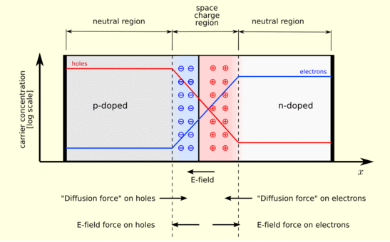
PN junction is formed when one side of a semiconductor is doped with an acceptor impurity (P-type) and the other side is doped with a donor impurity (N-type). The plane that separates the two doped regions is called the PN junction. In the N-type region the majority charge carriers are free electrons, while in the P-type region the majority carriers are holes.
At the junction there is an initial tendency for electrons to move (diffuse) from the N-side into the P-side, and for holes to diffuse from the P-side into the N-side. This process is called diffusion.

As electrons move from the N-side into the P-side they leave behind positively charged donor ions on the N-side. Electrons that enter the P-side recombine with holes and uncover negatively charged acceptor ions on the P-side. As a result a region near the junction becomes depleted of mobile charge carriers and acquires fixed space charge: positive in the N-side and negative in the P-side. This region is the depletion region, also called the space-charge region or transition region.
The fixed space charge creates an electric field directed from the positive charge on the N-side to the negative charge on the P-side. This electric field produces a force that opposes further diffusion of majority carriers; electrons on the N-side are repelled from the junction and holes on the P-side are repelled from the junction. An electrostatic potential difference builds up across the depletion region. This potential difference is known as the built-in potential, junction barrier, diffusion potential or contact potential and is denoted by V0.
The magnitude of the built-in potential depends on the doping concentrations and the temperature. Typical values at room temperature are V0 ≈ 0.72 V for silicon (Si) and V0 ≈ 0.30 V for germanium (Ge).
The depletion region typically has a thickness of the order of 0.5 μm for commonly used doping levels; its exact width depends on the relative doping of P and N regions and on V0. There are essentially no mobile carriers inside the depletion layer, so under open-circuit (zero external bias) the net current across the junction is zero. This occurs because diffusion currents of majority carriers are exactly balanced by the drift currents produced by the electric field in the depletion region.
Qualitative description of currents at equilibrium
- Diffusion current: Caused by concentration gradients; electrons diffuse from regions of high concentration (N) to low concentration (P) and holes diffuse from P to N.
- Drift current: Caused by the electric field in the depletion region; it drives minority carriers toward the junction where they recombine, opposing diffusion.
- Equilibrium condition: At thermal equilibrium the diffusion and drift currents cancel so that the net current is zero.
Charge density and electric field in the depletion region
Assuming an abrupt junction and the depletion approximation (all mobile carriers removed from the depletion region), the charge density ρ(x) is approximately equal to the fixed ion charge:
- ρ(x) = -q NA in the P-side depletion region (where acceptors are ionised)
- ρ(x) = +q ND in the N-side depletion region (where donors are ionised)
- ρ(x) = 0 outside the depletion region
The electric potential φ(x) in the depletion region follows Poisson's equation:
Poisson's equation:
d²φ/dx² = -ρ(x)/εs
where εs is the semiconductor permittivity and q is the electronic charge.
Derivation - depletion widths, built-in potential and maximum field
Using the depletion approximation and solving Poisson's equation across the depletion region gives the following standard relations.
Assumptions: The depletion region extends from x = -xp in the P-side to x = +xn in the N-side. The total depletion width is W = xp + xn.
Charge neutrality in depletion region:
q NA xp = q ND xn
Therefore:
xp = (ND / (NA + ND)) · W
xn = (NA / (NA + ND)) · W
Electric field (from integrating Poisson's equation):
E(x) is linear within each side of the depletion region and reaches a maximum magnitude at the metallurgical junction (x = 0). The maximum electric field Emax is
Emax = (q ND xn) / εs = (q NA xp) / εs
Potential difference across depletion region (built-in potential V0):
The built-in potential equals the integral of the electric field across the depletion region. Using the quadratic potential profiles obtained from Poisson's equation and the charge neutrality condition leads to
V0 = (q / (2 εs)) · (NA xp2 + ND xn2)
Combination of the above relations yields a closed form for the total depletion width
W = sqrt[ (2 εs V0 / q) · ( (NA + ND) / (NA ND) ) ]
For a one-sided junction (for example heavily doped P+, N lightly doped), an approximation can be made where most of the depletion occurs in the lightly doped side. For a P+-N junction with NA ≫ ND,
W ≈ sqrt( (2 εs V0) / (q ND) )
Built-in potential in terms of carrier concentrations:
Using carrier statistics and Fermi level alignment at equilibrium gives
V0 = (k T / q) · ln( (NA ND) / ni2 )
where k is Boltzmann's constant, T is absolute temperature and ni is the intrinsic carrier concentration of the semiconductor. This expression shows the dependence of the built-in potential on doping concentrations and temperature.
Energy-band picture and Fermi levels at equilibrium
Before contact, the Fermi energy in the N-type material lies nearer to the conduction band, while in the P-type it lies nearer to the valence band. After forming the junction and reaching thermal equilibrium, the Fermi level is constant throughout the device. Band bending occurs near the junction producing an energy barrier that prevents majority carriers from diffusing freely across the junction. The built-in potential V0 corresponds to the difference in electrostatic potential required to align the Fermi level across the junction.
Physical consequences and practical notes
- The depletion region contains immobile ionised dopants and therefore supports an electric field; mobile carriers are largely absent in this region.
- At equilibrium the net current across the diode is zero because drift and diffusion currents balance.
- The depletion width and built-in potential affect diode capacitance, breakdown voltage and the response of the diode to applied bias.
- Typical built-in potential values are about 0.72 V for silicon and 0.30 V for germanium at room temperature; the depletion width is typically about 0.5 μm for moderate doping levels.
Applications and relevance
- Rectifiers and switching diodes: Operation depends on forward and reverse bias of the PN junction and the characteristics derived from the depletion region.
- Diode capacitance (junction capacitance): The depletion region acts like a dielectric-filled capacitor whose capacitance changes with applied voltage; used in varactors.
- Photodiodes and solar cells: Photogenerated electron-hole pairs in or near the depletion region are separated by the junction field, producing photocurrent.
- LEDs and laser diodes: Recombination of injected carriers across the junction produces light; junction properties determine efficiency and wavelength.
Summary
The PN junction at zero applied voltage reaches thermal equilibrium where diffusion of carriers is balanced by drift due to the internal electric field. The resulting depletion region contains fixed space charge and supports a built-in potential V0 that depends on doping and temperature. Poisson's equation under the depletion approximation yields closed-form expressions for the depletion width, maximum electric field and the potential profile. These quantitative relations determine many important device parameters such as junction capacitance, breakdown voltage and the response to applied bias.
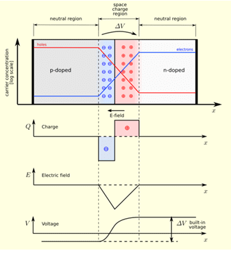 Fig. 1.8
FAQs on Quantitative Theory of PN Junction Diode
| 1. What is the quantitative theory of a PN junction diode? |  |
| 2. How does the PN junction diode work? | |
| 3. What are the important parameters in the quantitative theory of a PN junction diode? | |
| 4. How can the current-voltage characteristics of a PN junction diode be calculated using the quantitative theory? | |
| 5. What are the applications of the quantitative theory of PN junction diodes? | |


 | Explore Courses for Electrical Engineering (EE) exam |
 | Get EduRev Notes directly in your Google search |