Common Collector Amplifier - Electrical Engineering (EE) PDF Download
Common Collector Amplifier:
If a high impedance source is connected to low impedance amplifier then most of the signal is dropped across the internal impedance of the source. To avoid this problem common collector amplifier is used in between source and CE amplifier. It increases the input impedance of the CE amplifier without significant change in input voltage.
Fig. 1, shows a common collector (CC) amplifier. Since there is no resistance in collector circuit, therefore collector is ac grounded. It is also called grounded collector amplifier. When input source drives the base, output appears across emitter resistor. A CC amplifier is like a heavily swamped CE amplifier with a collector resistor shorted and output taken across emitter resistor.
vout = vin - VBE
Therefore, this circuit is also called emitter follower, because VBE is very small. As vin increases, vout increases.
If vin is 2V, vout = 1.3V
If vin is 3V, vout = 2.3V.
Since vout follows exactly the vin therefore, there is no phase inversion between input and output.
The output circuit voltage equation is given by-
VCE = VCC – IE RE
Since IE = IC
IC = (VCC – VCE ) / RE
This is the equation of dc load line. The dc load line is shown in Fig. 1.
Common Collector Amplifier
Voltage gain:
Fig. 2, shows an emitter follower driven by a small ac voltage. The input is applied at the base of transistor and output is taken across the emitter resistor. Fig. 3, shows the ac equivalent circuit of the amplifier. The emitter is replaced by ac resistance r'e.
The ac output voltage is given by
vout = RE ie
and, vin = ie (RE + r'e )Therefore, A = RE / ( RE +r'e )
Since r'e << RE
Av=1. (approx)
Therefore, it is a unity gain amplifier. The practical emitter follower circuit is shown in Fig. 4
The ac source (vS) with a series resistance RS drives the transistor base. Because of the biasing resistor and input impedance of the base, some of the ac signal is lost across the source resistor. The ac equivalent circuit is shown in Fig. 5.
The input impedance at the base is given by
The total input impedance of an emitter follower includes biasing resistors in parallel with input impedance of the base.
zin = R1 || R2|| (r'e + RE)
Since RE is very large as compared to R1 and R2.
Thus, zin ≈ R1 || R2
Therefore input impedance is very high.
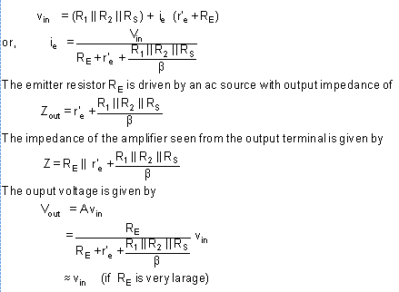
Applying Thevenin's theorem to the base circuit of Fig. 5, it becomes a source vin and a series resistance (R1 || R2 || RS ) as shown in Fig. 6.

Common Collector Amplifier
Example 1:
Find the Q-point of the emitter follower circuit of fig. 7 with R1 = 10 KΩ and R2 = 20 KΩ. Assume the transistor has a β of 100 and input capacitor C is very-very large.
Solution:
We first find the Thevenin's equivalent of the base bias circuitry.
RB = R1 || R2 = 6.67 K Ω
From the bias equation we have
Example - 2
Find the output voltage swing of the circuit of fig. 7.
Solution:
The Q-Point location has already been calculated in Example-1. We found that the quiescent collector current is 4.95 mA.
The Output voltage swing = 2 . IC peak . (RE || RLoad) = 2(4.95 x 10⁻³) (300) = 2.97V
This is less than the maximum possible output swing. Continuing the analysis,
VCEQ = VCC – ICQ RE = 9.03 V
VCC = VCEQ + ICQ (RE || RLoad ) = 10.5 V
The load lines for this problem are shown in Fig. 8.
fig. 8
FAQs on Common Collector Amplifier - Electrical Engineering (EE)
| 1. What is a common collector amplifier? |  |
| 2. How does a common collector amplifier work? |  |
| 3. What are the advantages of a common collector amplifier? |  |
| 4. What are the applications of a common collector amplifier? |  |
| 5. How to calculate the voltage gain of a common collector amplifier? |  |


