Test: Basic Electronics- 1 - Electrical Engineering (EE) MCQ
20 Questions MCQ Test - Test: Basic Electronics- 1
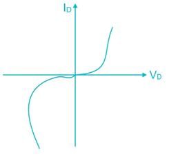
The reverse bias characteristics of semiconductor of a semiconductor diode is shown in
| 1 Crore+ students have signed up on EduRev. Have you? Download the App |
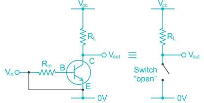
What are the ON/OFF terminals of a transistor when it is operated as a switch?
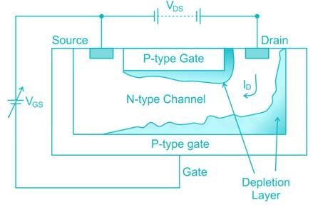
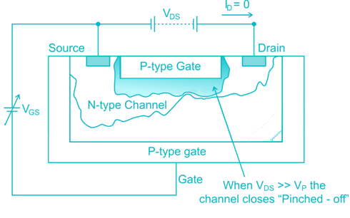
In JFET, the application of reverse bias to the gate terminals will cause the depletion layers to
Two p-n junction diodes are connected back to back to make a transistor. Which one of the following is correct?
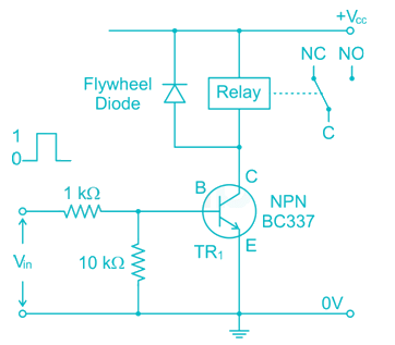
In an electronic circuit transistor is used for switching ON and OFF a relay when the transistor switches OFF the relay a higher voltage appears across the transistor. How can a transistor be protected from this voltage?
Transistor biasing is done to keep _______ in the circuit.
In an amplifier the maximum power transfer to the load resistance should be
What is the main source of distortion in a push-pull amplifier?
The bonding forces in compound semiconductors, such as GaAs, arise form
The Trans conductance of a JFET is computed at constant VDS by:
The intersection of the D.C. load line with the given base current curve is the
Which among the following will possess a higher bandwidth, if two transistors are provided with unity gain frequency?


