NEET Exam  >  NEET Test  >   Past Year Papers  >  31 Year NEET Previous Year Questions: Semiconductor Electronics - 3 - NEET MCQ

31 Year NEET Previous Questions: Semiconductor Electronics - 3 Free MCQ


MCQ Practice Test & Solutions: 31 Year NEET Previous Year Questions: Semiconductor Electronics - 3 (25 Questions)

You can prepare effectively for NEET NEET Past Year Papers with this dedicated MCQ Practice Test (available with solutions) on the important topic of "31 Year NEET Previous Year Questions: Semiconductor Electronics - 3". These 25 questions have been designed by the experts with the latest curriculum of NEET 2026, to help you master the concept.

Test Highlights:

  • - Format: Multiple Choice Questions (MCQ)
  • - Duration: 50 minutes
  • - Number of Questions: 25

Sign up on EduRev for free to attempt this test and track your preparation progress.

31 Year NEET Previous Year Questions: Semiconductor Electronics - 3 - Question 1

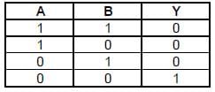
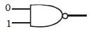
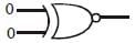
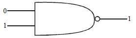
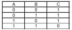
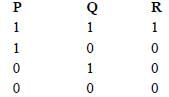
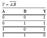
The following truth table belongs to which of the following four gates? [1997]


Detailed Solution: Question 1

The given truth table is of
(OR gate + NOT gate) ≡ NOR gate

31 Year NEET Previous Year Questions: Semiconductor Electronics - 3 - Question 2

A semi-conducting device is connected in aseries circuit with a battery and a resistance. Acurrent is found to pass through the circuit. Ifthe polarity of the battery is reversed, the currentdrops to almost zero. The device may be

Detailed Solution: Question 2

In reverse bias, the current through a p-n
junction is almost zero.

31 Year NEET Previous Year Questions: Semiconductor Electronics - 3 - Question 3

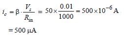
The transfer ratio β of a transistor is 50. Theinput resistance of the transistor when used inthe common emitter configuration is 1 kΩ. Thepeak value of the collector A.C. current for anA.C. input voltage of 0.01 V peak is [1998]

Detailed Solution: Question 3

31 Year NEET Previous Year Questions: Semiconductor Electronics - 3 - Question 4

Which of the following gates will have an output of 1?

(a)

(b)

(c)

(d)

Detailed Solution: Question 4

(a) is a NAND gate so output is 

(b) is a NOR gate so output is  

(c) is a NAND gate so output is 

(d) is a XOR gate so output is 

Following is NAND Gate

31 Year NEET Previous Year Questions: Semiconductor Electronics - 3 - Question 5

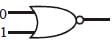
The truth-table given below is for which gate?   [1998]

Detailed Solution: Question 5

Relation between A, B and C shows that

31 Year NEET Previous Year Questions: Semiconductor Electronics - 3 - Question 6

The cause of the potential barrier in a p-n diodeis [1998]

Detailed Solution: Question 6

During the formation of a junction diode,
holes from p-region diffuse into n-region and
electrons from n-region diffuse into p-region.
In both cases, when an electron meets a hole,
they cancel the effect of each other and as a
result, a thin layer at the junction becomes
free from any of charge carriers. This is called
depletion layer. There is a potential gradient
in the depletion layer, negative on the p-side
and positive on the n-side. The potential
difference thus developed across the
junction is called potential barrier.

31 Year NEET Previous Year Questions: Semiconductor Electronics - 3 - Question 7

In forward bias, the width of potential barrier ina p-n junction diode [1999]

Detailed Solution: Question 7

We know that in forward bias of p-n junction
diode, when positive terminal is connected
to p-type diode, the repulsion of holes takes
place which decreases the width of potential
barrier by striking the combination of holes
and electrons.

31 Year NEET Previous Year Questions: Semiconductor Electronics - 3 - Question 8

A depletion layer consists of [1999]

Detailed Solution: Question 8

Depletion layer is formed by diffusion of
holes and electrons from p-type
semiconductor to n-type semiconductor and
vice-versa. Hence, donor and acceptor atom
get positive and negative charge leading to
formation of p-n junction. Thus, donor and
acceptor are immobile.

31 Year NEET Previous Year Questions: Semiconductor Electronics - 3 - Question 9

Which of the following when added acts as animpurity into silicon produced n-type semiconductor?    [1999]

Detailed Solution: Question 9

n-type of silicon semiconductor is formed
when impurity is mixed with pentavalent
atom. Out of given choices only phosphorus
is pentavalent.

31 Year NEET Previous Year Questions: Semiconductor Electronics - 3 - Question 10

In a junction diode, the holes are due to        [1999]

Detailed Solution: Question 10

Holes are produced due to missing of
electrons.

31 Year NEET Previous Year Questions: Semiconductor Electronics - 3 - Question 11

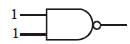
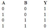
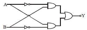
A gate has the following truth table

The gate is

Detailed Solution: Question 11

P, Q and R are related as R = P. Q which is
relation of AND gate.

31 Year NEET Previous Year Questions: Semiconductor Electronics - 3 - Question 12

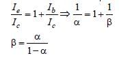
In the study of transistor as amplifier, if  and  , where, IC, IB and IE are the collector, base and emitter currents, then   [2000]

Detailed Solution: Question 12

As we know that Ie = Ic = Ib
Divide both side by Ie

31 Year NEET Previous Year Questions: Semiconductor Electronics - 3 - Question 13

The forward biased diode is            [2000]

Detailed Solution: Question 13

As A is at higher potential than B, hence
current will flow from A to B i.e. from p
junction to n junction and diode is forward
biased.

31 Year NEET Previous Year Questions: Semiconductor Electronics - 3 - Question 14

Which gate is represented by the following truth table ?

Detailed Solution: Question 14

Which is truth table of NAND gate

31 Year NEET Previous Year Questions: Semiconductor Electronics - 3 - Question 15

The intrinsic semiconductor becomes insulator at

[2001]

Detailed Solution: Question 15

At 0K, motion of free electrons stop. Hence
conductivity becomes zero. Therefore, at 0K
intrinsic semiconductor becomes insulator.

31 Year NEET Previous Year Questions: Semiconductor Electronics - 3 - Question 16

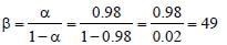
For a common emitter circuit if    then  current gain for common emitter circuit will be   [2001]

Detailed Solution: Question 16

We have, 

31 Year NEET Previous Year Questions: Semiconductor Electronics - 3 - Question 17

Transmission of light in optical fibre is due to         [2001]

Detailed Solution: Question 17

Light is trasmitted through optical fibre due
to multiple total internal reflections.

31 Year NEET Previous Year Questions: Semiconductor Electronics - 3 - Question 18

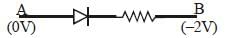
A d.c. battery of V volt is connected to a series combination of a resistor R and an ideal diode D as shown in the figure below. The potential difference across R will be [2002]

Detailed Solution: Question 18

In forward biasing, the diode conducts. for ideal junction diode, the forward resistance is zero; therefore, entire applied voltage occurs across external resistance R i.e. there occurs no potential drop, so potential across R is V in forward biased.

31 Year NEET Previous Year Questions: Semiconductor Electronics - 3 - Question 19

In a p-n junction     [2002]

Detailed Solution: Question 19

2: The n-side is at a higher electrical potential than the p-side.

In a p-n junction, a p-type semiconductor material is joined to an n-type semiconductor material. This creates a region called the depletion region, which is a region where the concentration of charge carriers (electrons and holes) is significantly lower than in the surrounding materials.

In equilibrium, the electrical potential of the p-side is lower than that of the n-side, due to the difference in the concentration of charge carriers. The electrical potential of the p-side is attracted to the higher concentration of holes on the p-side, while the electrical potential of the n-side is attracted to the higher concentration of electrons on the n-side. This creates an electrical potential difference across the p-n junction, with the n-side at a higher potential than the p-side.

Option 1 is incorrect because the potential of the p and n-sides does not alternate. Option 3 is incorrect because the p-side is at a lower potential than the n-side. Option 4 is incorrect because the p and n-sides are at different potentials. Therefore, the correct answer is 2: The n-side is at a higher electrical potential than the p-side.

31 Year NEET Previous Year Questions: Semiconductor Electronics - 3 - Question 20

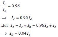
In the case of a common emitter transistoramplifier, the ratio of the collector current to theemitter current Ic /Ie is 0.96. The current gain ofthe amplifier is [2002]

Detailed Solution: Question 20

31 Year NEET Previous Year Questions: Semiconductor Electronics - 3 - Question 21

If a full wave rectifier circuit is operating from50Hz mains, the fundamental frequency in theripple will be     [2003]

Detailed Solution: Question 21

In case of full wave rectifier,
Fundamental frequency = 2 × mains
frequency
= 2 × 50 = 100Hz.

31 Year NEET Previous Year Questions: Semiconductor Electronics - 3 - Question 22

An n-p-n transistor conducts when [2003]

Detailed Solution: Question 22

When the collector is positive and emitter is
negative w.r.t. base, it causes the forward
biasing for each junction, which causes
conduction of current.

31 Year NEET Previous Year Questions: Semiconductor Electronics - 3 - Question 23

Barrier potential of a p-n junction diode doesnot depend on [2003]

Detailed Solution: Question 23

Barrier potential does not depend on diode
design while barrier potential depends upon
temperature, doping density, and forward
biasing.

31 Year NEET Previous Year Questions: Semiconductor Electronics - 3 - Question 24

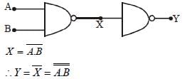
Following diagram performs the logic function of         [2003]

Detailed Solution: Question 24

Y = A. B by Demorgan therorem
∴ This diagram performs the function of
AND gate.

31 Year NEET Previous Year Questions: Semiconductor Electronics - 3 - Question 25

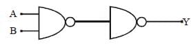
The following circuit represents         [1999]

Detailed Solution: Question 25

Output of upper AND gate = 

Output of lower AND gate = 

∴ Output of OR gate, Y = 

This is Boolean expression for XOR gate.

5 videos|87 docs|145 tests
Information about 31 Year NEET Previous Year Questions: Semiconductor Electronics - 3 Page
In this test you can find the Exam questions for 31 Year NEET Previous Year Questions: Semiconductor Electronics - 3 solved & explained in the simplest way possible. Besides giving Questions and answers for 31 Year NEET Previous Year Questions: Semiconductor Electronics - 3, EduRev gives you an ample number of Online tests for practice
5 videos|87 docs|145 tests
Download as PDF