31 Year NEET Previous Year Questions: Semiconductor Electronics - 1 - NEET MCQ
25 Questions MCQ Test - 31 Year NEET Previous Year Questions: Semiconductor Electronics - 1

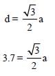
Sodium has body-centered packing. The distance between the two nearest atoms is 3.7 Å. The lattice parameter is:
[2009]
[2009]
Which one of the following statements is false?
[2010]
[2010]
| 1 Crore+ students have signed up on EduRev. Have you? Download the App |
Which one of the following bonds produces a solid that reflects light in the visible region and whose electrical conductivity decreases with temperature and has a high melting point?
[2010]
[2010]
The device that can act as a complete electronic circuit is:
[2010]
A common emitter amplifier has a voltage gain of 50, an input impedance of 100 Ω and an output impedance of 200 Ω. The power gain of the amplifier is:
[2010]


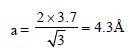
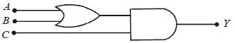
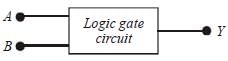
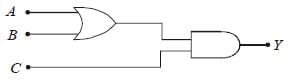
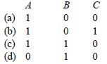
To get an output Y = 1 from the circuit shown below, the input must be:
[2010]

For transistor action:
(1) Base, emitter and collector regions should have similar size and doping concentrations.
(2) The base region must be very thin and lightly doped.
(3) The emitter-base junction is forward biased and the base-collector junction is reverse biased.
(4) Both the emitter-base junction as well as the base-collector junction are forward biased.
The following Figure shows a logic gate circuit with two inputs A and B and the output Y. The voltage waveforms of A, B and Y are given:
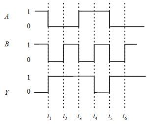
The logic gate is:
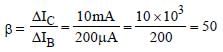
A transistor is operated in common emitter configuration at VC = 2V such that a change in the base current from 100 μA to 300 μA produces a change in the collector current from 10 mA to 20 mA. The current gain is:
[2011]
In forward biasing of the p–n junction:
[2011]
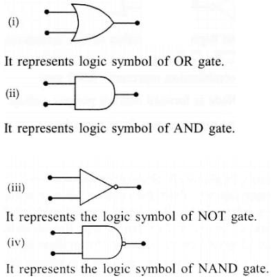
Symbolic representation of four logic gate are shown as: [2011]
(i)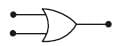
(ii)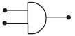
(iii)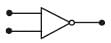
(iv)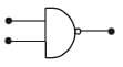
Pick out which ones are for AND, NAND and NOT gates, respectively.
If a small amount of antimony is added to germanium crystal then:
[2011]
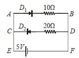
In the following figure, the diodes which are forward biased are:
[2011M]
(i)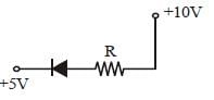
(ii)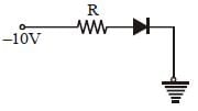
(iii)
(iv)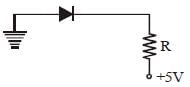
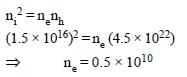
Pure Si at 500K has an equal number of electrons (ne) and hole (nh) concentrations of 1.5 × 10¹⁶ m–3. Doping by indium increases nh to 4.5 × 10²² m–3. The doped semiconductor is of:
[2011M]
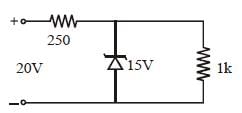
A Zener diode, having a breakdown voltage equal to 15V, is used in a voltage regulator circuit shown in the figure. The current through the diode is:
[2011M]

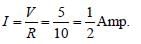
Two ideal diodes are connected to a battery as shown in the circuit. The current supplied by the battery is:
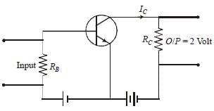
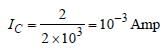
In a CE transistor amplifier, the audio signal voltage across the collector resistance of 2kΩ is 2V. If the base resistance is 1kΩ and the current amplification of the transistor is 100, the input signal voltage is:
[2012]
C and Si both have the same lattice structure, having 4 bonding electrons in each. However, C is an insulator whereas Si is an intrinsic semiconductor. This is because:
[2012]
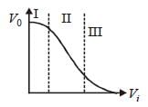
Transfer characteristics [output voltage (V0) vs input voltage (V1)] for a base biased transistor in CE configuration is as shown in the figure. For using a transistor as a switch, it is used:
[2012]
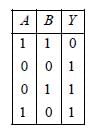
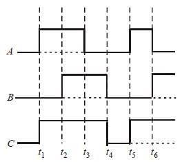
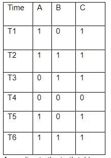
The figure shows a logic circuit with two inputs A and B and the output C. The voltage waveforms across A, B and C are given. The logic circuit gate is:
[2012]
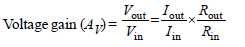
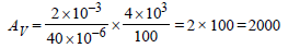
The input resistance of a silicon transistor is100 Ω. Base current is changed by 40 μA which results in a change in collector current by 2 mA. This transistor is used as a common emitter amplifier with a load resistance of 4 KΩ. The voltage gain of the amplifier is:
[2012M]
To get an output Y = 1 in the given circuit which of the following input will be correct:
[2012M]
In an n-type semiconductor, which of the following statement is true?
[2013]
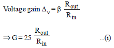
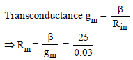
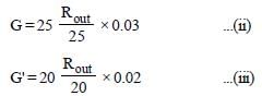
In a common emitter (CE) amplifier having a voltage gain G, the transistor used has transconductance 0.03 mho and a current gain of 25. If the above transistor is replaced with another one with transconductance 0.02 mho and a current gain of 20, the voltage gain will be:
[2013]

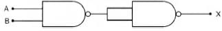
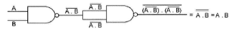
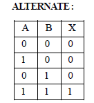
The output (X) of the logic circuit shown in figure will be:
Top Courses for NEET


Important Questions for 31 Year NEET Previous Year Questions: Semiconductor Electronics - 1
31 Year NEET Previous Year Questions: Semiconductor Electronics - 1 MCQs with Answers
Online Tests for 31 Year NEET Previous Year Questions: Semiconductor Electronics - 1
|
© EduRev
|
Education Revolution
|


|


