Electronics and Communication Engineering (ECE) Exam  >  Electronics and Communication Engineering (ECE) Tests  >  Test: Electronic Devices - 1 - Electronics and Communication Engineering (ECE) MCQ

Test: Electronic Devices - 1 - Electronics and Communication Engineering (ECE) MCQ


Test Description

10 Questions MCQ Test - Test: Electronic Devices - 1

Test: Electronic Devices - 1 for Electronics and Communication Engineering (ECE) 2024 is part of Electronics and Communication Engineering (ECE) preparation. The Test: Electronic Devices - 1 questions and answers have been prepared according to the Electronics and Communication Engineering (ECE) exam syllabus.The Test: Electronic Devices - 1 MCQs are made for Electronics and Communication Engineering (ECE) 2024 Exam. Find important definitions, questions, notes, meanings, examples, exercises, MCQs and online tests for Test: Electronic Devices - 1 below.
Solutions of Test: Electronic Devices - 1 questions in English are available as part of our course for Electronics and Communication Engineering (ECE) & Test: Electronic Devices - 1 solutions in Hindi for Electronics and Communication Engineering (ECE) course. Download more important topics, notes, lectures and mock test series for Electronics and Communication Engineering (ECE) Exam by signing up for free. Attempt Test: Electronic Devices - 1 | 10 questions in 30 minutes | Mock test for Electronics and Communication Engineering (ECE) preparation | Free important questions MCQ to study for Electronics and Communication Engineering (ECE) Exam | Download free PDF with solutions
Test: Electronic Devices - 1 - Question 1

Read the following statements regarding semiconductor and mark the incorrect answer.

  1. In P type semiconductor, holes as minority charge carrier
  2. In N type semiconductor, electron as majority charge carrier.
  3. It has conductivity in between the insulator and conductor.
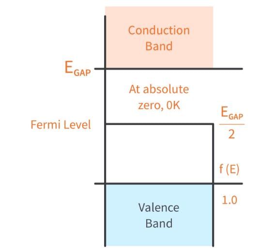
  4. At zero absolute temperature, intrinsic semiconductor behaves as a conductor.

Detailed Solution for Test: Electronic Devices - 1 - Question 1
  • The material which is not a good conductor, or a good insulator is called as a semiconductor.For example, silicon, germanium, etc.
  • The charge carriers which are present in more quantity in a semiconductor compared to other particles are called the majority charge carrier.
  • The impurity atoms added are called dopants and semiconductors doped with the impurity atoms are called extrinsic or doped semiconductors.
  • An ideal, perfectly pure semiconductor (with no impurities) is called an intrinsic semiconductor.
  • At absolute zero temperature valence band is full of electrons and the conduction band is empty, hence there are no free electrons in the conduction band and holes in the valence band.
  • The charge carrier concentration is zero at zero absolute temperature.
  • Hence, at zero absolute temperature the intrinsic semiconductor behaves like insulator.


There are two types of semiconductors:

P-type semiconductor:

  • The semiconductor having holes as majority charge carriers and electrons as a minority charge carrier is called a P-type semiconductor.


N-type semiconductor:

  • The semiconductor having electrons as majority charge carriers and holes as a minority charge carrier are called as N-type semiconductors.
Test: Electronic Devices - 1 - Question 2

The Fermi level in a semiconductor bar should:

Detailed Solution for Test: Electronic Devices - 1 - Question 2

Under equilibrium:

  • The fermi level across the entire material will be sum and does not vary with distance.
  • If there is any disturbance in the material, like junction contact, injection of impurities at any point, the charge carriers redistribute themselves such that the fermi-potential is same in entire material.

Under non-equilibrium:

  • The fermi level is uneven with gradient of charge distribution across distance, in material.
  • It can be studied using quasi-fermi states, related to charge distribution.
1 Crore+ students have signed up on EduRev. Have you? Download the App
Test: Electronic Devices - 1 - Question 3

Semiconductors have ______ conduction band and ______ valence band.

Detailed Solution for Test: Electronic Devices - 1 - Question 3

Property of Semiconductors:

  • Semiconductors are the materials that have a conductivity between conductors (generally metals) and non-conductors or insulators (such as ceramics).
  • Semiconductors can be compounds such as gallium arsenide or pure elements, such as germanium or silicon.
  • Semiconductors have an almost empty conduction band and an almost filled valence band.
  • In a semiconductor, the mobility of electrons is higher than that of the holes.
  • Its Resistivity lies between 10-5 to 106 Ωm
  • Conductivity lies between 105 to 10-6 mho/m
  • The temperature coefficient of resistance for semiconductors is Negative.
  • The current Flow in the semiconductor is mainly due to both electrons and holes.
*Answer can only contain numeric values
Test: Electronic Devices - 1 - Question 4

Hole mobility in Ge at room temperature is 1900 cm2/V-sec. The diffusion coefficient is ________cm2/sec.
(Write answer to one decimal point.) 

(Take kT = 25 mV)


Detailed Solution for Test: Electronic Devices - 1 - Question 4

Using the relation, D = 0.025 × 1900 cm2/sec
= 47.5 cm2/sec

Test: Electronic Devices - 1 - Question 5

The Difference between the donor energy level and fermi level in a n-type semiconductor in where 25% of the atoms are ionised at 300 k is:

Detailed Solution for Test: Electronic Devices - 1 - Question 5

As 25% of donor atoms are ionised, the occupation probability of donor level is 0.75.

ED - EF = -0.028 eV

*Answer can only contain numeric values
Test: Electronic Devices - 1 - Question 6

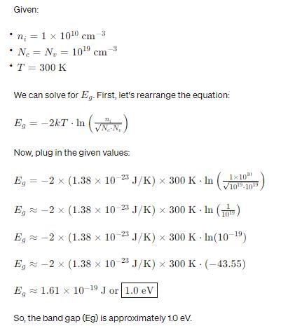
A semiconductor with intrinsic carrier concentration 1 × 1010 cm-3 at 300°K has both valence and conduction band effective densities of states NC and NV equal to 1019 cm-3. The band gap Eg is _____ eV. (Write answer to one decimal point.) 


Detailed Solution for Test: Electronic Devices - 1 - Question 6

*Answer can only contain numeric values
Test: Electronic Devices - 1 - Question 7

In a very long p-type Si bar with doping concentration Na = 1017 cm-3, excess holes are injected such that excessive concentration of holes at x = 0 is 5 × 1016 cm-3. The hole concentration at x = 1 μm is _____ × 1017 cm-3. Take μp = 500 cm2/v-s and recombination time constant τ = 10-8 s, kT = 0.0259 eV (Write answer to two decimal point.) 


Detailed Solution for Test: Electronic Devices - 1 - Question 7

Diffusion constant: 

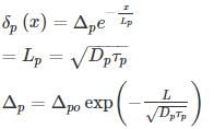
Diffusion length: 

  • Hole concentration at any distance x is sum of equillibrium and excess hole concentration excess hole concentration varies with the distance x as Δp e-x/Lp
  • p = p + Δp e-x/Lp
    Where po = Doping concentration
    Δp = extra hole concentration
    = (1+.379) x 1017
    1.379 × 1017 cm-3
Test: Electronic Devices - 1 - Question 8

In an intrinsic semiconductor, the Fermi energy level EF doesn’t lie in the middle of the band gap cause:

Detailed Solution for Test: Electronic Devices - 1 - Question 8
  • In an intrinsic semi-conductor the Fermi energy:Where NC and NV are density of state in valence and conduction bond respectively.
  • Since NC ∝ mn, effective mass of electron and Nv ∝ mp, effective mass of hole. Since mn and mp are not equal: 
Test: Electronic Devices - 1 - Question 9

A silicon bar is doped with donor impurities ND = 2.25 × 1015 cm-3. If the electron mobility μn = 1000 cm2/v-s then the approximate value of resistivity of silicon bar assuming partial ionization of 55% is __________ (Ω - cm)

Detailed Solution for Test: Electronic Devices - 1 - Question 9

Given ND = 2.25 × 1015 cm-3

Partial ionization of 55%, number of electrons is:

⇒ n = 0.55 × 2.25 × 1015 cm-3

= 1.2375 × 1015 cm-3

Electron mobility μn = 1000 cm2/v-s

Resistivity of n-type silicon = 

= 5.05 Ω – cm

Test: Electronic Devices - 1 - Question 10

Holes are injected into n-type Ge so that the at the surface of the semiconductor hole concentration is 1014/cm3. If diffusion constant of a hole in Ge is 49cm2/sec and minority carrier lifetime is τp = 10-3 sec. Then the hole concentration Δp at a distance of 4mm from the surface is ______1014/cm3.

Detailed Solution for Test: Electronic Devices - 1 - Question 10


= 1.6 × 10¹³/cm3

= 0.16 × 10¹⁴/cm3

Information about Test: Electronic Devices - 1 Page
In this test you can find the Exam questions for Test: Electronic Devices - 1 solved & explained in the simplest way possible. Besides giving Questions and answers for Test: Electronic Devices - 1, EduRev gives you an ample number of Online tests for practice

Top Courses for Electronics and Communication Engineering (ECE)

Download as PDF

Top Courses for Electronics and Communication Engineering (ECE)