GATE ECE (Electronics) Test: Electronic Devices - 3 Free Online Test 2026
MCQ Practice Test & Solutions: Test: Electronic Devices - 3 (10 Questions)
You can prepare effectively for Electronics and Communication Engineering (ECE) GATE ECE (Electronics) Mock Test Series 2027 with this dedicated MCQ Practice Test (available with solutions) on the important topic of "Test: Electronic Devices - 3". These 10 questions have been designed by the experts with the latest curriculum of Electronics and Communication Engineering (ECE) 2026, to help you master the concept.
Test Highlights:
- - Format: Multiple Choice Questions (MCQ)
- - Duration: 30 minutes
- - Number of Questions: 10
Sign up on EduRev for free to attempt this test and track your preparation progress.

The open-circuit p-n junction diode without any Biasing is shown if NA = 2 × 10¹⁷/cm3, ND = 5 × 10¹⁶/cm3 then the depletion region width (W) is ______μm
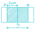
Detailed Solution: Question 1
Which of the following statements is TRUE for the function f(z) = z sin(z) / (z - π)²?
Detailed Solution: Question 2

The correct output waveform for the circuit shown if the input is a sinusoidal signal of maximum Amplitude Vmax is
The correct output waveform for the circuit shown if the input is a sinusoidal signal of maximum Amplitude Vmax is
Detailed Solution: Question 3
In the circuit shown, the forward biased LED has a voltage drop of 1.5 volts. If the battery voltage is 6V. Then the power displaced in the resistor R in milliwatts is _________mW. Current through LED is 15mA.
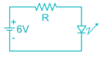
Detailed Solution: Question 4
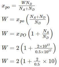
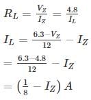
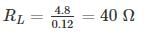
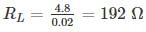
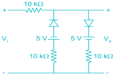
The voltage regulator circuit using a Zener diode is shown. The Zener diode current is limited in the range 5 ≤ iz ≤ 100 mA
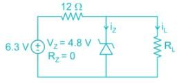
The range of load resistance is
The range of load resistance is
Detailed Solution: Question 5
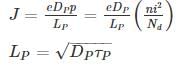
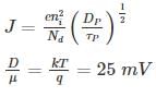
For a P±n Si junction the reverse current at room temperature is 0.9 nA/cm2. If donor density is 1015 cm-3 and intrinsic carrier concentration is 1.05 × 10¹⁰. The minority carrier life time is ________ n sec.
[Assume μP = 450 cm2/V-sec, kT = 25mV ]
Detailed Solution: Question 6
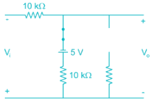
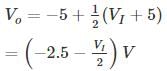
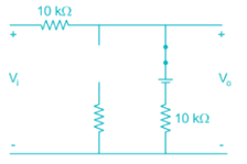
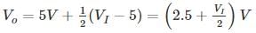
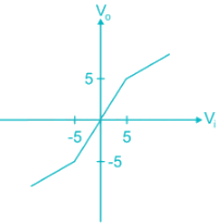
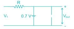
The sketch of output voltage Vo vs. input voltage VI is of from
Detailed Solution: Question 7
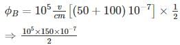
Consider a pn junction at zero bias with an electric distribution as sketched below. Calculate the built-in-potential
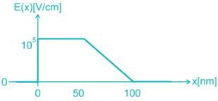
Detailed Solution: Question 8
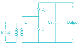
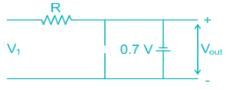
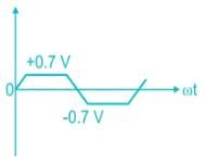
The correct waveform of the output of the given circuit is
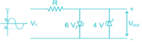
Assume the Zener diodes are ideal with threshold voltage Vk = 0.7
Detailed Solution: Question 9
The correct statement regarding depletion and diffusion capacitance is
i) Depletion capacitance is dominant in reverse-bias voltage
ii) Diffusion capacitance is dominant in reverse-bias voltage
iii) The diffusion capacitance is due to a stored charge of minority electrons and minority holes near the depletion region
iv) Depletion capacitance is directly proportional to the width of the depletion region
Detailed Solution: Question 10
26 docs|263 tests |