GATE ECE (Electronics) Test: Electronic Devices - 5 Free Online Test 2026
MCQ Practice Test & Solutions: Test: Electronic Devices - 5 (10 Questions)
You can prepare effectively for Electronics and Communication Engineering (ECE) GATE ECE (Electronics) Mock Test Series 2027 with this dedicated MCQ Practice Test (available with solutions) on the important topic of "Test: Electronic Devices - 5". These 10 questions have been designed by the experts with the latest curriculum of Electronics and Communication Engineering (ECE) 2026, to help you master the concept.
Test Highlights:
- - Format: Multiple Choice Questions (MCQ)
- - Duration: 30 minutes
- - Number of Questions: 10
Sign up on EduRev for free to attempt this test and track your preparation progress.

The figure shows the VTC characteristics of an NMOS inverter with three varying resistive loads (R).
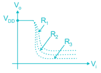
The correct statement is:
The correct statement is:
Detailed Solution: Question 1
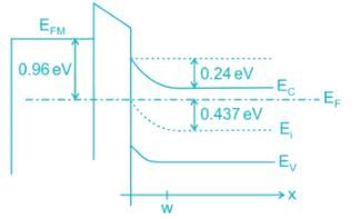
Assume that the zero for electrostatic potential is in the semiconductor bulk at large x and that there is no metal semiconductor work function difference. The relative dielectric constant for the oxide is ϵr = 11.8. If the intrinsic concentration is 1010/cm3. The doping density ND is _____ × 1017/cm3 (KT = 0.026 V)
Detailed Solution: Question 2

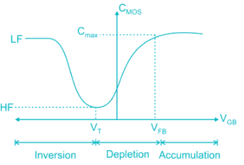
The figure shows MOS capacitor variation with applied gate voltage for n-type body/substrate.
The flat band voltage is:
The flat band voltage is:
Detailed Solution: Question 3
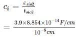
The insulator capacitance Ci of an ideal MOS capacitor with 10-nm gate oxide (εr = 3.9) on p-type Si with Na = 1016 cm-3 is ________ × 10-7 F/cm2
Detailed Solution: Question 4
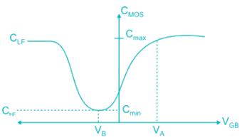
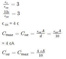
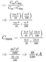
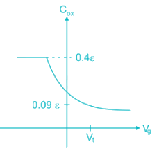
Which of the following curves represents the correct C – V characteristics of an NMOS transistor having an oxide layer thickness of 10 nm and a maximum depletion thickness of 100 nm. [Assume ϵs = permittivity of semiconductor, ϵox = permittivity of oxide and 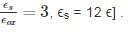
Detailed Solution: Question 5
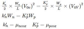
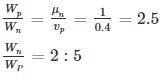
The mobility of hole is 0.4 times the mobility of electron. What must be the ratio of width of n-channel to p-channel MOSFET if they are to have equal drain currents when operated in saturation mode with same magnitude of overdrive voltage:
Detailed Solution: Question 6
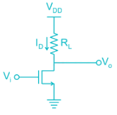
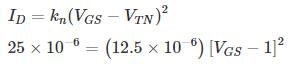
The circuit shown uses an NMOS transistor to implement a current source. For the transistor VTN = 1V and 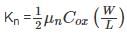 =12.5 uA/V2. The required value of VGS to get IDC = 25 μA and corresponding compliance voltage is:
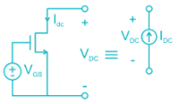
=12.5 uA/V2. The required value of VGS to get IDC = 25 μA and corresponding compliance voltage is:Detailed Solution: Question 7
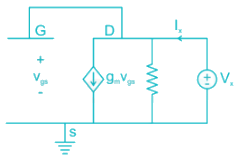
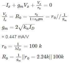
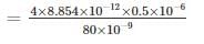
The output resistance R0 of the NMOS circuit if ID = 0.5 mA, λ = 0.02 V-1, 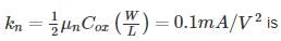 _____ kilo ohms.

_____ kilo ohms.Detailed Solution: Question 8

For a MOSFET with gate plate area 0.5 × 10⁻² cm2 and oxide layer thickness 80 nm, the value of MOS capacitance and its break down voltage are: (assume relative di-electric constant of sio2, ϵr = 4 and ϵ0 = 8.854 × 10⁻¹⁴ F/cm and dielectric strength of sio2 film is 5 × 10⁶ V/cm)
Detailed Solution: Question 9

 greater than dielectric strength (5 × 10⁶ V/cm)
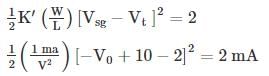
In the circuit shown in Figure, Transistors are characterized by 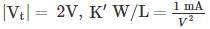 and λ = 0
The output voltage V0 is _______V
and λ = 0The output voltage V0 is _______V
Detailed Solution: Question 10
26 docs|263 tests |