Analog Electronics - 3 - Electronics and Communication Engineering (ECE) MCQ
10 Questions MCQ Test - Analog Electronics - 3

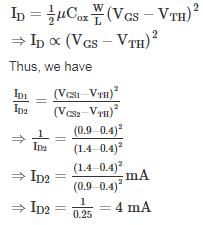
When the gate-to-source voltage VGS of a MOSFET with a threshold voltage of 400mV, working in saturation is 900mV, the drain current is observed to be 1mA. Neglecting the channel width modulation effect and assuming that the MOSFET is operating at saturation, the drain current for an applied VGS of 1400mV is
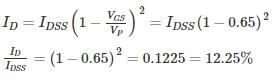
What percentage of current IDSS is the drain current for a JFET, if the gate to source voltage is 65% of the pinch-off voltage.

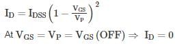
The ‘Pinch-off’ voltage of a JFET is 4 V. Then the off gate voltage of JFET is
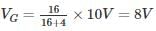
A MOSFET operating in saturation mode is shown in the below figure. The drain current is given as ID = ½ (VGS – 0.75)2 mA If VS = 5V, then the value of RS in kΩ is __________
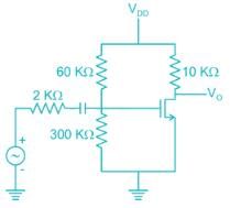
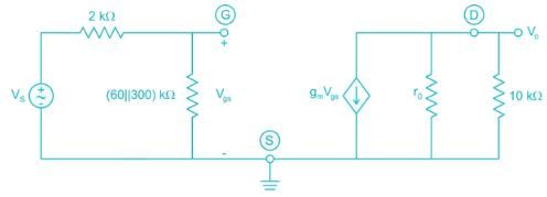
For the amplifier shown below, the drain current changes from 5 mA to 7 mA when the gate voltage D changed from -4.0 V to -3.7 V. The voltage gain of the amplifier is _____

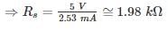
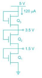
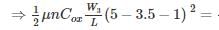
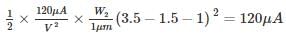
The NMOS transistors in the circuit below have VT = 1 V, μncox = 120 μA/V2, λ = 0 and L1 = L2 = L3 = 1 μm. The values of width of each of Q1, Q2, Q3 such that the voltage values are as shown in below figure are


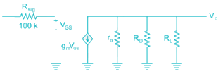
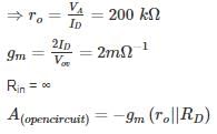
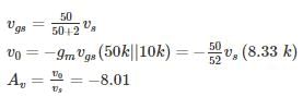
A common source amplifier biased at ID = 0.25 mA with RD = 20 kΩ and early voltage VA = 50 V and overdrive voltage (VGS – VT)DC = 0.25 V. If the input is fed through 100 kΩ and output are taken from 20 kΩ loads then the overall gain of the amplifier is _____ V/V.
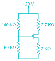
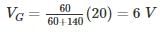
The transistor I the circuit is shown below has parameters IDSS = 8 mA and VP = -4 V. The value of VDS is___
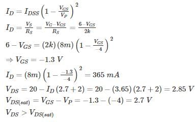
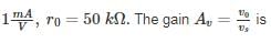
The small signal resistance (dVC/dID) of the n-channel MOSFET shown in figure below at bias voltage VC = 2V is (in kΩ) _________
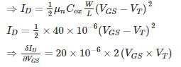
Given μnCox W/L = 40μ A/V2
VT = 1 V


Important Questions for Analog Electronics - 3
Analog Electronics - 3 MCQs with Answers
Online Tests for Analog Electronics - 3
|
© EduRev
|
Education Revolution
|


|


