Electrical Engineering (EE) Exam  >  Electrical Engineering (EE) Tests  >  Test: Logic Families - 2 - Electrical Engineering (EE) MCQ

Test: Logic Families - 2 - Electrical Engineering (EE) MCQ


Test Description

15 Questions MCQ Test - Test: Logic Families - 2

Test: Logic Families - 2 for Electrical Engineering (EE) 2024 is part of Electrical Engineering (EE) preparation. The Test: Logic Families - 2 questions and answers have been prepared according to the Electrical Engineering (EE) exam syllabus.The Test: Logic Families - 2 MCQs are made for Electrical Engineering (EE) 2024 Exam. Find important definitions, questions, notes, meanings, examples, exercises, MCQs and online tests for Test: Logic Families - 2 below.
Solutions of Test: Logic Families - 2 questions in English are available as part of our course for Electrical Engineering (EE) & Test: Logic Families - 2 solutions in Hindi for Electrical Engineering (EE) course. Download more important topics, notes, lectures and mock test series for Electrical Engineering (EE) Exam by signing up for free. Attempt Test: Logic Families - 2 | 15 questions in 45 minutes | Mock test for Electrical Engineering (EE) preparation | Free important questions MCQ to study for Electrical Engineering (EE) Exam | Download free PDF with solutions
Test: Logic Families - 2 - Question 1

Which of the following gates is NOT universal?

Detailed Solution for Test: Logic Families - 2 - Question 1

Universal Logic Gates:- In addition to the NOT, AND, OR, and XOR gates, three more common gates are available. These are identical to AND, OR, and XOR, except that the gate output has been negated. These gates are called NAND ('Not AND'), NOR ('Not OR'), and XNOR ('eXclusive Not OR').
NAND gate output is defined as  and similarly,
NOR gate output is defined as, 
NAND and NOR gates are also called Universal Logic Gates.
The reason being that all the basic logic gates (NOT, AND, and OR) can be realized using NAND/NOR gates only.

Test: Logic Families - 2 - Question 2

Which of the following IC logic families has minimum value of fan-out? 

Detailed Solution for Test: Logic Families - 2 - Question 2

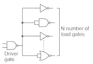
​Fan-out:

  • Fan-out is defined as the maximum number of inputs of the same IC family that a gate can drive without falling outside the specified output voltage limits.
  • Higher the fan-out, the higher the current supplying capacity of a gate.
  • For example, a fan-out of 5 indicates that the gate can drive (supply current to) at the most 5 inputs of the same IC family.
  • CMOS has the highest fan out.
  • Standard TTL has the lowest fan out.

1 Crore+ students have signed up on EduRev. Have you? Download the App
Test: Logic Families - 2 - Question 3

Which of the following IC logic families has the highest fan-out?

Detailed Solution for Test: Logic Families - 2 - Question 3

While choosing a particular digital IC for an application, its specifications or characteristics should be taken into account.
The main specifications for logic families are as follows:
Fan-in: The number of inputs that can be connected to a logic gate is called its ‘Fan-in’.
Fan-out: The number of units that can be connected to the output of a logic gate is called its ‘Fan-out’.
CMOS has the highest fan-out among the given logic families.
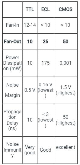
A comparison of the given logic families is as shown: 

Test: Logic Families - 2 - Question 4

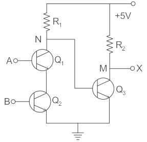
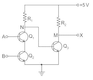
If A and B are the logical inputs to the following circuit, determine the logical relation between the inputs and the output X.
Detailed Solution for Test: Logic Families - 2 - Question 4

Concept:

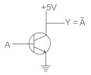
  • In a Common Emitter transistor, if input A is at low potential (Logic0) than, there is no voltage drop across Base Emitter junction and hence no current will flow through the Transistor (Cut Off state). therefore output is at high potential (Logic1).
  • In a Common Emitter transistor, if input A is at high potential (Logic1) than, there will be a voltage drop across Base Emitter junction and hence current will flow through the Transistor (Saturation state). therefore output is at low potential (Logic0).

Application:

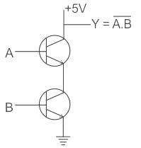
⇒ It can be NOT or NAND (because the output is inversion of input in these two cases)

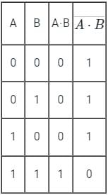
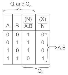
⇒ NAND Gate (output is inversion of product of both the inputs)


Now,


∴ Output, X = A⋅B

Test: Logic Families - 2 - Question 5

A particular logic family has VOH = 5 V, VOL = 1 V, VIH = 3.5 V and VIL = 2 V. The noise margin values NMH and NML will be

Detailed Solution for Test: Logic Families - 2 - Question 5

Concept:

Noise Margin
It is the amount of noise that can be allowed without disturbing the normal operation of the logic gates.

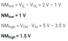
NMlow = VIL – VOL

NMhigh = VOH - VIH

Calculation:
Given voltage levels are VIL = 2 V  VOL = 5 V, VOH = 5 V, VIH = 3.5 V

Test: Logic Families - 2 - Question 6

Which among the following is the fastest switching logic family?

Detailed Solution for Test: Logic Families - 2 - Question 6

Emitter-coupled-logic (ECL):

  • Emitter-coupled-logic (ECL) is a BJT logic family that is generally considered the fastest logic available.
  • ECL achieves its high-speed operation by employing a relatively small voltage swing and preventing the transistors from entering the saturation region. (Reduces the storage delay time).
  • ECL transistor uses differential amplifier configuration as shown:

Test: Logic Families - 2 - Question 7

Which of the following logic families requires maximum power?

Detailed Solution for Test: Logic Families - 2 - Question 7

DCTL:

  • No external biasing required
  • Since no loading resistor present in the circuit cause low power consumption and very high packing density.
  • Also known as integrated injection circuit (I2C)
  • Current hogging takes place in DCTL
     

ECL:

  • Fastest logic circuit available
  • Highest power consumption.
  • Do not operate in the saturation region
  • Also known as current mode logic.
  • ECL is used in clock distribution circuits and other high-frequency applications.
     

I2L (integrated injection logic):

  • It is having the best figure of merit (1 Pico joule) among logic families.
  • It is having BJT of multiple collectors.
  • Due to the absence of a resistor, it uses a small chip area and small power consumption.
Test: Logic Families - 2 - Question 8

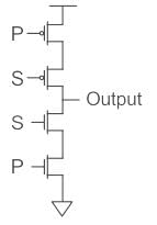
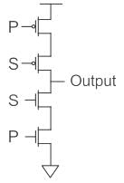
Output of the circuit shown below when S = 1 and S = 0 will be _____.
Detailed Solution for Test: Logic Families - 2 - Question 8

Concept:

Complementary Metal-oxide-semiconductor (CMOS) uses complementary & symmetrical pair of P-type & n-type MOSFETS.

  • The two important characteristics of CMOS devices are high noise immunity and low power dissipation.
  • In CMOS, during static operation at a time, only one MOS is ON i.e. either PMOS or NMOS. So there is no direct path from the power supply to the ground. Hence, Power dissipation in CMOS is low in static operation but it has high power dissipation in dynamic operation.

Calculation:

As the given figure is of CMOS with two inputs.

The upper part is PMOS which is switched on when 0 is applied and NMOS is switched on when 1 is applied.


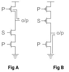
1. When S = 0 is applied, the PMOS connected to S (upper one) will be shorted and P at PMOS will appear across the output in complemented form as shown in fig(A).
So Output = P̅

2. Now when S = 1 is applied, the NMOS connected to S (lower one) will be shorted, and due to which ground will appear across the output and the circuit will go in a high impedance state as shown in fig(B).
Hence option (2) is the correct answer.

Test: Logic Families - 2 - Question 9

What is meant by the fan-out of a logic gate?

Detailed Solution for Test: Logic Families - 2 - Question 9

While choosing a particular digital IC for an application, its specifications or characteristics should be taken into account.
The main specifications for logic families are as follows:
Fan-in: The number of inputs that can be connected to a logic gate is called its ‘Fan-in’.
Fan-out: The number of units that can be connected to the output of a logic gate is called its ‘Fan-out’.

Test: Logic Families - 2 - Question 10

For a typical CMOS process, the minimum feature size is set to be 25 μm. The minimum line width at the process is set to be ______

Detailed Solution for Test: Logic Families - 2 - Question 10

Concept:

  1. Feature Size: The minimum feature size is the size or the width at which a transistor or any type of material on the silicon surface can be drawn at.
  2. If the minimum feature size can be reduced, this means that the transistor length can be reduced effectively making the transistor smaller with the same electrical properties.
  3. This allows for lower current flow between the junction for the same purpose and lesser heat dissipation.

The minimum line width is 2 × minimum feature size  ---(1)

Calculation:
Given:
Minimum feature size = 25 μm
Now the minimum line width can be calculated from equation (1)
Minimum line width = 2 × 25 μm
Minimum line width = 50 μm 
Hence option (3) is the correct answer.

Test: Logic Families - 2 - Question 11

The main advantage of CMOS is its

Detailed Solution for Test: Logic Families - 2 - Question 11

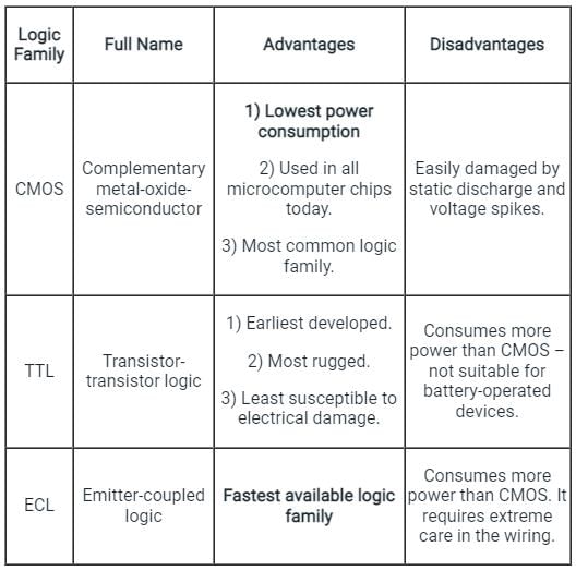
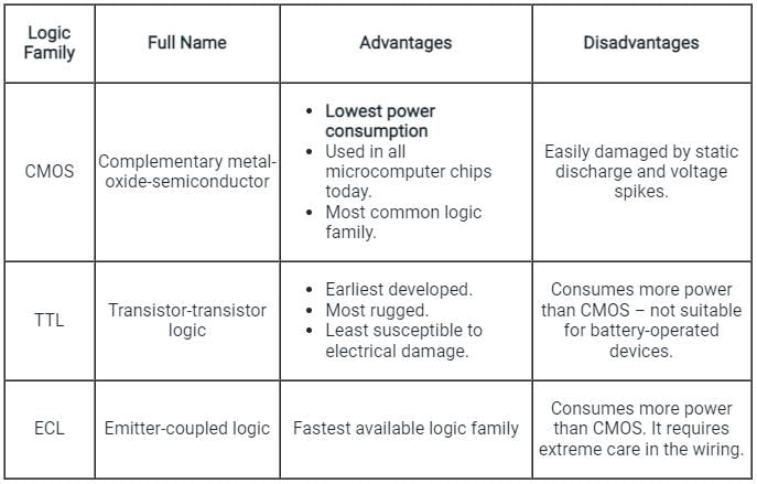
The most important parameters for evaluating and comparing logic families are:

  • Power dissipation
  • Propagation delay
  • Noise margin
  • Fan-out (loading)

General comparison of three commonly available logic families is explained in the following table:

Test: Logic Families - 2 - Question 12

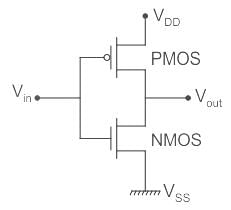
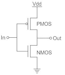
The above circuit acts as:

Detailed Solution for Test: Logic Families - 2 - Question 12

Inverter

  • This is equal to NOT gate in the digital circuitry.
  • The output of this is a compliment of the input.


This can be built from the transistors like BJT, MOSFET, etc…

The CMOS inverter consists of the NMOS and the PMOS field-effect transistors connected in one below the other.


When In = Low
PMOS will be shorted and output will be High.
When In = High
NMOS will be shorted and output will be Low.
Hence it acts as an inverter.

Test: Logic Families - 2 - Question 13

Which of the following logic gates can be used to implement the functionality of any logic gate?

Detailed Solution for Test: Logic Families - 2 - Question 13

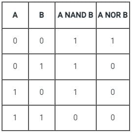
Two universal gates are NAND and NOR.

NAND:
In this gate, output of logic gate is false only when both the inputs are true. It is the complement of AND gate.
NOR gate: Output of this logic gate is true when both inputs are false.
Truth Table:

Test: Logic Families - 2 - Question 14

A unipolar logic family uses only ________ devices.

Detailed Solution for Test: Logic Families - 2 - Question 14


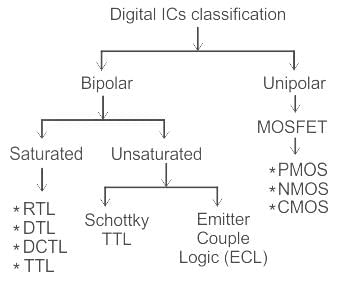
Unipolar Logic Families:

  • The device in which the conduction of current is due to either majority carrier or minority carrier is called Unipolar.
  • It mainly uses Unipolar devices like MOSFET.
  • These logic families have the advantages of high speed and lower power consumption than Bipolar families.

These are classified as:

  • PMOS or P-Channel MOS Logic Family
  • NMOS or N-Channel MOS Logic Family
  • CMOS Logic Family
Test: Logic Families - 2 - Question 15

Calculate the fan out of a TTL circuit with the following specifications:

IOL(max) = 32 mA, IIL(max) = 1.6 mA, IOH(max) = 400 uA, IIH(max) = 10 uA

Detailed Solution for Test: Logic Families - 2 - Question 15

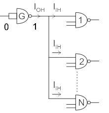
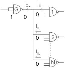
Fanout

  • It is the number of Standard loads (input current of the driven gate), the output of a gate to the same logic family.

Fanout high


Let IOH = 200 μA and IIH = 40 μA
G can drive 5 standard loads.

Fanout low


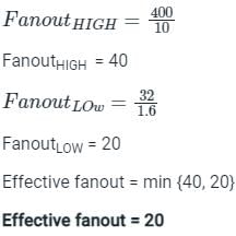
Effective Fanout = min (FanoutHIGH , FanoutLOW)

Calculation:
Given IOL(max) = 32 mA, IIL(max) = 1.6 mA, IOH(max) = 400 uA, IIH(max) = 10 uA

Information about Test: Logic Families - 2 Page
In this test you can find the Exam questions for Test: Logic Families - 2 solved & explained in the simplest way possible. Besides giving Questions and answers for Test: Logic Families - 2, EduRev gives you an ample number of Online tests for practice

Top Courses for Electrical Engineering (EE)

Download as PDF

Top Courses for Electrical Engineering (EE)