Electrical Engineering (EE) Exam  >  Electrical Engineering (EE) Tests  >  Test: FET Amplifier - 2 - Electrical Engineering (EE) MCQ

Test: FET Amplifier - 2 - Electrical Engineering (EE) MCQ


Test Description

15 Questions MCQ Test - Test: FET Amplifier - 2

Test: FET Amplifier - 2 for Electrical Engineering (EE) 2024 is part of Electrical Engineering (EE) preparation. The Test: FET Amplifier - 2 questions and answers have been prepared according to the Electrical Engineering (EE) exam syllabus.The Test: FET Amplifier - 2 MCQs are made for Electrical Engineering (EE) 2024 Exam. Find important definitions, questions, notes, meanings, examples, exercises, MCQs and online tests for Test: FET Amplifier - 2 below.
Solutions of Test: FET Amplifier - 2 questions in English are available as part of our course for Electrical Engineering (EE) & Test: FET Amplifier - 2 solutions in Hindi for Electrical Engineering (EE) course. Download more important topics, notes, lectures and mock test series for Electrical Engineering (EE) Exam by signing up for free. Attempt Test: FET Amplifier - 2 | 15 questions in 45 minutes | Mock test for Electrical Engineering (EE) preparation | Free important questions MCQ to study for Electrical Engineering (EE) Exam | Download free PDF with solutions
Test: FET Amplifier - 2 - Question 1

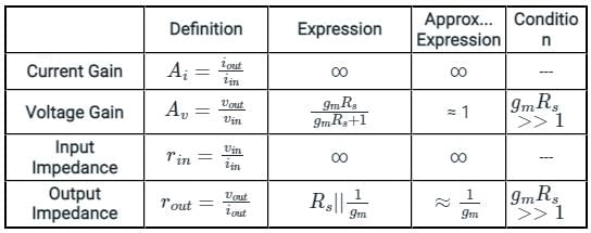
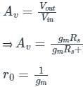
In a CD JFET configuration, if r0 = 1 / gm then:

Detailed Solution for Test: FET Amplifier - 2 - Question 1

JFET common drain amplifier is sometimes considered as a source follower and has voltage gain less than unity.

Putting the value of gm, we get

Test: FET Amplifier - 2 - Question 2

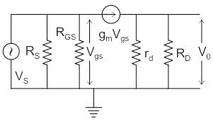
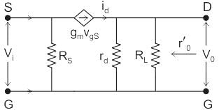
The given circuit represents small signal model of:

Detailed Solution for Test: FET Amplifier - 2 - Question 2

Common Gate FET Amplifier:

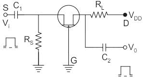
In this amplifier configuration, the input signal is applied to the source terminal, and output is taken from the drain as shown in Fig.

The gate is grounded, RL is in series with drain, and a source resistance RS is included in the circuit across which Vi is
dropped.

The ac equivalent circuit is shown in Fig. below where the current source is connected between the drain and the source terminals.

Since source and drain are the input and output terminals respectively, (gmVgs) appears between the input and the output.

1 Crore+ students have signed up on EduRev. Have you? Download the App
Test: FET Amplifier - 2 - Question 3

FETs are preferred in amplifiers for their:

Detailed Solution for Test: FET Amplifier - 2 - Question 3

Concept:-

FET:- FET stands for Field Effect Transistor and is a three-terminal active device that uses an electric field to control the current flow. The three terminals are Gate, Source and, Drain.

FET as Amplifier:- FET can be used as an amplifier when one or more FETs are used. The most common type of FET amplifier is the MOSFET amplifier.

Loading effect –It can be defined as the effect on the source by the load impedance. Usually loading effect reduces the voltage level of a voltage source

We will analyze this problem by going through options.

Option 1:-

High input impedance.

One of the most important factors that is kept in mind while designing FET as an amplifier is, it should have high input impedance. It minimizes the effect of loading on input and a thus significant amount of input voltage signal is maintained for amplification. Hence it is the best option to pick.

Other options-

Small size, temperature dependence and, unipolar nature are also important features of FETs when comparing with BJTs.But when we are talking about FET as an amplifier its high input impedance and low output impedance matter.

Small size: Smaller the size of FET better it is for modern uses.

Temperature dependence: BJT leakage current or reverse saturation current is highly sensitive to temperature. It doubles for every 10o celcius.There is no leakage current in FET which makes it thermally stable as compared to BJT.

Unipolar nature: Unlike BJTs FETs are unipolar in nature. As there is only one type of charge carrier.

Test: FET Amplifier - 2 - Question 4

The gain of a FET amplifier can be changed by changing:

Detailed Solution for Test: FET Amplifier - 2 - Question 4

Concept:

Voltage gain for a FET amplifier is given as:

AV = −gm(rd||RD)

Analysis:

Hence, The gain of a FET amplifier can be changed by changing gm

Test: FET Amplifier - 2 - Question 5

The output resistance of FET when operating in pinch off at a current 10 mA and λ = 0.05 V-1 is given as

Detailed Solution for Test: FET Amplifier - 2 - Question 5

Concept:

The output Resistance of FET is defined as

ro = 1λ / ID

Where λ = channel length modulator parameter

ID = drain current

Calculation:

Given

λ = 0.05 V-1

ID = 10 mA Important Point:

Note:

If MOSFET does not have a channel length modulator then
 λ = 0

rds = 1 / λIDS=∞ (of P resistance)

Test: FET Amplifier - 2 - Question 6

A FET can be used as a variable

Detailed Solution for Test: FET Amplifier - 2 - Question 6

  • FET is a device that is usually operated in the constant-current portion of its output characteristics. But if it is operated on the region prior to pinch-off (that is where VDS is small, say below 100 mV), it will behave as a voltage-variable resistor. 
  • It is due to the fact that in this region drain-to-source resistance RDS can be controlled by varying the bias voltage VGS.
  • In such applications the FET is also referred to as a voltage-variable resistor or volatile dependent resistor. It finds applications in many areas where this property is useful.
Test: FET Amplifier - 2 - Question 7

Thermal runaway is not possible in FET because as the temperature increases 

Detailed Solution for Test: FET Amplifier - 2 - Question 7

Concept:

(1) The thermal runway is not possible in FET because as the temperature of the FET increases, the mobility decreases, i.e. if the Temperature (T) ↑, the carries Mobility (μn or μ­p) ↓, and Ips↓

(2) Since the current is decreasing with an increase in temperature, the power dissipation at the output terminal of a FET decreases or we can say that it’s minimum.

So, there will be no Question of thermal Runway at the output of the FET.

Test: FET Amplifier - 2 - Question 8

The voltage gain of a common-source JFET amplifier depends up on its

Detailed Solution for Test: FET Amplifier - 2 - Question 8

Common source JFET amplifier:

Voltage gain AV = Vi/Vo = -gm(RD∥RL)

RD∥RL = RDRL/(RD+RL)

Where,

Vi is the input voltage

Vo is the output voltage

gm is the transconductance

RD is drain resistance 

RL is the load resistance

As Voltage Gain is proportional to the parallel combination of Drain and Load Resistance,

The voltage gain of common source JFET amplifier depends upon its Drain Load Resistance

Test: FET Amplifier - 2 - Question 9

Compared to bipolar transistors, field effect transistors are NOT normally characterized by:

Detailed Solution for Test: FET Amplifier - 2 - Question 9

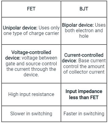
The difference between FET and BJT is explained in the following table:

Hence, Option C is correct.

Test: FET Amplifier - 2 - Question 10

The most commonly used feedback arrangement in cascaded amplifier is:

Detailed Solution for Test: FET Amplifier - 2 - Question 10

Analysis:-

Voltage series feedback is the most commonly used feedback arrangement in cascaded amplifiers.

This configuration increases input resistance and decreases output resistance.

Benefit of high input impedance:

  • It provides good amplification to the input signal, otherwise, we get low voltage and that leads to low amplification.
  • It minimizes the loading effect on input and a thus significant amount of input voltage signal is maintained for amplification.
Test: FET Amplifier - 2 - Question 11

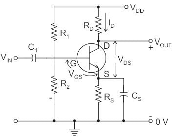
In a Common Drain (CD) MOSFET amplifier with voltage divider bias with R1 and R2 equal to 1.5 MΩ and 1 MΩ respectively, the input impedance Zf is:

Detailed Solution for Test: FET Amplifier - 2 - Question 11

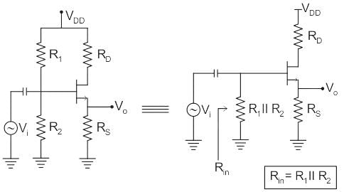
Common drain Amplifies with voltage divider bias and its small-signal equivalent circuit is as shown below:

Calculation:

Given:

R1 = 1.5 MΩ, R2 = 1 MΩ

So,

Rin = R1 ⋅ R2 / R1 + R2

Rin = 1.5MΩ × 1MΩ / 2.5MΩ

Rin = 600 kΩ

Test: FET Amplifier - 2 - Question 12

When a 1 V increase in the gate voltage changes the drain current 10 mA in a FET, its gm equals.

Detailed Solution for Test: FET Amplifier - 2 - Question 12

Concept:

Transconductance indicates the amount of control the gate has on the drain current.

Mathematically, the transconductance (gm) is defined as:

It is given the name transconductance because it gives the relationship between the input voltage and the output current.

Calculation:

Given: Δ VGS = 1 V and Δ ID = 10 mA

∴ 

= 0.01 mho

Test: FET Amplifier - 2 - Question 13

A common gate amplifier has

Detailed Solution for Test: FET Amplifier - 2 - Question 13

FET:

As the input circuit of FET is reverse biased, FET exhibits a much higher input impedance ( in the order of 100 M 12 ) and lower output impedance and there will be a high degree of isolation between input and output.

So, FET can act as an excellent buffer amplifier but the BJT has low input impedance because its input circuit is forward biased.

Test: FET Amplifier - 2 - Question 14

The bandwidth of an RC-coupled amplifier is limited by

Detailed Solution for Test: FET Amplifier - 2 - Question 14

(i) In capacitively coupled amplifiers, the coupling and bypass capacitors affect the low-frequency cut-off. These capacitors form a high-pass filter with circuit resistances.
(ii) Coupling and bypass capacitors are also called external capacitors.
For high-frequency response, it is determined by the device’s internal capacitance and the Miller effect.
(iii) Device internal capacitance is shunted and also called as Junction capacitors.

Test: FET Amplifier - 2 - Question 15

The common source stage of a CMOS amplifier Provides:

Detailed Solution for Test: FET Amplifier - 2 - Question 15

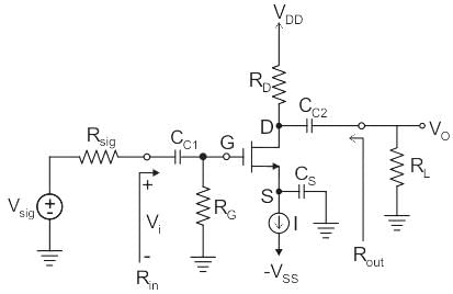
The value of Gate resistance (RG) is in mega-ohm (MΩ).

As Rin = RG

The input impedance of a common source amplifier is very high.

The value of ro, RD, and Rlies in kilo-ohm (kΩ). So the parallel combination of ro, RD, and Ris in kilo-ohm (kΩ). That’s why the output impedance and voltage gain of the common source amplifier is moderately high.

Information about Test: FET Amplifier - 2 Page
In this test you can find the Exam questions for Test: FET Amplifier - 2 solved & explained in the simplest way possible. Besides giving Questions and answers for Test: FET Amplifier - 2, EduRev gives you an ample number of Online tests for practice

Top Courses for Electrical Engineering (EE)

Download as PDF

Top Courses for Electrical Engineering (EE)