Electronics and Communication Engineering (ECE) Exam  >  Electronics and Communication Engineering (ECE) Tests  >  Test: Combinational Logic - Electronics and Communication Engineering (ECE) MCQ

Test: Combinational Logic - Electronics and Communication Engineering (ECE) MCQ


Test Description

10 Questions MCQ Test - Test: Combinational Logic

Test: Combinational Logic for Electronics and Communication Engineering (ECE) 2024 is part of Electronics and Communication Engineering (ECE) preparation. The Test: Combinational Logic questions and answers have been prepared according to the Electronics and Communication Engineering (ECE) exam syllabus.The Test: Combinational Logic MCQs are made for Electronics and Communication Engineering (ECE) 2024 Exam. Find important definitions, questions, notes, meanings, examples, exercises, MCQs and online tests for Test: Combinational Logic below.
Solutions of Test: Combinational Logic questions in English are available as part of our course for Electronics and Communication Engineering (ECE) & Test: Combinational Logic solutions in Hindi for Electronics and Communication Engineering (ECE) course. Download more important topics, notes, lectures and mock test series for Electronics and Communication Engineering (ECE) Exam by signing up for free. Attempt Test: Combinational Logic | 10 questions in 10 minutes | Mock test for Electronics and Communication Engineering (ECE) preparation | Free important questions MCQ to study for Electronics and Communication Engineering (ECE) Exam | Download free PDF with solutions
Test: Combinational Logic - Question 1

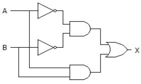
 Which of the following logic expressions represents the logic diagram shown?
Detailed Solution for Test: Combinational Logic - Question 1

1st output of AND gate is = A’B’
2nd AND gate’s output is = AB and,
OR gate’s output is = (A’B’)+(AB) = AB + A’B’.

Test: Combinational Logic - Question 2

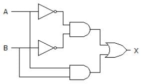
What type of logic circuit is represented by the figure shown below?
Detailed Solution for Test: Combinational Logic - Question 2

After solving the circuit we get (A’B’)+AB as output, which is XNOR operation. Thus, it will produce 1 when inputs are even number of 1s or all 0s, and produce 0 when input is odd number of 1s.

1 Crore+ students have signed up on EduRev. Have you? Download the App
Test: Combinational Logic - Question 3

Which of the following combinations of logic gates can decode binary 1101?

Detailed Solution for Test: Combinational Logic - Question 3

For decoding any number output must be high for that code and this is possible in One 4-input NAND gate, one inverter option only. A decoder is a combinational circuit that converts binary data to n-coded data upto 2n outputs.

Test: Combinational Logic - Question 4

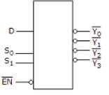
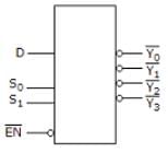
For the device shown here, assume the D input is LOW, both S inputs are LOW and the input is LOW. What is the status of the Y’ outputs?
Detailed Solution for Test: Combinational Logic - Question 4

In the given diagram, S0 and S1 are selection bits. So,
I/P S0 S1 O/P
D = 0 0 0 Y0
D = 0 0 1 Y1
D = 0 1 0 Y2
D = 0 1 1 Y3
Hence, inputs are S0 and S1 are Low means 0, so output is Y0 and rest all are HIGH.

Test: Combinational Logic - Question 5

3 bits full adder contains ________

Detailed Solution for Test: Combinational Logic - Question 5

Full Adder is a combinational circuit with 3 input bits and 2 output bits CARRY and SUM. Three bits full adder requires 23 = 8 combinational circuits.

Test: Combinational Logic - Question 6

The device shown here is most likely a ________

Detailed Solution for Test: Combinational Logic - Question 6

The given diagram is demultiplexer, because it takes single input & gives many outputs. A demultiplexer is a combinational circuit that takes a single output and latches it to multiple outputs depending on the select lines.

Test: Combinational Logic - Question 7

For a two-input XNOR gate, with the input waveforms as shown below, which output waveform is correct?

Detailed Solution for Test: Combinational Logic - Question 7

When both inputs are same then the o/p is high for a XNOR gate.
i.e., A B O/P
0 0 1
0 1 0
1 0 0
1 1 1.
Thus, it will produce 1 when inputs are even number of 1s or all 0s, and produce 0 when input is odd number of 1s.

Test: Combinational Logic - Question 8

Which of the following circuit has its output dependent only upon the present input?

Detailed Solution for Test: Combinational Logic - Question 8

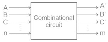
Combinational Logic circuits are circuits for which the present output depends only on the present input, i.e. there is no memory element to store the past output.

A combinational circuit can have ‘n’ number of inputs and ‘m’ number of outputs as shown:

Test: Combinational Logic - Question 9

Code conversion circuits mostly uses

Detailed Solution for Test: Combinational Logic - Question 9

Code conversion circuits are used to convert a digital code from one format to another. For example, a binary code can be converted to a Gray code, or a BCD (binary-coded decimal) code can be converted to a binary code. These circuits typically use a combination of logic gates, such as AND gates, OR gates, and XOR gates, to perform the necessary conversions.

However, the most commonly used type of circuit for code conversion is the AND-OR gate circuit. This circuit is based on a combination of AND gates and OR gates, and it can be used to implement various types of code conversion, such as binary to Gray code conversion and BCD to binary conversion. The AND-OR gate circuit is preferred for code conversion because it is simple, efficient, and provides a high level of flexibility.

Test: Combinational Logic - Question 10

Designing combinational circuit involves

Detailed Solution for Test: Combinational Logic - Question 10

Designing a combinational circuit typically involves 4 steps:

  1. Problem specification: This involves identifying the problem that the circuit needs to solve, and defining the input and output requirements.

  2. Truth table creation: This involves creating a truth table that shows the desired output for each possible combination of input values.

  3. Boolean expression derivation: This involves deriving a Boolean expression or set of expressions that represent the desired output in terms of the input variables.

  4. Logic diagram implementation: This involves implementing the Boolean expressions using logic gates, such as AND, OR, NOT, XOR, etc.

These 4 steps provide a systematic approach to designing combinational circuits that can be used for a wide range of problems. However, the number of steps required may vary depending on the complexity of the problem and the circuit being designed.

Information about Test: Combinational Logic Page
In this test you can find the Exam questions for Test: Combinational Logic solved & explained in the simplest way possible. Besides giving Questions and answers for Test: Combinational Logic, EduRev gives you an ample number of Online tests for practice

Top Courses for Electronics and Communication Engineering (ECE)

Download as PDF

Top Courses for Electronics and Communication Engineering (ECE)