Electronics and Communication Engineering (ECE) Exam  >  Electronics and Communication Engineering (ECE) Tests  >  Test: Extrinsic Semiconductors - Electronics and Communication Engineering (ECE) MCQ

Test: Extrinsic Semiconductors - Electronics and Communication Engineering (ECE) MCQ


Test Description

10 Questions MCQ Test - Test: Extrinsic Semiconductors

Test: Extrinsic Semiconductors for Electronics and Communication Engineering (ECE) 2024 is part of Electronics and Communication Engineering (ECE) preparation. The Test: Extrinsic Semiconductors questions and answers have been prepared according to the Electronics and Communication Engineering (ECE) exam syllabus.The Test: Extrinsic Semiconductors MCQs are made for Electronics and Communication Engineering (ECE) 2024 Exam. Find important definitions, questions, notes, meanings, examples, exercises, MCQs and online tests for Test: Extrinsic Semiconductors below.
Solutions of Test: Extrinsic Semiconductors questions in English are available as part of our course for Electronics and Communication Engineering (ECE) & Test: Extrinsic Semiconductors solutions in Hindi for Electronics and Communication Engineering (ECE) course. Download more important topics, notes, lectures and mock test series for Electronics and Communication Engineering (ECE) Exam by signing up for free. Attempt Test: Extrinsic Semiconductors | 10 questions in 30 minutes | Mock test for Electronics and Communication Engineering (ECE) preparation | Free important questions MCQ to study for Electronics and Communication Engineering (ECE) Exam | Download free PDF with solutions
Test: Extrinsic Semiconductors - Question 1

Which of the following statement is correct?

Detailed Solution for Test: Extrinsic Semiconductors - Question 1
  • Semiconductors possess specific electrical properties.
  • A substance that conducts electricity is called a conductor, and a substance that does not conduct electricity is called an insulator.
  • Semiconductors are substances with properties somewhere between them.

n-type semiconductor:

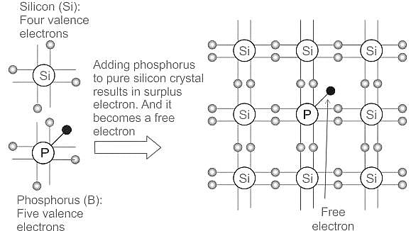
  • An n-type semiconductor is an intrinsic semiconductor doped with Phosphorus (P), arsenic (As), or antimony (Sb) as an impurity.
  • Silicon of Group IV has four valence electrons and phosphorus of Group V has five valence electrons.
  • If a small amount of phosphorus is added to a pure silicon crystal, one of the valence electrons of phosphorus becomes free to move around as a surplus electron.
  • When this free electron is attracted to the “+” electrode and moves, current flows.


P-type semiconductor:

  • A p-type semiconductor is an intrinsic semiconductor doped with boron (B) or indium (In).
  • Silicon of Group IV has four valence electrons and boron of Group III has three valence electrons.
  • If a small amount of boron is doped to a single crystal of silicon, valence electrons will be insufficient at one position to bond silicon and boron, resulting in holes that lack electrons.
  • When a voltage is applied in this state, the neighboring electrons move to the hole, so that the place where an electron was present becomes a new hole, and the holes appear to move to the "–" electrode in sequence.

  • A p-type semiconductor is created by doping an intrinsic semiconductor with an acceptor impurity.
  • ​An n-type semiconductor is created by doping an intrinsic semiconductor with a donor impurity
Test: Extrinsic Semiconductors - Question 2

When Si is doped with ________ an n-type semiconductor is formed.

Detailed Solution for Test: Extrinsic Semiconductors - Question 2
  • An n-type semiconductor is an intrinsic semiconductor doped with phosphorus (P), arsenic (As), or antimony (Sb) as an impurity.
  • Silicon of Group IV has four valence electrons and phosphorus of Group V has five valence electrons.
  • If a small amount of phosphorus is added to a pure silicon crystal, one of the valence electrons of phosphorus becomes free to move around as a surplus electron.
  • When this free electron is attracted to the “+” electrode and moves, current flows.

  • When Si is doped with Phosphorus an n-type semiconductor is formed.
  • When Si is doped with Boron, indium an p-type semiconductor is formed.
1 Crore+ students have signed up on EduRev. Have you? Download the App
Test: Extrinsic Semiconductors - Question 3

Two statements are given-one labelled Assertion (A) and the other labelled Reason (R). Select the correct answer to these questions from the codes (a), (b), (c) and (d) as given below.
ASSERTION(A): The electrical conductivity of a semiconductor increases on doping.
REASON: Doping always increases the number of electrons in the semiconductor. 

Detailed Solution for Test: Extrinsic Semiconductors - Question 3
  • Semiconductors are the materials that have conductivity between conductors and insulators.
  • There are two types of semiconductors : Intrinsic and Extrinsic semiconductors.
  • Intrinsic semiconductors are pure semiconductors which is made up of only single element like germanium or silicon.
  • The conductivity of semiconductors can be improved by adding impurities. The process of adding impurities to a pure semiconductor is called doping.
  • Extrinsic semiconductors are the semiconductors that are doped with specific impurities to modify the electrical properties.
    • It is further classified into n-type and p-type.
    • n-type semiconductors are doped with pentavalent impurities or atoms such as Phosphorus or Arsenic then four out of five bond with Germanium or Silicon and the last one is free electron which is responsible for conduction in n-type.
    • p-type semiconductors are doped with trivalent impurities or atoms such as Aluminium or Boron then three electrons will bond with Germanium or Silicon and one hole will be left which is responsible for conduction in p-type.
    • Thus on doping the electrical conductivity of semiconductor increases. Thus Assertion is True
  • ​Doping of pentavalent atoms increases the number of electrons but doping of trivalent atoms will increase the number of holes. Thus, Reason is False.

​Hence, the correct option is (3)

Test: Extrinsic Semiconductors - Question 4

A semiconductor is doped with phosphorous atoms as impurity. The impurity levels created in the semiconductor are close to the

Detailed Solution for Test: Extrinsic Semiconductors - Question 4
  • N-type semiconductor: An extrinsic semiconductor where the dopant atoms provide extra conduction electrons to the host material like Phosphorus(P) in Silicon (Si) called donor impurities.
  • For an n-type semiconductor, there are more electrons in the conduction band than there are holes in the valence band.
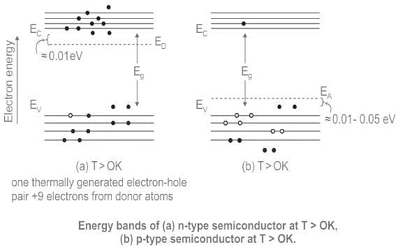
  • This leads to formation of donor energy level below conduction band in forbidden energy gap, which implies that the probability of finding an electron near the conduction band edge is larger than the probability of finding a hole at the valence band edge.

Hence, the correct option is (2)

Test: Extrinsic Semiconductors - Question 5

n-type semiconductor is:

Detailed Solution for Test: Extrinsic Semiconductors - Question 5

Semiconductor: A solid substance that has a conductivity between an insulator and metals.

  • Semiconductors have conductivity due to many factors like the addition of an impurity or because of temperature effects.

N-type semiconductors: An extrinsic semiconductor where the dopant atoms provide extra conduction electrons to the host material like Phosphorus P in Silicon Si.

  • This creates an excess of negative (n-type) electron charge carriers that are able to move freely.

P-type semiconductors: A semiconductor, when the impurity with trivalency is added to pure semiconductors, then it is known as a p-type semiconductor.

  • Impurities with trivalency such as Boron (B), Gallium (Ga), Indium(In), Aluminium(Al), etc are called acceptor impurity.

  • P-type and N-type materials are NOT positively and negatively charged. 
    • because atoms are electrically neutral.
  • ​N-type materials have electrons or negative charges that are majority carriers and holes are minority carriers. 
  • So it has mainly electrons or negative charge carriers that can move freely, but it is still neutral because the fixed donor atoms, having donated electrons, are positive.
  • Thus we can say that the n-type of semiconductor is neutral.

Hence option 2 is correct.

Test: Extrinsic Semiconductors - Question 6

To obtain electrons as majority charge carriers in a semiconductor the impurity mixed is:

Detailed Solution for Test: Extrinsic Semiconductors - Question 6
  • The material which is not a good conductor or a good insulator is called a semiconductor.
  • For example Silicon
  • The charge carriers which are present in more quantity in a semiconductor compared to other particles are called the majority charge carrier.
  • ​Extrinsic semiconductors are of two types
    • ​N-type Semiconductor
    • P-type Semiconductor

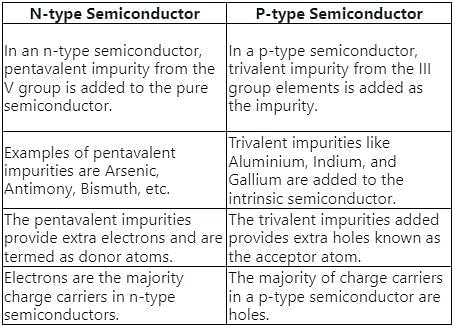
  • ​In an n-type semiconductor, pentavalent impurity from the V group is added to the pure semiconductor.
  • Electrons are the majority charge carriers in n-type semiconductors.

Hence, option 4 is correct.

Test: Extrinsic Semiconductors - Question 7

Which of the following statement is False?

Detailed Solution for Test: Extrinsic Semiconductors - Question 7
  • A P-type semiconductor is formed when a tetravalent impurity(Si, Ge) is doped with a trivalent impurity(B, Ga)
  • Holes are the majority charge carriers  and electrons are minority charge carriers in P-type semiconductors
  • An n-type Semiconductor is formed when a tetravalent impurity(Si, Ge) is doped with a Pentavalent impurity(P,Sb)
  • Electrons are the majority charge carriers in the n-type semiconductor and holes are minority charge carriers. 

  • A pure semiconductor is called an intrinsic semiconductor. It has thermally generated current carriers.
  • As temperature increases, more and more hole, and electron pairs are generated and after a certain temperature and it will behave as ideal conductors. Thus the resistance of intrinsic semiconductor decreases with the increase of temperature. Therefore option1 is correct.
  • When a pure Si crystal is doped with trivalent impurities, then a p-type semiconductor is formed. Therefore option 2 is correct.
  • From above it is clear that electrons are the majority charge carriers in an n-type semiconductor. Therefore option 3 is incorrect.
  • From above it is clear that holes are the majority charge carriers in a P-type Semiconductor. Therefore option 4 is correct.
Test: Extrinsic Semiconductors - Question 8

What is the difference between intrinsic semiconductor and extrinsic semiconductor?

Detailed Solution for Test: Extrinsic Semiconductors - Question 8

Intrinsic Semiconductor: The intrinsic semiconductor is a pure semiconductor.

  • Since they are pure semiconductors they have the same number of holes and electrons.
  • The conductivity of an intrinsic semiconductor is very low at room temperature.

Extrinsic Semiconductor: We add a small amount of impurity to the pure semiconductor.

  • This increases the conductivity of the semiconductor by manifold.
  • This impure semiconductor is called an extrinsic semiconductor.

Option 1: The conductivity of an intrinsic semiconductor is very low at room temperature. It means very low or no current flows at room temperature.

  • So this is an incorrect statement.

Option 2: Since intrinsic semiconductors are pure semiconductors they have the same number of holes and electrons. 
Option 3 and 4: The intrinsic semiconductor is a pure semiconductor and an extrinsic semiconductor is a semiconductor with impurity.

  • So option 4 gives the correct statement.

So the correct answer is option 4.

Test: Extrinsic Semiconductors - Question 9

Pick statement that is correct for a p-type semi-conductor:

Detailed Solution for Test: Extrinsic Semiconductors - Question 9
  • Holes are the majority charge carriers in p-type semiconductors. Therefore the overall charge of the material is positive.
  • In a p-type semiconductor, trivalent impurity from the III group elements is added as the impurity.

Hence, option 2 is correct.

Test: Extrinsic Semiconductors - Question 10

The Fermi level for an extrinsic ‘n’ type semiconductor:

Detailed Solution for Test: Extrinsic Semiconductors - Question 10

Fermi level in a semiconductor: It is that energy level in the energy-band-diagram of semiconductor for which the probability of occupancy (i.e., the presence of main current carriers electrons or holes) becomes half. 

From the above diagram, it is clear that the Fermi level is close to the conduction band edge.

  • As Temperature increases then the fermi level moves towards the centre of forbidden gap irrespective of whether it is p-type or n-type.
    • For n-type material as the doping increases then fermi level moves towards the conduction band.
    • For p-type material as the doping increases then fermi level moves towards the valence band.
  • If doping is very large, then the Fermi level may move into the conduction band.
     
Information about Test: Extrinsic Semiconductors Page
In this test you can find the Exam questions for Test: Extrinsic Semiconductors solved & explained in the simplest way possible. Besides giving Questions and answers for Test: Extrinsic Semiconductors, EduRev gives you an ample number of Online tests for practice

Top Courses for Electronics and Communication Engineering (ECE)

Download as PDF

Top Courses for Electronics and Communication Engineering (ECE)