MPPGCL JE Electronics Mock Test - 1 Free Online Test 2026
Full Mock Test & Solutions: MPPGCL JE Electronics Mock Test - 1 (100 Questions)
You can boost your Electronics and Communication Engineering (ECE) 2026 exam preparation with this MPPGCL JE Electronics Mock Test - 1 (available with detailed solutions).. This mock test has been designed with the analysis of important topics, recent trends of the exam, and previous year questions of the last 3-years. All the questions have been designed to mirror the official pattern of Electronics and Communication Engineering (ECE) 2026 exam, helping you build speed, accuracy as per the actual exam.
Mock Test Highlights:
- - Format: Multiple Choice Questions (MCQ)
- - Duration: 120 minutes
- - Total Questions: 100
- - Analysis: Detailed Solutions & Performance Insights
- - Sections covered: Electronics, General Awareness and Aptitude
Sign up on EduRev for free and get access to these mock tests, get your All India Rank, and identify your weak areas to improve your marks & rank in the actual exam.

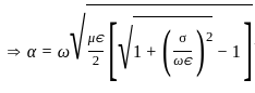
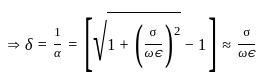
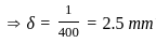
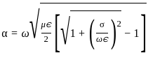
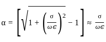
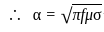
The attenuation constant of a medium is 400/m. Find the skin depth in the medium.
Detailed Solution: Question 1


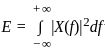
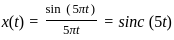
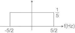
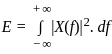
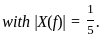
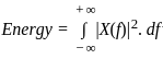
Consider the signal 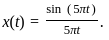 The energy of the signal is
The energy of the signal isDetailed Solution: Question 2
 .
.

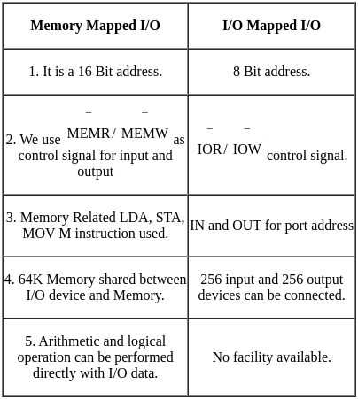
In a 8085 microprocessor system with memory mapped I/O
Detailed Solution: Question 3
Shifting the register content to left by two bits can be used to implement
Detailed Solution: Question 4
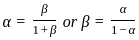
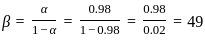
If α = 0.98, Ico = 6 μA, & IB = 100 μA for a transistor, then the value of IC will be
Detailed Solution: Question 5
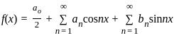
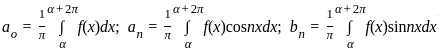
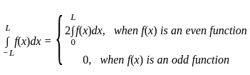
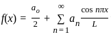
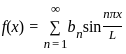
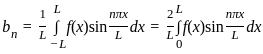
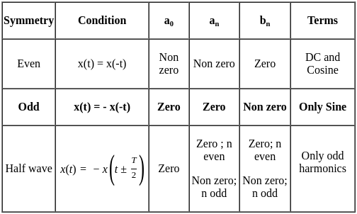
Fourier series of an odd periodic function contains only
Detailed Solution: Question 6
What is the maximum data rate that can be transmitted using a QPSK modulation with a roll-off factor of 0.2 for a 36 MHz transponder?
Detailed Solution: Question 7


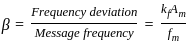
In a frequency modulated (FM) system, when the audio frequency is 500 Hz and the audio frequency voltage is 2.4 V, the frequency deviation δ is 4.8 kHz. If the audio frequency voltage is now increased to 7.2 V then what is the new value of deviation?
Detailed Solution: Question 8


Which of the following is NOT a cursor control devices used in CAD systems
Detailed Solution: Question 9
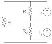
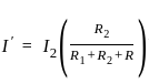
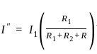
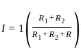
In the given circuit, if R1 = R2 = R = 1 Ω and I1 = I2 = 1 A. Then current through Resistor R is:
Detailed Solution: Question 10


Tuning of VCO frequency with the input frequency by the loop in Phase locked loop is known as:
Detailed Solution: Question 11
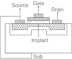
In an n-MOS transistor, when Vgs = 0, and to cause the existing channel to cease to exist, a negative voltage Vtd (threshold Voltage) must be applied between gate and source. The transistor operates in:
Detailed Solution: Question 12
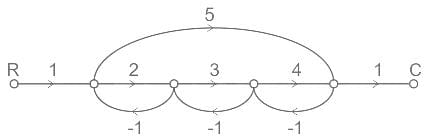
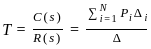
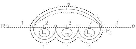
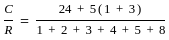
In the signal flow graph of figure given below, the gain C/R will be
Detailed Solution: Question 13

Which of the following PCM schemes is depicted in the below figure?
Detailed Solution: Question 14
What will be the decimal equivalent for binary number 11010011?
Detailed Solution: Question 15
The electric field due to a point charge at distance ‘r’ is
Detailed Solution: Question 16

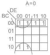
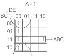
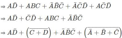
Simplify the below function represented in sum of minterms
F(A, B, C, D, E) = ∑ (0, 1, 2, 3, 8, 9, 16, 17, 20, 21, 24, 25, 28, 29, 30, 31)
Detailed Solution: Question 17
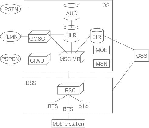
The GSM system architecture consists of the following major interconnected subsystem(s).
Detailed Solution: Question 18
The total number of complex multiplications required for a 32- point FFT (Fast Fourier Transform) is:
Detailed Solution: Question 19

 = 16 × 5 = 80
An IP packet has arrived with the first 8 bits as 0100 0010. Which of the following is correct?
Detailed Solution: Question 20
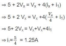
Determine the current 'i1' in the circuit of figure shown below -
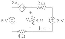
Detailed Solution: Question 21

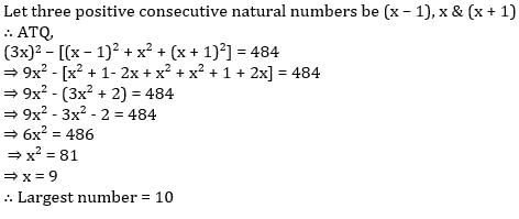
If the square of sum of three positive consecutive natural numbers exceeds the sum of their corresponding squares by 484 then what is the largest of the three numbers?
Detailed Solution: Question 22
In this questions, a number series is given with one term missing. Choose the correct alternative that will continue the same pattern and fill in the black spaces.
Q. 3, 9, 27, 81, (____)
Detailed Solution: Question 23
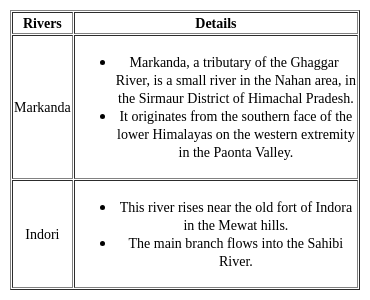
Sahibi river originates in which of the following districts?
Detailed Solution: Question 24
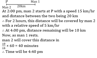
A man starts running from point P at 11:00 a.m. with a speed of 10 km/hr. He runs for 2 hours and then takes a 1 hour rest. He continues the pattern till he is caught by another man who starts at 2:00 p.m. from point P and runs non-stop at a speed of 15 km/hr towards the first man. At what time (in p.m.) will the first man be caught?
Detailed Solution: Question 25
Choose the alternative which is an odd word/number/letter pair out of the given alternatives.
Detailed Solution: Question 26
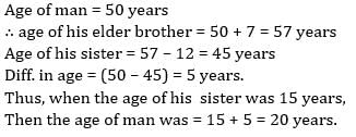
A man is 50 years old. His brother is 7 years older than him and his sister is 12 years younger than his brother. When his sister was 15 years old, then the men’s age was :
Detailed Solution: Question 27
The combined amount spent on 30 books and 120 notebooks is Rs. 15,000. If the price of each book is Rs. 400, what is the price of each notebook?
Detailed Solution: Question 28

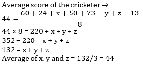
The average score of a cricketer in 8 innings is 44. He had scored 60, 24, x, 50, 73, y, z, 13 respectively in those innings. Find the average of x, y and z?
Detailed Solution: Question 29
Detailed Solution: Question 30