Electronics and Communication Engineering (ECE) Exam  >  Electronics and Communication Engineering (ECE) Tests  >  MPPGCL JE Electronics Mock Test - 2 - Electronics and Communication Engineering (ECE) MCQ

MPPGCL JE Electronics Mock Test - 2 - Electronics and Communication Engineering (ECE) MCQ


Test Description

30 Questions MCQ Test - MPPGCL JE Electronics Mock Test - 2

MPPGCL JE Electronics Mock Test - 2 for Electronics and Communication Engineering (ECE) 2024 is part of Electronics and Communication Engineering (ECE) preparation. The MPPGCL JE Electronics Mock Test - 2 questions and answers have been prepared according to the Electronics and Communication Engineering (ECE) exam syllabus.The MPPGCL JE Electronics Mock Test - 2 MCQs are made for Electronics and Communication Engineering (ECE) 2024 Exam. Find important definitions, questions, notes, meanings, examples, exercises, MCQs and online tests for MPPGCL JE Electronics Mock Test - 2 below.
Solutions of MPPGCL JE Electronics Mock Test - 2 questions in English are available as part of our course for Electronics and Communication Engineering (ECE) & MPPGCL JE Electronics Mock Test - 2 solutions in Hindi for Electronics and Communication Engineering (ECE) course. Download more important topics, notes, lectures and mock test series for Electronics and Communication Engineering (ECE) Exam by signing up for free. Attempt MPPGCL JE Electronics Mock Test - 2 | 100 questions in 120 minutes | Mock test for Electronics and Communication Engineering (ECE) preparation | Free important questions MCQ to study for Electronics and Communication Engineering (ECE) Exam | Download free PDF with solutions
MPPGCL JE Electronics Mock Test - 2 - Question 1

Which among the given statement is/are CORRECT?

(a) Avalanche breakdown voltage increases with temperature

(b) Zener breakdown voltage decreases with temperature

Detailed Solution for MPPGCL JE Electronics Mock Test - 2 - Question 1

Avalanche breakdown and temperature effect:

  • In avalanche breakdown, a bunch of electrons knocks out another electron to conduction band creating electron-hole pair.
  • Due to an increase in temperature, vibrations, of atoms increases and thus reduces the mean free path for electrons.
  • Hence in avalanche breakdown voltage increases with temperature.

Hence it is a positive temperature coefficient.

Zener breakdown and temperature effect:

  • It occurs when the electric field is much stronger to move the electrons from the valence band to the conduction band.
  • As temperature increases, bandgap decreases so less electric field is required to
  • Hence Zener breakdown voltage decreases as the temperature increases. Thus it has a negative temp coefficient.
MPPGCL JE Electronics Mock Test - 2 - Question 2

In ASK modulation:

Detailed Solution for MPPGCL JE Electronics Mock Test - 2 - Question 2

Digital Modulation Techniques:

1) Amplitude shift key

2) Frequency shift key

3) Phase Shift key

4) QAM

ASK System:

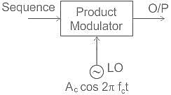
1. In the ASK modulation scheme, a finite number of amplitudes are used for binary 1 and 0 transmission.

2. For ASK Transmitter on-off keying is used.

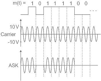
3. In Amplitude Shift Keying (ASK) binary 1 is represented with the presence of carrier and binary 0 is represented with the absence of the carrier.

1 : s1(t) = Ac cos 2πfct

0 : s2 (t) = 0

Hence,

ASK = [± 10 V, 0, ± 10 V, ± 10 V, ± 10 V, ± 10 V, 0, 0]

Important Point

FSK (Frequency Shift Keying):

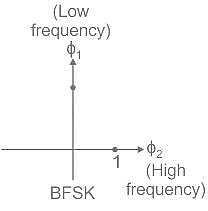
In FSK (Frequency Shift Keying) binary 1 is represented with a high-frequency carrier signal and binary 0 is represented with a low-frequency carrier, i.e. In FSK, the carrier frequency is switched between 2 extremes.

For binary ‘1’ → S1 (A) = Acos 2π fHt

For binary ‘0’ → S2 (t) = A cos 2π fLt . The constellation diagram is as shown:

PSK(Phase Shift Keying):

In PSK (phase shift keying) binary 1 is represented with a carrier signal and binary O is represented with 180° phase shift of a carrier

For binary ‘1’ → S1 (A) = Acos 2π fct

For binary ‘0’ → S2 (t) = A cos (2πfct + 180°) = - A cos 2π fct

The Constellation Diagram Representation is as shown:

1 Crore+ students have signed up on EduRev. Have you? Download the App
MPPGCL JE Electronics Mock Test - 2 - Question 3

A bandpass signal occupies the bandwidth 390 kHz to 410 kHz. What minimum sampling frequency would you use from the options given below, so as to avoid aliasing?

Detailed Solution for MPPGCL JE Electronics Mock Test - 2 - Question 3

Concept:

The sampling frequency of the bandpass signal is given by:

Where

  (Where [ .] denotes the floor value)

Analysis:

Given:

fL = 390 kHz, fH = 410 kHz

fs ≈ 41 kHz 

MPPGCL JE Electronics Mock Test - 2 - Question 4

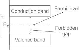
The valence band and conduction band for a semiconductor are:

Detailed Solution for MPPGCL JE Electronics Mock Test - 2 - Question 4

CONCEPT:

Fermi level: 

  • The highest energy level that an electron can occupy at the absolute zero temperature is known as the Fermi Level.
  • The Fermi level lies between the valence band and conduction band because at absolute zero temperature the electrons are all in the lowest energy state. Due to a lack of sufficient energy at 0 Kelvin, the Fermi level can be considered as the sea of fermions (or electrons) above which no electrons exist.

Hence the valence band and conduction band for a semiconductor are nearer to the fermi level.

MPPGCL JE Electronics Mock Test - 2 - Question 5

If a filter has 60 dB bandwidth of 10 kHz and 3 dB bandwidth of 4 kHz, the shape factor will be _______.

Detailed Solution for MPPGCL JE Electronics Mock Test - 2 - Question 5

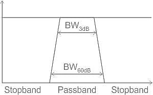
The transition band characteristics we are usually interested in deal with the shape or steepness of the roll-off between the passband and the stopband. Usually, the shape factor is defined as shown in Figure (which shows an otherwise ideal filter with just the addition of transition bands). It is defined for two levels of attenuation and is usually taken to be the ratio between 3dB of attenuation (passband) and given stopband attenuation.

For example, we could take 3dB to define the passband and 60dB to use the stopband.

Our ideal filter would have a shape factor of unity, but where this is not physically realizable we seek the smallest shape factor we can. For reference, simple RLC filters might have shape factors in the range of ~3, SAW filters in the range of ~1.5.

     ---(1)

Calculation:

Given:

BW at 60 dB = 10 kHz

BW at 3 dB = 4 kHz

From equation (1)

MPPGCL JE Electronics Mock Test - 2 - Question 6

A second order control system is NOT required to satisfy the following specification:
Detailed Solution for MPPGCL JE Electronics Mock Test - 2 - Question 6

Concept:

Time-domain specification (or) transient response parameters:

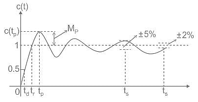
Peak Time (tp):

It is the time taken by the response to reach the maximum value.

Settling time (Ts):

It is the time taken by the response to reach ± 2% tolerance band as shown in the fig above.

  for a 5% tolerance band.

 for 2% tolerance band

If ξ increases, rise time, peak time increases and peak overshoot decreases.

Delay time

The time taken by a response to rising from 0 to 50% of the final value is known as ‘delay time’.

Peak overshoot is the maximum error at the output.

Peak overshoot, 

% peak overshoot,


Important Points

  • A practical second-order system should be required to meet all the specifications mentioned above.
  • If it is an underdamped system, the system needs to satisfy the overshot to a given step input.
  • Settling time is another specification that needs to be as less as possible so that the system will reach a steady-state in less time.
  • Steady-state accuracy gives, how close the output of the system is to the required output.
  • But, variations in step output are not a required specification for a second-order system.
MPPGCL JE Electronics Mock Test - 2 - Question 7

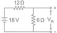
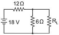
In the circuit shown above, the maximum power absorbed by the load resistance RL is

Detailed Solution for MPPGCL JE Electronics Mock Test - 2 - Question 7

Concept:

Maximum power transfer theorem:

Maximum power transfer theorem states that " In a linear bilateral network if the entire network is represented by its Thevenin's equivalent circuit then the maximum power transferred from source to the load when the load impedance is equal to the complex conjugate of  Thevenin's impedance".

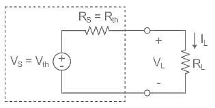
Let's consider variable resistive load and Thevenin's equivalent network as shown below,


Apply KVL, for the above circuit

Vth - ILRth - ILRL = 0

Where

Vth is the source or Thevenin's voltage, IL is the load current, RL is the load resistance, Rth is the source or Thevenin's resistance

Vth = IL (Rth + RL)

IL = Vth / (Rth + RL)

P = ILRL

P = 

For maximum power transfer, RL = RS

Then the maximum power transferred is given by

Calculation:

To find Vth:

By applying the voltage division rule, we get

Vth = (18 × 6) / (12 + 6) 

⇒ Vth = 6 V

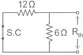
To find Rth:

From the above circuit,

Rth = 12 // 6 = (12 × 6) / (12 + 6) 

⇒ Rth = 4 Ω 

Then the maximum power transferred is given by

⇒ Pmax = (6)2 / 4 × 4 = 2.25 W

MPPGCL JE Electronics Mock Test - 2 - Question 8
A pulsed radar, operating at 3 GHz, having a pulse width of 2 μsec receives an echo from a target, 10 μsec after sending the signal. The approximate range of the target is
Detailed Solution for MPPGCL JE Electronics Mock Test - 2 - Question 8

Concept:

In the RADAR system, the range of the target is:


And,

PRT = (PW + RT) μ sec

Where

C = 3 × 10⁸ m/s = speed of light at which EMW travel

PRT = Pulse repetition time

PW = Pulse width

RT = rest time i.e. time interval between sending a pulse and return from target to the receiver.

Calculation:

Given that,

PW = 2 μ sec

RT = 10 μ sec

PRT = 2 + 10 = 12 μ sec


If we take an approximate value of PRT, we can write:

PRT = 2 + 10 10 μ sec


MPPGCL JE Electronics Mock Test - 2 - Question 9

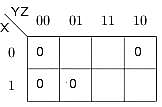
A boolean function is given as F(x, y, z) = ∑(1, 3, 6, 7). What is its equivalent canonical form?

Detailed Solution for MPPGCL JE Electronics Mock Test - 2 - Question 9

Concept:

Min Terms: 

  • A minterm is a boolean expression written for all those terms whose value is 1 in the K-map.
  • It is denoted by: F(x, y, z) = ∑(minterms)

MaxTerms: 

  • A maxterm is a boolean expression written for all those terms whose value is 0 in the K-map.
  • It is denoted by: F(x, y, z) = π(max terms)
  • Max terms are the compliments of minterms.

Explanation:

Given,  F(x, y, z) = ∑(1, 3, 6, 7)

Binary representation is:

 F(x, y, z) = ∑(001, 011, 010, 011)

It is minterm representation.

F(x, y, z) = ∑(000, 010, 100, 101)

F(x, y, z) = ∏ (0, 2, 4, 5)

It is max max-term representation.

MPPGCL JE Electronics Mock Test - 2 - Question 10
In RADAR, a low detection threshold is undesirable because _____
Detailed Solution for MPPGCL JE Electronics Mock Test - 2 - Question 10

1) When the unwanted thermal noise exceeds the present threshold level, then false alarms are generated.

2) If the threshold is set too low, the large number of false alarms will mask the detection of valid targets. 

3) If the threshold is set too higher there will be very few false alarms, but it can inhibit the detection of valid targets.

4) One solution for the false-alarm problem is the implementation of a constant false alarm rate that varies the detection threshold based on the environment.
MPPGCL JE Electronics Mock Test - 2 - Question 11
Maxwell's third equation is derived from _______.
Detailed Solution for MPPGCL JE Electronics Mock Test - 2 - Question 11

EXPLANATION:

Faraday’s Law states that a change in magnetic flux induces an emf in a coil.

Also, Lenz’s Law states that this induced emf produces a flux which opposes the flux that generates this emf, i.e.

     ----(1)

EMF is also defined as:

Also, 

Putting the above in Equation (1), we get:

Additional Information

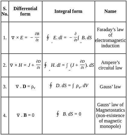
Maxwell's Equations for time-varying fields is as shown:

MPPGCL JE Electronics Mock Test - 2 - Question 12

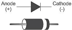
When a diode is given an external voltage that increases its potential barrier and restricts the flow of current, then it is called?

Detailed Solution for MPPGCL JE Electronics Mock Test - 2 - Question 12

The correct answer is option 1):(Reversed biasing)

Concept:

Diode

A diode is a semiconductor device that essentially acts as a one-way switch for current.

It allows current to flow easily in one direction but severely restricts current from flowing in the opposite direction

The reverse bias of the diode

  • When an external voltage (V ) is applied across the diode such that the n-side is positive and the p-side is negative, it is said to be reverse-biased.
  • The applied voltage mostly drops across the depletion region. The direction of the applied voltage is the same as the direction of barrier potential.
  • As a result, the barrier height increases, and the depletion region widens due to the change in the electric field.
  • When a diode is given an external voltage that increases its potential barrier and restricts the flow of current.

Additional Information
Forward biased diode:

  • In the forward bias, the p side of the diode is connected to the positive side of the battery and the n side is connected to the negative side of the battery.
  • The direction of the applied voltage is opposite to the junction barrier potential. Therefore, the size of the depletion region decreases.
MPPGCL JE Electronics Mock Test - 2 - Question 13

Which of the following will be the value of Q

Detailed Solution for MPPGCL JE Electronics Mock Test - 2 - Question 13

The given circuit is redrawn as:

DIAGRAM

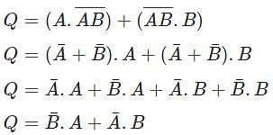
The output Q will be:

Applying De-Morgan's Law, the above expression becomes:

Q = A ⊕ B, i.e. A EXOR B

MPPGCL JE Electronics Mock Test - 2 - Question 14
Which of the following is a sequential access memory?
Detailed Solution for MPPGCL JE Electronics Mock Test - 2 - Question 14

The correct answer is Magnetic Tape.

  • Magnetic tape is a secondary storage device used for storing files of data; Example: a company’s payroll record.
  • Access is sequential and consists of records that can be accessed one after another as the tape moves along a stationary read-write mechanism
  • A hard disk is an electromechanical data storage device from which data is accessed in a random-access manner, individual blocks of data can be stored or retrieved in any order
  • Both sequential and random access of data is possible in hard disk
  • In random-access memory (RAM) the memory cells can be accessed for information transfer from any desired random location
  • That is, the process of locating a word in memory is the same and requires an equal amount of time no matter where the cells are located physically in memory; Hence RAM is random access
MPPGCL JE Electronics Mock Test - 2 - Question 15

An event has two possible outcomes with probability P1 =  and P1 = . The rate of information with 16 outcomes per second is -

Detailed Solution for MPPGCL JE Electronics Mock Test - 2 - Question 15

Concept:

Information associated with the event is “inversely” proportional to the probability of occurrence.

Entropy: The average amount of information is called the “Entropy”.

Rate of information = r.H

Calculation:

Given: r = 16 outcomes/sec

, and  

∴ Rate of information = r.H

R= 16 x 19/32

Rs = 19/2 or 38/4 bits/sec

MPPGCL JE Electronics Mock Test - 2 - Question 16

In the following, pick out the linear systems

(i) d2y(t)/dt2 + 9a1dy(t)/dt + a2y(t) = u(t)

(ii) y(t)dy(t)/dt + a1y(t) = a2 u(t)

(iii) 2d2y(t)/dt2 + tdy(t)/dt + t2y(t) = 5

Detailed Solution for MPPGCL JE Electronics Mock Test - 2 - Question 16

Concept:

A system is linear, if the operations on the input signal are all linear and no signal-independent terms are contained. Basic linear operations are given below-

  • Multiplication of input signal with a constant value: y(t) = ax(t)
  • Time-shifting the input signal y(t) = x(t−t1)
  • Scaling of the input signal y(t) = x(bt)
  • Combinations of scalling,shifting and multiplication , e.g. y(t) = ax(b(t−t1))
  • Summations of terms that are linear, e.g. y(t) = ax(t)+x(t−t1)
  • Convolution of two input signal, eg y(t) = x(t)*h(t)

Some non-linear operations are given below-

  • Multiplication of the signal with itself, i.e. y(t) = x(t)⋅x(t)
  • Applying any non-linear function to the signal, e.g. y(t) = sin(x(t))
  • Adding constant terms, which are independent of the signal, i.e. y(t) = x(t)+a

Analysis:

(I)  d2y(t)/dt2 + 9a1dy(t)/dt + a2y(t) = u(t) is linear

(ii) y(t) dy(t)/dt + a1y(t) = a2u(t) is non-linear due to multiplication of y(t)

(iii).  2d2y(t)/dt2 + dy(t)/dt + t2y(t) = 5 is Non Linear because of the contant term 5.

MPPGCL JE Electronics Mock Test - 2 - Question 17

Determine whether the following statements are true or false with respect to Pulse Amplitude Modulation. 

a) Instantaneous sampling of the message signal m(t) every Ts second, where the sampling rate fs = 1/Ts is chosen in accordance of the sampling theorem. 

b) Lengthening the duration of each sample obtained to some constant value T. 

Detailed Solution for MPPGCL JE Electronics Mock Test - 2 - Question 17

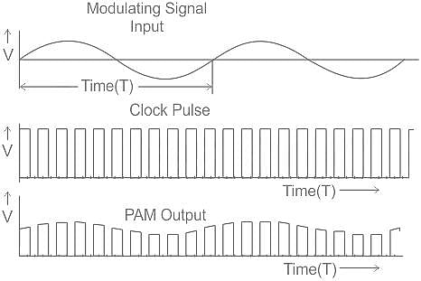
PAM (Pulse Amplitude Modulation)

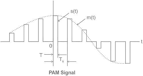
The width and location of pulses in a modulated signal (PAM) are constant, while the amplitude of pulses varies proportionally with the amplitude of an analogical useful signal.

The pulses in a PAM signal may of Flat-top type or natural type or ideal type.

Generation of PAM:

There are two operations involved in the generation of PAM signal:

  • Instantaneous sampling of the message signal m(t) every Ts seconds, where the sampling rate fs = 1/Ts is chosen in accordance with the sampling theorem. ('a' is True)
  • Lengthening the duration of each sample so obtained to some constant value T. ('b' is True)

MPPGCL JE Electronics Mock Test - 2 - Question 18
What will be the resistivity of an n-type Germanium sample at 300 K? The sample has a donor density of Nd = 1020 atoms/m3. Assume all donors to be ionized and take μn = 0.38 and q = 1.6 × 10⁻¹⁹ Coul.
Detailed Solution for MPPGCL JE Electronics Mock Test - 2 - Question 18

Concept:

In an extrinsic semiconductor, the conductivity (hence resistivity) depends on the number of carriers present and is given by:

n0 = majority carrier electron concentration

p0 = majority carrier hole concentrationμn and μp are the electron and hole mobilities respectively.

The resistivity is the inverse of conductivity, i.e.

Calculation:

Since the intrinsic carrier concentration of Germanium is of the order of 1013, and the given donor density is of the order of 1020, we can write:

n0 = Nd = 1020 atoms/m3

Since there is no acceptor impurity, p0 << n0 and can be easily neglected and the resistivity becomes:

ρ = 0.164 Ωm

MPPGCL JE Electronics Mock Test - 2 - Question 19
The filter which has ripple response in pass band and flat response in stop band is
Detailed Solution for MPPGCL JE Electronics Mock Test - 2 - Question 19

Chebyshev Filter:

  • It is also called an equal rip­ple filter.
  • It gives a sharper cut-off than Butterworth filter in the passband.
  • It has a ripple response in the passband and flat response in the stopband. it is also known as an equal-ripple response.
  • Both Butterworth and Chebyshev filters exhibit large phase shifts near the cut-off frequency.
  • A drawback of the Chebyshev fil­ter is the appearance of gain maxima and minima below the cut-off frequency.
  • This gain ripple, ex­pressed in dB, is an adjustable parameter in filter design.
  • A Chebyshev filter is used where a very sharp roll-off is required. However, this is achieved at the expense of a gain ripple in the lower frequency passband.

Butterworth Filter:

  • This filter is also called a maximally flat or flat filter. This class of filters approximates the ideal fit in the passband. 
  • it's filter response characterized by flat passband. it is also known as a maximally flat response.
  • The Butterworth filter has an essentially flat amplitude-fre­quency response up to the cut­off frequency. 
  • Butterworth filters have the sharpest attenuation, their phase-shift as a function of frequency is non-linear.
  • It has a monotonic drop in gain with frequency in the cut-off region and a maximally flat response below the cut-off frequency.
  • The Butterworth filter has characteristics somewhere be­tween those of Chebyshev and Bessel filters.
  • It has a moderate roll-off of the skirt and a slightly non­linear phase responses.
MPPGCL JE Electronics Mock Test - 2 - Question 20

Which of the following gates has output LOW if and only if all the inputs are HIGH?

Detailed Solution for MPPGCL JE Electronics Mock Test - 2 - Question 20

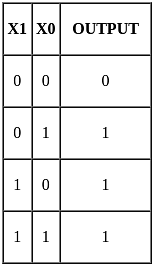
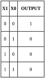
The truth table for ALL options is shown

NAND

From the truth table, it is clear that in NAND gate output is low when all inputs are high

Important Points

OR

AND

NOR

MPPGCL JE Electronics Mock Test - 2 - Question 21
Satellite communication among stations in different areas can be achieved if the satellite has the ability to switch time slots from one beam to another. This is known as satellite switched
Detailed Solution for MPPGCL JE Electronics Mock Test - 2 - Question 21

TDMA:

  • Satellite communication among stations in different areas can be achieved if the satellite has the ability to switch time slots from one beam to another. This is known as time division multiple access (TDMA).
  • In TDMA users transmit in rapid succession, one after the other, each using its time slots.

TSMA:

  • The tone sense multiaccess protocol (TSMA) is designed for packet satellite communications.
  • This protocol is particularly suitable for a satellite system serving an area with a dense population.

FAMA:

  • In fixed- assignment multiple access (FAMA) channels are permanently assigned to terminals.
  • Hence it is also known as a pre-assigned multiple access technique.

SCPC:

  • Single-channel per carrier (SCPC) refers to using a single signal at a given frequency and bandwidth.
  • Most often it is used as on broadcast satellite.
MPPGCL JE Electronics Mock Test - 2 - Question 22

The antenna current of an AM broadcast transmitter, modulated to a depth of 40% by an audio sine wave is 11A. It increases to 12A as a result of simultaneous modulation by another audio sine wave. What is the modulation index due to the second wave?

Detailed Solution for MPPGCL JE Electronics Mock Test - 2 - Question 22

Concept:

Current in single tone modulation:

IT = IC√ ( 1 + μ2/2)

where;

IT → Total current

IC → Carrier's current

μ → Modulation index in single tone modulation

Current in multitone modulation:

 IT = IC√ ( 1 + μt2/2)

where;

 μt = √( μ12 + μ22 + μ32 + ..... ) 

μt → Modulation index due to multitone modulation

Calculation:

Given;

Modulation index at single tone: μ = 40% = 0.4

Total current : IT1 = 11 A

When simultaneous modulation by another audio sine wave.

Total current increased to IT2 = 12 A

Since;

 IT ∝  √ ( 1 + μ2/2)

Hence,

MPPGCL JE Electronics Mock Test - 2 - Question 23
For a BJT, α = 0.97 and collector base junction reverse saturation current is given by 0.4 μA. This BJT is connected in common emitter configuration and operating in active region. If IB = 15 μA then the collector current for the device will be _________
Detailed Solution for MPPGCL JE Electronics Mock Test - 2 - Question 23

Concept: 

ICEO is the reverse leakage current in the common-emitter configuration of BJT when the base is open.

ICBO is the reverse leakage current in the common-base configuration of BJT when the emitter is open.

Also, ICEO > ICBO

And they are related by the relation:

ICEO = (1 + β) ICBO

Total collector current is given by:

IC = βIB + ICBO(β + 1)

Application:

Given that

Common base current gain α = 0.97

So, the common-emitter current gain:

ICO = reverse saturation current = 0.4 μA

IB = Base current = 15 μA

Then collector current is given by  

IC = βIB + (1 + β) ICO

IC = 32.33 × 15 × 10-6 + (1 + 32.33) 0.4 × 10-6 

IC = 498.34 μA

MPPGCL JE Electronics Mock Test - 2 - Question 24

The internet allows to ___.

Detailed Solution for MPPGCL JE Electronics Mock Test - 2 - Question 24

The correct answer is All of the above.

Key Points

  • The Internet is a huge collection of networks, a networking infrastructure. It encapsulates millions of computers together globally, forming a network in which any computer can communicate with any other computer as long as they are both connected to the Internet. In other words, it is a worldwide system of cross-connected computer networks, connecting millions of devices through which exchange of information such as data, news, and opinions, etc. is possible.
  • It utilizes the TCP/IP (Transmission Control Protocol/Internet Protocol) to aid millions of users across the globe. So, TCP/IP can be called the backbone of the Internet. It is considered as a network of networks that consists of thousands of private and public, academic, business, and government interconnections. The Internet is often considered as “The Information Highway”, which implies that there is a straight and clear way of obtaining information. It connects thousands of computer networks. Each device connected to the Internet is known as the host and is independent. Through telephone wires, Fiber optical cable, and satellite links, Internet users can share a variety of information.
  • The Internet is defined as an Information superHighway, to access information over the web. However, It can be defined in many ways as follows:
    • The Internet is a worldwide global system of interconnected computer networks.
    • The Internet uses the standard Internet Protocol (TCP/IP).
    • Each device connected to the internet is identified by its unique IP address.
MPPGCL JE Electronics Mock Test - 2 - Question 25

For the circuit shown, if the resistance of each resistor is 100 ohm, the potential at X is ________.
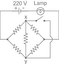
Detailed Solution for MPPGCL JE Electronics Mock Test - 2 - Question 25

The correct answer is option 4):(the same as that of Y)

Concept:

  • The given circuit resembles the wheat stone bridge
  • The Wheatstone bridge works on the principle of null deflection, i.e. the ratio of their resistances is equal, and no current flows through the circuit. Under normal conditions, the bridge is in an unbalanced condition where current flows through the galvanometer. The bridge is said to be balanced when no current flows through the galvanometer.
  • If the resistance of each resistor is 100 ohm, The bridge is at balance condition no current flows in the centre arm. the potential at X is equal to y
MPPGCL JE Electronics Mock Test - 2 - Question 26

A 4 kHz square wave of duty cycle 50% and p-p (0.2V to +0.2V) is applied as input to 20 kHz narrow bandpass filter which is followed by an amplifier of voltage gain 20. Find out the frequency components present in the output. Given that cut off frequencies of a narrow bandpass filter is 20 kHz and 40 kHz.

Detailed Solution for MPPGCL JE Electronics Mock Test - 2 - Question 26

The given

Narrow bandpass filter

T = 0.25 msec

Now applying Fourier series formula on x(t), we get:


ω0T = 2π


So, odd components are a1, a3, a5, a7, a9…., and so on.

Since the filter passes frequencies only between 20 kHz and 40 kHz, the components lying between this band of frequency will be passed by the filter.

The fundamental frequency given is 4 kHz.

a1 = 4 kHz

a3 = 12 kHz


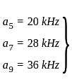
These 3 components of 20 kHz, 28 kHz, and 36 kHz will be passed and the rest of the components will be rejected by the filter.

a11 → 44 kHz

a13 → 52 kHz

       ⋮

And so on

∴ Option 2 is correct.

MPPGCL JE Electronics Mock Test - 2 - Question 27

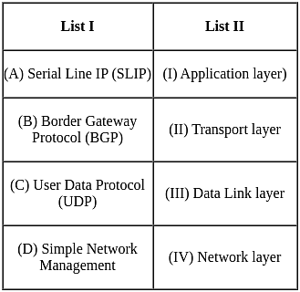
Match List I with List II

Choose the correct answer from the options given below:

Detailed Solution for MPPGCL JE Electronics Mock Test - 2 - Question 27

The correct answer is option 2.

Key Points

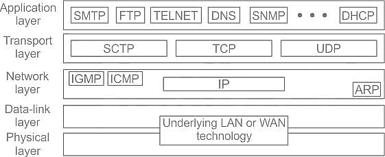
  • Serial Line Internet Protocol (SLIP) is a Data Link layer simple protocol that works with TCP/IP for communication over serial ports and routers. They provide communications between machines that were previously configured for direct communication with each other. 
  • Border Gateway Protocol (BGP) is a Network layer used to exchange routing information for the internet and is the protocol used between ISP which are different ASes.
  • User Datagram Protocol (UDP) is a Transport Layer protocol. UDP is a part of the Internet Protocol suite, referred to as UDP/IP suite. Unlike TCP, it is an unreliable and connectionless protocol.
  • SNMP is an application layer protocol that uses UDP port number 161/162.SNMP is used to monitor the network, detect network faults and sometimes even used to configure remote devices

∴ Hence the correct answer is A-III, B -IV, C -II, D -I.

Additional Information


MPPGCL JE Electronics Mock Test - 2 - Question 28
Bhakra canal has been drawn from which River near Nangal?
Detailed Solution for MPPGCL JE Electronics Mock Test - 2 - Question 28

The correct answer is Satluj.

  • Bhakra canal has been drawn from the Satluj River near Nangal.

Key Points

  • It’s a concrete gravity dam located in Bilaspur, Himachal Pradesh.
  • Govind Sagar reservoir is formed by the dam.
  • The length of the dam is 518.25 m and the width of the dam is 9.1 m.
  • The reservoir of the dam is known as Govind Sagar.
  • Bhakra dam has created a 90 km long reservoir.
  • Pandit Jawaharlal Nehru described the dam as the “New temple of resurgent India”.
MPPGCL JE Electronics Mock Test - 2 - Question 29

The name of the famous mathematician who is credited with discovering the total value of the very first 100 natural numbers is

Detailed Solution for MPPGCL JE Electronics Mock Test - 2 - Question 29

Gauss is the great mathematician who is credited with discovering the total value of the first 100 natural numbers.

MPPGCL JE Electronics Mock Test - 2 - Question 30

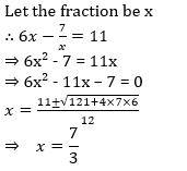
6 times of a fraction is greater than 7 times of its reciprocal by 11. What is the fraction? 

Detailed Solution for MPPGCL JE Electronics Mock Test - 2 - Question 30

View more questions
Information about MPPGCL JE Electronics Mock Test - 2 Page
In this test you can find the Exam questions for MPPGCL JE Electronics Mock Test - 2 solved & explained in the simplest way possible. Besides giving Questions and answers for MPPGCL JE Electronics Mock Test - 2, EduRev gives you an ample number of Online tests for practice

Top Courses for Electronics and Communication Engineering (ECE)

Download as PDF

Top Courses for Electronics and Communication Engineering (ECE)