MPPGCL JE Electronics Mock Test - 5 - Electronics and Communication Engineering (ECE) MCQ
30 Questions MCQ Test - MPPGCL JE Electronics Mock Test - 5

Calculate the baud rate of the ASK signal having a bit rate of 300 bps.
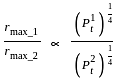
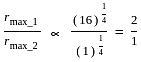
Two radars are transmitting powers P1 and P2. If the transmitted power P1 is 16 times the transmitted power P2 and all other parameters are same then ratio of maximum range of radar 1 to radar 2 is:


| 1 Crore+ students have signed up on EduRev. Have you? Download the App |
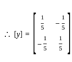
The y-parameters for the network shown in the figure can be represented by


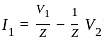 ...1)
...1)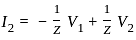 ...2)
...2)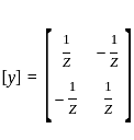
In VCO IC 566, the value of charging & discharging is dependent on the voltage applied at ________.

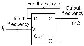
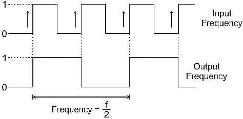
If the input to T-flipflop is 200 Hz signal, the final output of the three T- flipflops in cascade is

For an AM signal, the bandwidth is 6 kHz and the highest frequency component present is 600 kHz. The carrier frequency used for this AM signal is

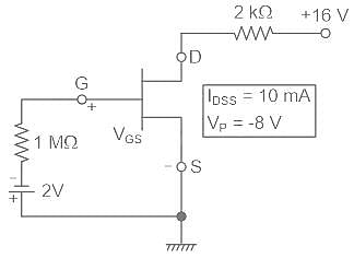
Determine the VDS of FET network given below -

By narrowing the space charge region, the amount of reverse voltage needed to cause zener breakdown:

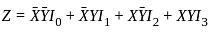
The logic function implemented by the following 4: 1 MUX is:


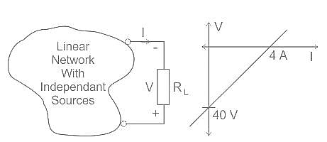
RL given in the below figure is variable resistance, find the maximum power transferred to that resistance. V vs I characteristic is also sown below.

 Vth = - 40 V
 Vth = - (-40 V) = 40 V


Which of the following is NOT the advantage of half-wave rectifier?

In a radar system, if the peak transmitted power is increased by a factor of 16 and the antenna diameter is increased by a factor of 2, then the maximum range will increase by a factor of


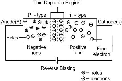
Which of the following diode is used as detector in radar?

A silicon sample A is doped with 1018 atom/cm3 of Boron and another silicon sample B of identical dimensions is doped with 1018 atom/cm3 of Phosphorous. If the ratio of electron to hole mobility is 3, then the ratio of conductivity of sample A to that B is:
 ---(1)
 (For semiconductors doped with donor impurities only)
 (For semiconductors doped with acceptor impurities only)


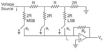
A 4-bit R-2R digital to analog converter (DAC) has a reference of 5 Volts. What is the analog output for input code 1010?

 ⋯ (ii)


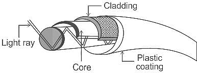
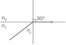
The critical angle θc in an optical fiber is given by ______. Where n1 is refractive index of medium 1 and n2 is the refractive index of medium 2.

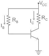
For the base bias circuit, RB = 470 kΩ, RC = 2.2kΩ, and VCC = 18V and the transistor has an hFE of 100. Find VCE.


What are the fields that packet filter network firewall can investigate and block the user using it?
I. Port number of users
II. IP address of users
III. MAC address of users

Determine the type of filter for the following difference equation:
y[n] = x[n] - x[n-1]

Consider the following statements regarding differential pulse-code modulators:
1. The differential pulse-code modulator system employs a predictor.
2. It needs far fewer bits per each error sample than what would have been needed for the original samples themselves.
3. It will have larger dynamic range than the original message itself.
Select the correct statements using the code given below,

What is to be added to 40% of 900 so that the sum must be equal to 30% of 2600?
What is the government formed by an alliance of two or more political parties called?
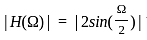
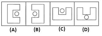
Which figure from the answer figures will replace the question mark (?) in the problem figures?
Problem Figures:

Answer Figures:
Directions: Each of the following consists of a question and two statements numbered I and II given below it. You have to decide whether the data provided in the statements are sufficient to answer the question.
What is Rahul's rank in the class?
Statement I: Rahul's rank is 28 less than Monika's rank.
Statement II: Aditi's rank is 42 more than Rahul's rank. Monika's rank is 12 less than Aditi's rank.
Top Courses for Electronics and Communication Engineering (ECE)


Important Questions for MPPGCL JE Electronics Mock Test - 5
MPPGCL JE Electronics Mock Test - 5 MCQs with Answers
Online Tests for MPPGCL JE Electronics Mock Test - 5
|
© EduRev
|
Education Revolution
|


|


