Electronics and Communication Engineering (ECE) Exam  >  Electronics and Communication Engineering (ECE) Tests  >  MPPGCL JE Electronics Mock Test - 9 - Electronics and Communication Engineering (ECE) MCQ

MPPGCL JE Electronics Mock Test - 9 - Electronics and Communication Engineering (ECE) MCQ


Test Description

30 Questions MCQ Test - MPPGCL JE Electronics Mock Test - 9

MPPGCL JE Electronics Mock Test - 9 for Electronics and Communication Engineering (ECE) 2025 is part of Electronics and Communication Engineering (ECE) preparation. The MPPGCL JE Electronics Mock Test - 9 questions and answers have been prepared according to the Electronics and Communication Engineering (ECE) exam syllabus.The MPPGCL JE Electronics Mock Test - 9 MCQs are made for Electronics and Communication Engineering (ECE) 2025 Exam. Find important definitions, questions, notes, meanings, examples, exercises, MCQs and online tests for MPPGCL JE Electronics Mock Test - 9 below.
Solutions of MPPGCL JE Electronics Mock Test - 9 questions in English are available as part of our course for Electronics and Communication Engineering (ECE) & MPPGCL JE Electronics Mock Test - 9 solutions in Hindi for Electronics and Communication Engineering (ECE) course. Download more important topics, notes, lectures and mock test series for Electronics and Communication Engineering (ECE) Exam by signing up for free. Attempt MPPGCL JE Electronics Mock Test - 9 | 100 questions in 120 minutes | Mock test for Electronics and Communication Engineering (ECE) preparation | Free important questions MCQ to study for Electronics and Communication Engineering (ECE) Exam | Download free PDF with solutions
MPPGCL JE Electronics Mock Test - 9 - Question 1

The electrical resistivity of the material of a conductor is ρ. If its length is doubled and area of cross-section is tripled, then its electrical resistivity will be

Detailed Solution for MPPGCL JE Electronics Mock Test - 9 - Question 1

CONCEPT:

  • Resistivity (ρ): The property of a conductor that opposes the flow of electric current through them and is independent of the shape and size of the materials but depends on the nature and temperature of the materials is called resistivity.
    • The unit for resistivity is the ohm-meter (Ω-m).
    • The resistivity of a material depends on its nature and the temperature of the conductor.
    • The resistivity of a material doesn't depend on its shape and size (length and area).
  • Resistance: The property of any conductor that opposes the flow of electric current through it and depends on the shape and size of the materials, temperature, and nature of the materials is called resistance.
    • It is denoted by R and the SI unit is the ohm (Ω).
  • The resistance is given by:

R = ρL/A

where ρ is resistivity, L is the length and A is the area of the cross-section. 

EXPLANATION:

  • From the above discussion, we can say that when the length is doubled and the area of cross-section is tripled-
  • The resistivity of the material will not change (remain the same, ρ) as it is independent of the length or cross-section of the wire. So option 1 is correct.

EXTRA POINTS:

Difference between resistivity and resistance:

MPPGCL JE Electronics Mock Test - 9 - Question 2

How many number of 2-input NAND gates are required to realise a half adder circuit?

Detailed Solution for MPPGCL JE Electronics Mock Test - 9 - Question 2

Half Adder using NAND Gates:

The half adder can also be designed with the help of NAND gates. NAND gate is considered as a universal gate. A universal gate can be used for designing any digital circuitry. It is always simple and efficient to use the minimum number of gates in the designing process of our circuit. The minimum number of NAND gates required to design a half adder is 5.

  • The first NAND gate takes the inputs which are the two 1-bit numbers.
  • The resultant NAND-operated inputs will be again given as input to 3- NAND gates along with the original input. 
  • Out of these 3 NAND gates, 2-NAND gates will generate the output which will be given as input to the NAND gate connected at the end.
  • The gate connected at the end will generate the sum bit. Out of the 3 considered NAND gates, the third NAND gate will generate the carry bit.
MPPGCL JE Electronics Mock Test - 9 - Question 3

In a 8-bit ripple carry adder using identical full adders, each full adder takes 34 ns for computing sum. If the time taken for 8-bit addition is 90 ns, find time taken by each full adder to find carry

Detailed Solution for MPPGCL JE Electronics Mock Test - 9 - Question 3

Formula:

The total time taken by the for ‘n’ bit ripple carry adder is

Td = (n – 1) tc + Maximum(tc, ts)

tc = delay for carry through a single flip flop.

ts = delay for sum

Data:

Each full adder takes 34 ns for computing

From this, Maximum(tc, ts) = ts = 34 ns

Td = 90 ns.

n = 8

Calculation:

Td = (n – 1) tc + Maximum(tc, ts)

90 = (8 – 1)tc + 34

7tc = 56 ns.

tc = 8 ns.

Time taken by each full adder to find carry is 8 ns.

Hence, the correct answer is option 4.

MPPGCL JE Electronics Mock Test - 9 - Question 4

For the signal flow graph shown in the figure, determine the overall transmittance relating C and R.

Detailed Solution for MPPGCL JE Electronics Mock Test - 9 - Question 4

Solution 

In the above SFG, G2 and G1 are in parallel,

they can be represented as G2+G1

Hence we get the overall SFG equivalent as shown below

The above represents a general block diagram simplified to maximum extent 

Also, the closed-loop transfer function is given by =

  • where GH is the open-loop transfer function
  •  G is the forward block transfer function

Comparing it with our equivalent SFG, we have G= (G2+G1)

H=H1, so GH=(G2+G1)H1

Hence we have an overall transmittance, =

Therefore the correct option is 3.

MPPGCL JE Electronics Mock Test - 9 - Question 5

A semiconductor bar having a length of 4 cm is subjected to a voltage of 8 Volts. If the average drift velocity is 104 cm/s, then electron mobility would be:

Detailed Solution for MPPGCL JE Electronics Mock Test - 9 - Question 5

Concept:

Mobility of charge carriers (μ) defines how fast the charge carriers or travel from one place to another.

It is drift velocity (saturation velocity) per unit electric field. i.e

 -----(1)

vd = Drift velocity (Saturation velocity)

E = Electric field given by:

 -----(2)

Calculation:

L = 4 cm

V = 8 Volts

vd = 104 cm/s

from Equation (2):

From equation (1):

Important Point

  • Mobility increases due to lattice scattering and decreases due to impurity scattering
  • At low temperatures only impurity scattering is dominant and at high temperatures lattice scattering is dominant
  • Mobility first increases with temperature and then subsequently decreases

Note: The term impurity in an intrinsic semiconductor:

Impurity scattering is caused by crystal defects such as ionized impurities.

At lower temperatures, carriers move more slowly, so there is more time for them to interact with charged impurities.

As a result, as the temperature decreases, impurity scattering increases, and mobility decreases.

The effect is just the opposite of the effect of lattice scattering.

MPPGCL JE Electronics Mock Test - 9 - Question 6
In data communication, jitter refers to ___________
Detailed Solution for MPPGCL JE Electronics Mock Test - 9 - Question 6

The effective of a data communications system depends on four fundamental characteristics:

Delivery, Accuracy, Timeliness and Jitter.

Delivery: The system must deliver data to the correct destination; Data must be received by the intended device or user

Accuracy: The system must deliver the data accurately; Data that have been altered in transmission and left uncorrected are unusable

Timeliness: The system must deliver data in a timely manner; Data delivered late are useless

Jitter: Jitter refers to the variation in the packet arrival time; It is the uneven delay in the delivery of audio or video packets
MPPGCL JE Electronics Mock Test - 9 - Question 7
The orbital period of communication satellites is _______ as that of earth’s rotational period.
Detailed Solution for MPPGCL JE Electronics Mock Test - 9 - Question 7
The communication satellite is in circular orbit and has orbital period same as that of the earth’s rotational period.
MPPGCL JE Electronics Mock Test - 9 - Question 8

For the logic circuit shown in the following figure, representation of the state diagram is:

Detailed Solution for MPPGCL JE Electronics Mock Test - 9 - Question 8

Concept:

For D flip-flop, the next state output (Qn+1) from the present state input (Qn) is given by:

Qn+1 = D

Explanation:

MPPGCL JE Electronics Mock Test - 9 - Question 9

The above circuit can be represented in the frequency domain as:

Detailed Solution for MPPGCL JE Electronics Mock Test - 9 - Question 9

Concept:

Inductive impedance is given by:

jXL = jωL

ω = frequency in radian/sec which can be written as:

ω = 2πf

f  = frequency in Hz

L = value of inductor in Henry

Similarly, the capacitive impedance is given by:

Calculation:

Given ω = 50 rad/sec

The capacitive reactance of the capacitor with C = 1000 μF will be:

The capacitance will, therefore be replaced with  -20j

Similarly, the inductor will be replaced with:

jωL = j × 50 × 500 mH

jωL = 25j

The resultant circuit will be, therefore:

MPPGCL JE Electronics Mock Test - 9 - Question 10

Find the volume charge density that is associated with the field D = ar C/m2

Detailed Solution for MPPGCL JE Electronics Mock Test - 9 - Question 10

Concept:

Volume charge density is given by the formula Pv

Calculation:

For spherical coordinates  =  having only  component

∴ 

MPPGCL JE Electronics Mock Test - 9 - Question 11

Match the following:

Detailed Solution for MPPGCL JE Electronics Mock Test - 9 - Question 11

The correct option is (3)

1 → IV, 2 → II, 3 → I, 4 → V, 5 → III

Key Points

  • Bus topology → Each communicating device connects to a transmission medium.
  • Ring topology → Each node is connected to two other devices, one each on either side.
  • Mesh topology → Each communicating device is connected with every other device.
  • Star topology → Each communicating device is connected to a central node.
  • Hybrid topology → Each branch can have one or more basic topologies.​

Additional Information 

  • BUS topology:- In a bus topology, each communicating device connects to a transmission medium, known as a bus. Data sent from a node are passed on to the bus and hence are transmitted to the length of the bus in both directions. 
  • Ring topology:- In a ring topology, each node is connected to two other devices, one each on either side. The nodes connected with each other thus form a ring. 
  • Mesh topology:- In this topology, each communicating device is connected with every other device in the network. Such a network can handle large amounts of traffic since multiple nodes can transmit data simultaneously. 
  • Star topology:- In star topology, each communicating device is connected to a central node, which is a networking device like a hub or switch.
  •  Hybrid topology:- It is a hierarchical topology, in which there are multiple branches and each branch can have one or more basic topologies like a star, ring, and bus. 
MPPGCL JE Electronics Mock Test - 9 - Question 12

When the area of the parallel plate capacitor increases by 7 times and separation between both plates decreases by 7 times, then the capacitance of the parallel plate capacitor becomes

Detailed Solution for MPPGCL JE Electronics Mock Test - 9 - Question 12

Concept:

The capacitance of a capacitor (C): The capacitance of a conductor is the ratio of charge (Q) to it by a rise in its potential (V), i.e.

C = Q/V

For a Parallel Plate Capacitor:

parallel plate capacitor consists of two large plane parallel conducting plates of area A and separated by a small distance d.

Mathematical expression for the capacitance of the parallel plate capacitor is given by:

Where C = capacitance, A = area of the two plates, ε = dielectric constant (simplified!), d = separation between the plates.

The unit of capacitance is the farad, (symbol F ).

Calculation:

According to the question area of the parallel plate capacitor increases by 7 times and separation between both plates decreases by 7 times

∴ A' = 7 A

∴ 

C' = 49 C

MPPGCL JE Electronics Mock Test - 9 - Question 13

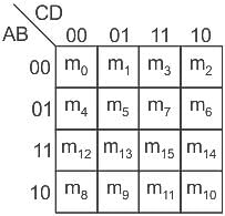
There are 4 variables in the Boolean function and the value of the function is 1. Find the number of cells in the K-Map which will contain a 1 when SOP expression is used.

Detailed Solution for MPPGCL JE Electronics Mock Test - 9 - Question 13

Concept:

The K-map is a graphical method that provides a systematic method for simplifying and manipulating the Boolean expressions or to convert a truth table to its corresponding logic circuit in a simple, orderly process.

In an 'n' variable K map, there are 2n cells.

Application:

For 4 variables there will be 24 = 16 cells

The K map will give an output of 1, when all the cells have a 1, i.e. if all the input combinations give an output of 1, the maximum number of inputs can be simplified to give an output of 1.

This is explained with the following K map:

Since the K map forms a pair of 16, it can be eliminated giving an output:

Y = 1

Since the output contains no input variables (A, B, C, or D), all the four variables are simplified/eliminated.

MPPGCL JE Electronics Mock Test - 9 - Question 14

For which of the following ROCs, Fourier transforms is not defined?

Detailed Solution for MPPGCL JE Electronics Mock Test - 9 - Question 14
  • The Fourier transform of a function is equal to its two-sided Laplace transform evaluated on the imaginary axis of the s-plane.
  • The main drawback of Fourier transform (i.e. continuous F.T.) is that it can be defined only for stable systems, Whereas, Laplace Transform can be defined for both stable and unstable systems.
  • An LTI system is stable if and only if the ROC of its system function H(s) includes the jω-axis [i.e., Re{s} = 0]  
  • Fourier transform is defined only for stable signals. 
  • From the given ROCs, B and C does not include the jω axis thus Fourier transform is not defined for B & C.
MPPGCL JE Electronics Mock Test - 9 - Question 15

Which are the three basic types of motion control systems in numerical control?

Detailed Solution for MPPGCL JE Electronics Mock Test - 9 - Question 15
  • The three basic types of the motion control systems in numerical control are:

​1. Point to Point (PTP) Control System

2. Straight-line Control System

3. Contour Control System

Point to Point (PTP) Control System:

  • When only the endpoint movement of a tool is important whereas the path followed by the tool in between endpoint movement is not important is called point to point control system.

  • In the PTP control system, only one axis movement of a tool is sufficient.

          For Ex. Drilling, Reaming, Tapping, Boring Spot welding, punching, blanking, etc.

Straight-line Control System:

  • In addition to the endpoint movement of a tool in the path followed by the tool is also important and if it is a straight-line path it is called a straight line Control system.
  • Here 2- axes simultaneously movement is required.

  • Ex. Straight turning, taper turning, shaping, planning, creating a straight Milling slot, etc.

​Contour Control System:

  • In addition to the endpoint movement of the tool if a path followed by the tool is also important and if it is a contour path, it is called a contour control system.

          Here, 3 – axes simultaneous movement of the tool is required.


  • But it is highly impossible to manufacture a perfect contour in the reality, whereas a contour is constructed by much linear distance travel of a tool between two consecutive points i.e. by Interpolation.
MPPGCL JE Electronics Mock Test - 9 - Question 16

Which bus is used to specify memory locations for the data being transferred

Detailed Solution for MPPGCL JE Electronics Mock Test - 9 - Question 16

Concept:

The following figure shows the connection of buses between the microprocessor and memory

From the figure:

Address Bus:

An address bus is a bus that is used to specify a physical address. When a processor or DMA-enabled device needs to read or write to a memory location, it specifies that memory location on the address bus (the value to be read or written is sent on the data bus)

Data Bus:

It is a bi-directional bus.

Data and Instructions pass through this bus to reach the microprocessor.

This is responsible for the exchange of information between the main memory and microprocessor.

Control Bus:

This is a unidirectional bus.

This tells whether read or write, which operation should be performed that is in which direction the data should flow.

MPPGCL JE Electronics Mock Test - 9 - Question 17
For open loop transfer function of a unit feedback is G(s) = , having peak overshoot 10%. Find damping ratio.
Detailed Solution for MPPGCL JE Electronics Mock Test - 9 - Question 17

Solution

Concept

For a 2nd order underdamped system, the maximum  percentage overshoot is given by

Mp%=  × 100 %

here ζ is the damping ratio

Calculation 

Given, Mp% =10%

 =  

0.1=

ln(0.1)= 

-2.302= 

0.733=

Squaring and cross multipicating we get

1=2.8596 ζ2

ζ =0.59 ≈0.60

Hence the damping ratio is 0.6

Therefore the correct option is 2

MPPGCL JE Electronics Mock Test - 9 - Question 18

Output data ratio of a 8-bit PCM-TDM system sampling 24 voice channels, comparing these using μ-law at the rate of 8 kHz with a 1 frame alignment word, is:

Detailed Solution for MPPGCL JE Electronics Mock Test - 9 - Question 18

Pulse-code modulation(PCM):

  • Pulse-code modulation (PCM) is a process used to digitally represent sampled analog or continuous-time signals.
  • It is the reference form of digital in computers, CDs, digital telephony, and other digital audio applications. 
  • The amplitude of the continuous-time signal is sampled at uniform intervals and each sample is quantized to its nearest value within a predetermined range of digital levels.

Time-division multiplexing(TDM):

Time-division multiplexing (TDM) is a process of transmitting and receiving independent signals over a common signal path by means of synchronized switches at each end of the transmission line so that each signal appears on the line only a fraction of time in an alternating pattern.

PCM-TDM system:

  • PCM with time-division multiplexing, transmissions from multiple sources occur in the same facility but not at the same time.
  • The multiplexer is simply an electrically controlled digital switch with two inputs and one output.
  • One 8-bit PCM code from each channel (16-bits total) is called a TDM frame, and the time it takes to transmit one TDM frame is called frame time.
  • The frame time is reciprocal of the sample rate.
  • The PCM code for each channel occupies a fixed time slot within the total TDM frame.
  • Output data ratio(Rb) = 1 / Tb . Where Tb is time for each bit.

Calculation:

Given that 

Each frame consists of 24 8-bit words, plus a single synchronizing bit.

Total number of pulses sent over sampling period = 24 × 8 + 1 = 193

Sampling frequency (fs) = 8 kHz

Sampling Time(Ts) = 1 / fs = 1 / 8 kHz = 0.125 ms

Time for each bit(Tb) = Ts / 193 = 0.648 μs

Output data ratio(Rb) = 1 / Tb = 1 / 0.648 μs = 1.544 mbps ≈ 1.6 × 106 bits/sec.

Alternative method:

Rb = sampling frequency × total number of pulses over Ts 

= 8 × 103 × 193 

= 1.544 mbps ≈ 1.6 × 106 bits/sec

MPPGCL JE Electronics Mock Test - 9 - Question 19

Match List-I with List-II and select the correct answer using the code given below the lists-

Detailed Solution for MPPGCL JE Electronics Mock Test - 9 - Question 19

The correct match is 

A - (1), B - (4), C - (3), D - (2)

(A) Huffman code → (1) Elimination of redundancies

(B) Error-correcting → (4) channel coding

(C) NRZ-coding → (3) Adapts the transmitted signal to the line

(D) Delta modulation → (2) Reduces bit rate

(A)- Huffman code

  • It is a popular technique to remove coding redundancy
  • The result after Huffman are of variable length
  • The codewords are of unequal lengths

(B)- Error-correcting codes

  • Error-correcting codes(ECC) are used for controlling errors in data over noisy communication channels 
  • The sender encodes the message with redundant information in form of ECC 
  • This redundancy allows the receiver to detect the minimum number of errors and correct it

(C)- NRZ coding 

  • it is used in slow-speed synchronous and asynchronous transmission interfaces
  • Logic1 is sent as a high voltage value
  • Logic 0 is sent as a low voltage value

(D)- Delta modulation

  • Analog to digital conversion technique used to transmit voice signals 
  • It is the simplest form of DPCM(differential pulse code modulation) 
  • Here transmission of data is reduced to 1 bit data stream

Hence the correct option is 3

MPPGCL JE Electronics Mock Test - 9 - Question 20
A continuous-time signal x(t) = 2 cos (100 πt) is sampled at a sampling rate of 75 Hz to generate a sequence x(n). The frequency of a sinusoid that yields samples identical to x(n).
Detailed Solution for MPPGCL JE Electronics Mock Test - 9 - Question 20

Given x(t) = 2 cos (100 πt)

Sampling Frequency = 75 Hz

Time period (T) after which the samples are being taken is:

Replacing t with nTs, we get the discrete-time sequence as:

x(n) = x(nTs)

The fundamental period of the above sequence will be:

N = minimum value for which the above becomes an integer.

So, the sequence x(n) is periodic with a fundamental period of 3 sec.

The frequency of a sinusoid that will yield the same samples identical to x(n) will be:

MPPGCL JE Electronics Mock Test - 9 - Question 21
In a fullwave rectifier circuit with centre tap transformer, if voltage between one end of secondary winding and centre tap is 300 V peak, then PIV (peak inverse voltage) is
Detailed Solution for MPPGCL JE Electronics Mock Test - 9 - Question 21

Concept:

Peak Inverse Voltage:

1. It is the max voltage that appears across the diode when it is in non conducting state or in reverse biased in a rectifier.

2. For safe operation of the diode, peak inverse voltage should be less than the breakdown voltage.

PIV = |Vdiode|max

PIV = Vm  in case of a half-wave rectifier.

In center-tapped full-wave rectifier,

1. The secondary winding is center tapped i.e. secondary winding is divided into two halves.

2. In case of a center-tapped full-wave rectifier:

PIV = 2V----(1)

3. Greater PIV is a disadvantage because devices with greater breakdown voltage will be needed which are costlier.

Calculation:

Given:

Vm = 300 V

From equation (1)

PIV = 2 × 300

PIV = 600 V

Hence option (3) is the correct answer.

MPPGCL JE Electronics Mock Test - 9 - Question 22

Consider a cascade system with unit step u(t) as input and h1(t) = e-2t u(t)  and h2(t) = e-t u(t) respectively. The impulse response of overall system is:

Detailed Solution for MPPGCL JE Electronics Mock Test - 9 - Question 22

Concept:

Some important convolution results are

  • u(t) * u(t) = t u(t)
  • e­-at u(t) * e­-at u(t) = t e­-at u(t)
  • e­-t u(t) * u(t) = (1- e­-t) u(t)
  •   

Calculation:

h1(t) = e-2tu(t)  and h2(t) = e-tu(t)

Now convolution

h(t) =  h1(t) * h2(t)

h(t) =  [e-t – e-2t]u(t)

MPPGCL JE Electronics Mock Test - 9 - Question 23

Direction: In the following question, the sentences have been given in Active/ Passive Voice. From the given alternatives, choose the one that best expresses the given sentence in Passive/ Active Voice.

She took the dog for a walk.

Detailed Solution for MPPGCL JE Electronics Mock Test - 9 - Question 23

The sentence is in active voice and to convert it in passive voice the predicate of the sentence becomes the subject.
Use structure “auxiliary + past participle”
As per the given above sentence is given in Passive Voice.
The dog was taken for a walk by her.
Hence , required answer will be option C .

MPPGCL JE Electronics Mock Test - 9 - Question 24

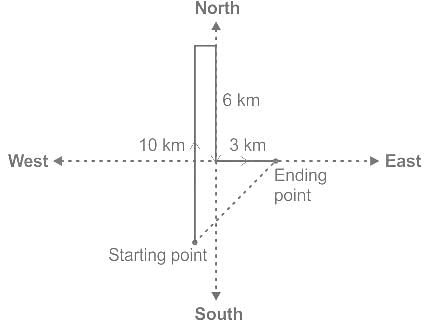
Mr. X walks 10 km towards the North. From there it is 6 km towards south then moves 3 km to the east. In which direction is he now standing from his starting point?

Detailed Solution for MPPGCL JE Electronics Mock Test - 9 - Question 24

i) Mr. X walks 10 km towards the North.

ii) From there it is 6 km towards the south then moves 3 km to the east.

According to the information given in the question, we can draw the following diagram.

Thus we can see he is standing in a North-East direction from his starting point.

Hence, the correct answer is "North-East".

MPPGCL JE Electronics Mock Test - 9 - Question 25

How many triangle in figure?

Detailed Solution for MPPGCL JE Electronics Mock Test - 9 - Question 25

In the given figure, we can identify multiple triangles. By counting the individual triangles, we can determine that there are a total of 12 triangles in the figure.

MPPGCL JE Electronics Mock Test - 9 - Question 26

Directions to Solve

Each of the following questions has a group. Find out which one of the given alternatives will be another member of the group or of that class.

Question -

Pathology, Cardiology, Radiology, Ophthalmology

Detailed Solution for MPPGCL JE Electronics Mock Test - 9 - Question 26

As all terms given in the question are medical terms and Hematology is also medical term.

MPPGCL JE Electronics Mock Test - 9 - Question 27

When did Jawaharlal Nehru give his famous speech ‘Tryst with Destiny’?

Detailed Solution for MPPGCL JE Electronics Mock Test - 9 - Question 27
Answer:
Background:
Jawaharlal Nehru was the first Prime Minister of India and played a crucial role in the Indian independence movement. He gave his famous speech, "Tryst with Destiny," on the eve of India's independence.

Jawaharlal Nehru gave his famous speech, "Tryst with Destiny," on 15th August 1947, at midnight.
Explanation:
The correct answer is option C - 15 August 1947 midnight. Here's a detailed explanation:
- Jawaharlal Nehru gave his famous speech, "Tryst with Destiny," on the night of India's independence.
- The speech was delivered on 15th August 1947, when India gained independence from British rule.
- The speech marked the beginning of a new era for India and outlined the vision for the nation's future.
- Nehru emphasized the ideals of freedom, democracy, and equality for all citizens of India.
- The speech is considered one of the most significant speeches in Indian history and is often referred to as the "Tryst with Destiny" speech.
- Nehru's speech highlighted the challenges and opportunities that lay ahead for India as a newly independent nation.
Therefore, the correct answer is option C - 15 August 1947 midnight.
MPPGCL JE Electronics Mock Test - 9 - Question 28

The Indian Constitution prescribes Fundamental Rights in :

Detailed Solution for MPPGCL JE Electronics Mock Test - 9 - Question 28

The correct option is A.
The Fundamental Rights are defined as the basic human rights of all citizens. These rights, defined in Part III of the Constitution, applied irrespective of race, place of birth, religion, caste, creed, or gender. They are enforceable by the courts, subject to specific restrictions.

MPPGCL JE Electronics Mock Test - 9 - Question 29

Which of the following freedoms is not available to an Indian citizen?

Detailed Solution for MPPGCL JE Electronics Mock Test - 9 - Question 29

Freedom available to Indian citizens:
- Freedom to criticise the government
- Freedom to reside in any part of the country
Freedom not available to Indian citizens:
- Freedom to participate in armed rebellion
Explanation:
- Indian citizens have the freedom to criticise the government. This means they have the right to express their opinions, voice their concerns, and hold the government accountable for its actions and policies.
- Indian citizens also have the freedom to reside in any part of the country. They can choose to live and work in any state or union territory without any restrictions.
- However, the freedom to participate in armed rebellion is not available to Indian citizens. Engaging in armed rebellion or taking up arms against the government is considered a criminal act and is punishable under the law.
Conclusion:
In summary, Indian citizens have the freedom to criticise the government and the freedom to reside in any part of the country. However, they do not have the freedom to participate in armed rebellion.
MPPGCL JE Electronics Mock Test - 9 - Question 30

The distance from the equator to either of the poles is one-fourth of a circle round the earth and it will measure ¼ of ………….. degree.

Detailed Solution for MPPGCL JE Electronics Mock Test - 9 - Question 30

A full circle is 360 degrees. The distance from the equator to either of the poles is one-fourth of the circumference of the Earth. Since a circle measures 360 degrees, one-fourth of that circle (representing the distance from the equator to either pole) would also measure ¼ of 360 degrees, which is 90 degrees.

View more questions
Information about MPPGCL JE Electronics Mock Test - 9 Page
In this test you can find the Exam questions for MPPGCL JE Electronics Mock Test - 9 solved & explained in the simplest way possible. Besides giving Questions and answers for MPPGCL JE Electronics Mock Test - 9, EduRev gives you an ample number of Online tests for practice
Download as PDF