MPPGCL JE Electronics Mock Test - 10 - Electronics and Communication Engineering (ECE) MCQ
30 Questions MCQ Test - MPPGCL JE Electronics Mock Test - 10


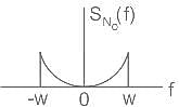
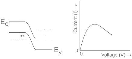
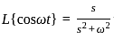
 (for envelope detector).
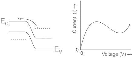

Which information is displayed in the fire control room?
| 1 Crore+ students have signed up on EduRev. Have you? Download the App |
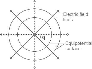
For an isotropic radiator, electric field intensity at a distance R is measured as 3 V/m. What will be the electric field intensity at a distance 3 R?


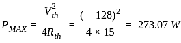
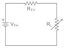
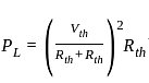
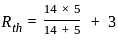
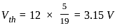
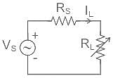
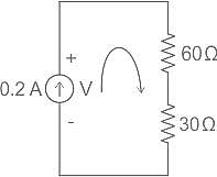
What is maximum power delivered to the load ?
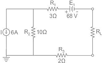

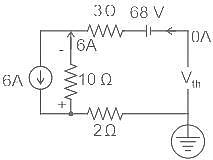
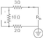
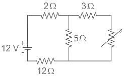
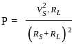
What will be the maximum power that can be distributed in the load in the given circuit?


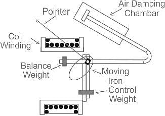
Moving iron instruments are scaled at ______.
A voltmeter has resistance of 2000 Ω, when it is connected across a DC circuit its power consumption is 2 mW. Suppose this voltmeter is replaced by a voltmeter of 4000 Ω resistance, the power consumption will be:
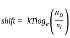
 increases and the shift increases.
How many roots of characteristic equation P(s) = s4 + s3 + 2s2 + 2s + 3 have (+)ve real part?

 we get negative infinite, which means we get two significant changes on the first column means two poles at the right-hand side of the origin.
Consider the purely resistive circuit as shown in Fig. where, VS is the source voltage, RS is the source resistance, RL is the load resistance and IL is the load current. The current at maximum power is equal to _______ of the maximum current.


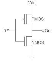
Which of the following parameters are affected due to short-channel MOSFET geometry
I. Mobility of carriers
II. Threshold voltage
III. Drain current

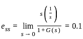
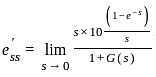
The steady-state error for a system is 0.1. Steady-state error for the previously mentioned system being closed loop with a unity negative feedback and pulse input for 1 sec having a magnitude of 10 is?


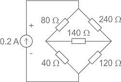
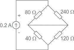
A Wheatstone bridge with resistors as shown in figure is connected to a 0.2 A current source. Find the voltage across the 0.2 A current source, if the 140 Ω resistor is shorted.


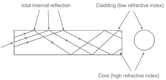
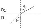
Which of the following is the principle of operation of fibre-optic cable?
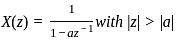
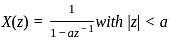
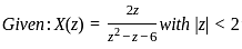
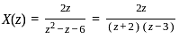
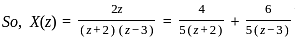
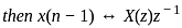
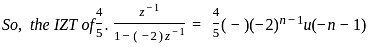
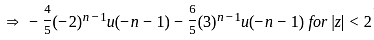
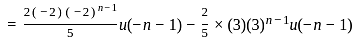
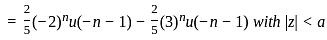
What is the inverse z-transform of  with ROC |z| < 2


 ?
?


Direction: If a Paper (Transparent Sheet) is folded in a manner and a design or pattern is drawn. When unfolded this paper appears as given below in the answer figure. Choose the correct answer figure given below.
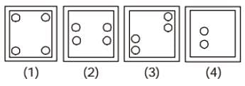
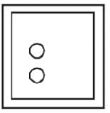
If a paper is folded in a particular manner and punch is made, when, unfolded this paper appears as given below in the question figure. Find out the manner in which the paper is folded and the punch is made from the answer figures given.
Question Figure
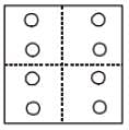
Answer figure
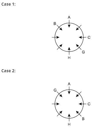
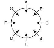
Direction: Study the following information carefully and answer the given questions besides.
Eight person A, B, C, D, E, F, G and H sit around the circular table facing towards the centre but not necessarily in the same order.
G sits opposite to B. One person sits between A and C, who sits second to the right of H. Both G and B do not sit immediate left of H. D sits second to the left of B. A doesn’t sit beside D. E doesn’t face C.
Q. Who sits opposite to F?
Directions: In each of the following questions, a sentence has been given in Active (or Passive) Voice. Out of the four alternatives suggested, select the one that best expresses the same sentence in Passive/ Active Voice.
They will have completed the work by the time we get there.
Directions to Solve
In each of the following questions find out the alternative which will replace the question mark.
Question -
27 : 125 :: 64 : ?
Direction: A word in capital letters is followed by four words. Choose the word that is most nearly opposite in meaning to the word given in capital letters.
MANSION
Direction: A word in capital letters is followed by four words. Choose the word that is most nearly opposite in meaning to the word given in capital letters.
TRACTABLE
Top Courses for Electronics and Communication Engineering (ECE)


Important Questions for MPPGCL JE Electronics Mock Test - 10
MPPGCL JE Electronics Mock Test - 10 MCQs with Answers
Online Tests for MPPGCL JE Electronics Mock Test - 10
|
© EduRev
|
Education Revolution
|


|


