Electrical Engineering (EE) Exam  >  Electrical Engineering (EE) Tests  >  Test: Electronic Devices & Circuits - 3 - Electrical Engineering (EE) MCQ

Test: Electronic Devices & Circuits - 3 - Electrical Engineering (EE) MCQ


Test Description

25 Questions MCQ Test - Test: Electronic Devices & Circuits - 3

Test: Electronic Devices & Circuits - 3 for Electrical Engineering (EE) 2024 is part of Electrical Engineering (EE) preparation. The Test: Electronic Devices & Circuits - 3 questions and answers have been prepared according to the Electrical Engineering (EE) exam syllabus.The Test: Electronic Devices & Circuits - 3 MCQs are made for Electrical Engineering (EE) 2024 Exam. Find important definitions, questions, notes, meanings, examples, exercises, MCQs and online tests for Test: Electronic Devices & Circuits - 3 below.
Solutions of Test: Electronic Devices & Circuits - 3 questions in English are available as part of our course for Electrical Engineering (EE) & Test: Electronic Devices & Circuits - 3 solutions in Hindi for Electrical Engineering (EE) course. Download more important topics, notes, lectures and mock test series for Electrical Engineering (EE) Exam by signing up for free. Attempt Test: Electronic Devices & Circuits - 3 | 25 questions in 25 minutes | Mock test for Electrical Engineering (EE) preparation | Free important questions MCQ to study for Electrical Engineering (EE) Exam | Download free PDF with solutions
Test: Electronic Devices & Circuits - 3 - Question 1

Which of these has 3 layers?

Detailed Solution for Test: Electronic Devices & Circuits - 3 - Question 1

p layer, i layer and n layer.

Test: Electronic Devices & Circuits - 3 - Question 2

As per Einstein's equation, the velocity of emitted electron in photoelectric emission is given by the equation

Detailed Solution for Test: Electronic Devices & Circuits - 3 - Question 2

Some electrons have less energy than Fermi level E and, therefore, more energy than Uw to escape.

Therefore, this equation has inequality sign.

1 Crore+ students have signed up on EduRev. Have you? Download the App
Test: Electronic Devices & Circuits - 3 - Question 3

For an P-channel enhancement type MOSFET determine the drain current if K = 0.278 x 10⁻³A/V2, VGS = -4V, VT = -2V, Voltage equivalent at 27�C = 26 mV.

Detailed Solution for Test: Electronic Devices & Circuits - 3 - Question 3

Drain current Id  = k (|Vgs| - |VT|)2

= 0.278 x 10⁻³(4 - 2)2

= 1.11 mA.

Test: Electronic Devices & Circuits - 3 - Question 4

The skin depth of copper is found to be 66 mm at 1 MHz at a certain temperature. At the same temperature and at 2 MHz, the skin depth would be approximately

Detailed Solution for Test: Electronic Devices & Circuits - 3 - Question 4

Skin depth =

Test: Electronic Devices & Circuits - 3 - Question 5

When p-n junction is reverse biased the holes in p material move towards the junction and electrons in n material move away from the junction.

Detailed Solution for Test: Electronic Devices & Circuits - 3 - Question 5

Both holes and electrons move away from junction.

Test: Electronic Devices & Circuits - 3 - Question 6

A semiconductor diode is biased in forward direction and carrying current I. The current due to holes in p material is

Detailed Solution for Test: Electronic Devices & Circuits - 3 - Question 6

Small current due to minority carriers also. Therefore hole current is less than.

Test: Electronic Devices & Circuits - 3 - Question 7

Between which regions does BJT act like switch?

Detailed Solution for Test: Electronic Devices & Circuits - 3 - Question 7

In cut off mode a BJT is an open switch and in saturation mode it is a closed switch.

Test: Electronic Devices & Circuits - 3 - Question 8

Assertion (A): When a photoconductive device is exposed to light, its bulk resistance increases.

Reason (R): When exposed to light, electron hole pairs are generated in the photoconductive device.

Detailed Solution for Test: Electronic Devices & Circuits - 3 - Question 8

A is wrong because exposure to light decreases bulk resistance.

Test: Electronic Devices & Circuits - 3 - Question 9

Which of the following elements act as donor impurities?

  1. Gold
  2. Phosphorus
  3. Boron
  4. Antimony
  5. Arsenic
  6. Indium
Select the answer using the following codes :
Detailed Solution for Test: Electronic Devices & Circuits - 3 - Question 9

Only antimony, arsenic and phosphorous are pentavalent.

Test: Electronic Devices & Circuits - 3 - Question 10

Light dependent resistor is

Detailed Solution for Test: Electronic Devices & Circuits - 3 - Question 10

Resistance of LDR depends on light.

Test: Electronic Devices & Circuits - 3 - Question 11

The breakdown voltage in a zener diode

Detailed Solution for Test: Electronic Devices & Circuits - 3 - Question 11

Therefore, it is used in voltage regulator circuits.

Test: Electronic Devices & Circuits - 3 - Question 12

A varactor diode is used for

Detailed Solution for Test: Electronic Devices & Circuits - 3 - Question 12

Its voltage dependent capacitance is used for tuning.

Test: Electronic Devices & Circuits - 3 - Question 13

One eV = 1.602 x 10⁻¹⁹ joules.

Detailed Solution for Test: Electronic Devices & Circuits - 3 - Question 13

One electron has a charge 1.602 x 10⁻¹⁹ C, when it falls through 1 V, energy is 1 eV = 1.602 x 10⁻¹⁹ J.

Test: Electronic Devices & Circuits - 3 - Question 14

Assertion (A): When VDS is more than rated value the drain current in a JFET is very high.

Reason (R): When VDS is more than rated value, avalanche breakdown occurs.

Detailed Solution for Test: Electronic Devices & Circuits - 3 - Question 14

Avalanche breakdown causes high current.

Test: Electronic Devices & Circuits - 3 - Question 15

If ib is plate current, eb is plate voltage and ec is grid voltage the v-i curve of a vacuum triode is
ib = 0.003 (eb + kec)n. Typical values of k and n are

Detailed Solution for Test: Electronic Devices & Circuits - 3 - Question 15

k has to be much higher than 1 so that grid is effective in controlling plate current n is not 1 because it is a nonlinear device.

Test: Electronic Devices & Circuits - 3 - Question 16

In which material do conduction and valence bands overlap

Detailed Solution for Test: Electronic Devices & Circuits - 3 - Question 16

This is the reason for high conductivity of conductors.

Test: Electronic Devices & Circuits - 3 - Question 17

For a photoconductor with equal electron and hole mobilities and perfect ohmic contacts at the ends, an increase in illumination results in

Detailed Solution for Test: Electronic Devices & Circuits - 3 - Question 17

Increase in illumination reduces resistance of a photoconductor.

Test: Electronic Devices & Circuits - 3 - Question 18

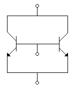
Discrete transistors T1 and T2 having maximum collector current rating of 0.75 amp are connected in parallel as shown in the figure, this combination is treated as a single transistor to carry a total current of 1 ampere, when biased with self bias circuit. When the circuit is switched on, T1 draws 0.55 amps and T2 draws 0.45 amps. If the supply is kept on continuously, ultimately it is very likely that
Detailed Solution for Test: Electronic Devices & Circuits - 3 - Question 18

T1 draws 0.55 A and T2 draws 0.45 A, T1 will get more heated and correct increase. Ultimately, I1 = 1A and I2 = 0.

Test: Electronic Devices & Circuits - 3 - Question 19

The number of p-n junctions in a semiconductor diode are

Detailed Solution for Test: Electronic Devices & Circuits - 3 - Question 19

Semiconductor diode has one p-n junction, BJT has two and SCR has three p-n junctions.

Test: Electronic Devices & Circuits - 3 - Question 20

Assertion (A): A high junction temperature may destroy a diode.

Reason (R): As temperature increases the reverse saturation current increases.

Detailed Solution for Test: Electronic Devices & Circuits - 3 - Question 20

Both A and R are correct. The diode is destroyed due to high reverse current.

Test: Electronic Devices & Circuits - 3 - Question 21

When a diode is not conducting, its bias is

Detailed Solution for Test: Electronic Devices & Circuits - 3 - Question 21

Diode conducts only when forward biased. There is no conduction when bias is zero or reverse.

Test: Electronic Devices & Circuits - 3 - Question 22

The SCR would be turned OFF by voltage reversal of applied anode-cathode ac supply of frequency of

Detailed Solution for Test: Electronic Devices & Circuits - 3 - Question 22

For inverter grade SCR, typical turn off time (toff) is 5 to 50 μsec while 50 to 100 μsec for converter grade SCR.

Hence supply frequency of 5 kHz will turn off the SCR by voltage reversal
because = 200 μsec.

Test: Electronic Devices & Circuits - 3 - Question 23

The number of valence electrons in a donor atom is

Detailed Solution for Test: Electronic Devices & Circuits - 3 - Question 23

Therefore, it can donate one electron.

Test: Electronic Devices & Circuits - 3 - Question 24

An electron rises through a voltage of 100 V. The energy acquired by it will be

Detailed Solution for Test: Electronic Devices & Circuits - 3 - Question 24

When an electron rises through 1 V, energy = 1 eV.

Test: Electronic Devices & Circuits - 3 - Question 25

Measurement of hall coefficient enables the determination of

Detailed Solution for Test: Electronic Devices & Circuits - 3 - Question 25

Hall effect can be used to find type and concentration of charge carriers.

Information about Test: Electronic Devices & Circuits - 3 Page
In this test you can find the Exam questions for Test: Electronic Devices & Circuits - 3 solved & explained in the simplest way possible. Besides giving Questions and answers for Test: Electronic Devices & Circuits - 3, EduRev gives you an ample number of Online tests for practice

Top Courses for Electrical Engineering (EE)

Download as PDF

Top Courses for Electrical Engineering (EE)