Electrical Engineering (EE) Exam  >  Electrical Engineering (EE) Tests  >  Test: Electronic Devices & Circuits - 4 - Electrical Engineering (EE) MCQ

Test: Electronic Devices & Circuits - 4 - Electrical Engineering (EE) MCQ


Test Description

25 Questions MCQ Test - Test: Electronic Devices & Circuits - 4

Test: Electronic Devices & Circuits - 4 for Electrical Engineering (EE) 2024 is part of Electrical Engineering (EE) preparation. The Test: Electronic Devices & Circuits - 4 questions and answers have been prepared according to the Electrical Engineering (EE) exam syllabus.The Test: Electronic Devices & Circuits - 4 MCQs are made for Electrical Engineering (EE) 2024 Exam. Find important definitions, questions, notes, meanings, examples, exercises, MCQs and online tests for Test: Electronic Devices & Circuits - 4 below.
Solutions of Test: Electronic Devices & Circuits - 4 questions in English are available as part of our course for Electrical Engineering (EE) & Test: Electronic Devices & Circuits - 4 solutions in Hindi for Electrical Engineering (EE) course. Download more important topics, notes, lectures and mock test series for Electrical Engineering (EE) Exam by signing up for free. Attempt Test: Electronic Devices & Circuits - 4 | 25 questions in 25 minutes | Mock test for Electrical Engineering (EE) preparation | Free important questions MCQ to study for Electrical Engineering (EE) Exam | Download free PDF with solutions
Test: Electronic Devices & Circuits - 4 - Question 1

An increase in junction temperature of a semiconductor diode

Detailed Solution for Test: Electronic Devices & Circuits - 4 - Question 1

Reverse saturation current doubles for every 10ºC rise in junction temperature.

Test: Electronic Devices & Circuits - 4 - Question 2

An air gap provided in the iron core of an inductor prevents

1 Crore+ students have signed up on EduRev. Have you? Download the App
Test: Electronic Devices & Circuits - 4 - Question 3

Generally, the gain of a transistor amplifier falls at high frequency due to the

Test: Electronic Devices & Circuits - 4 - Question 4

Which of these has a layer of intrinsic semiconductor?

Detailed Solution for Test: Electronic Devices & Circuits - 4 - Question 4

The intrinsic layer is in between p and n layers.

Test: Electronic Devices & Circuits - 4 - Question 5

Assertion (A): When Diode used as rectifier the reverse breakdown voltage should not be exceeded.

Reason (R): A high inverse voltage can destroy a p-n junction.

Detailed Solution for Test: Electronic Devices & Circuits - 4 - Question 5

PIV is an important parameter in rectifier operation.

Test: Electronic Devices & Circuits - 4 - Question 6

A Si sample is doped with a fixed number of group N impurities. The electron density n is measured from 4 K to 1200 k for the sample. Which one of the following is correct?

Test: Electronic Devices & Circuits - 4 - Question 7

Assertion (A): In design of circuit using BJT, a derating factor is used.

Reason (R): As the ambient temperature increases, heat dissipation becomes slower.

Detailed Solution for Test: Electronic Devices & Circuits - 4 - Question 7

Increase of ambient temperature lowers the heat dissipation capacity.

Therefore derated operation of BJT is necessary lest BJT should be destroyed.

Test: Electronic Devices & Circuits - 4 - Question 8

If the drift velocity of holes under a field gradient of 100 V/m is 5m/sec. Their mobility is

Detailed Solution for Test: Electronic Devices & Circuits - 4 - Question 8

E = μ . Vd μ =.

Test: Electronic Devices & Circuits - 4 - Question 9

In a P type silicon sample, the hole concentration is 2.25 x 10¹⁵ / cm3. If the intrinsic carrier concentration is 1.5 x 10¹⁰/ cm3 the electron concentration is

Detailed Solution for Test: Electronic Devices & Circuits - 4 - Question 9

Electron concentration .

Test: Electronic Devices & Circuits - 4 - Question 10

The behaviour of a JFET is similar to that of

Detailed Solution for Test: Electronic Devices & Circuits - 4 - Question 10

Both JFET and vacuum triode are voltage controlled devices.

Test: Electronic Devices & Circuits - 4 - Question 11

What is the effect of cut in voltage on the wave form of output as compared to input in a semiconductor diode?

Detailed Solution for Test: Electronic Devices & Circuits - 4 - Question 11

Since the duration of output waveform is less than 180º, output voltage is less than input voltage.

Test: Electronic Devices & Circuits - 4 - Question 12

As temperature increases the number of free electrons and holes in an intrinsic semiconductor

Detailed Solution for Test: Electronic Devices & Circuits - 4 - Question 12

Increase of temperature increases conductivity of semiconductors.

Test: Electronic Devices & Circuits - 4 - Question 13

At room temperature kT = 0.03 eV.

Test: Electronic Devices & Circuits - 4 - Question 14

Assertion (A): A JFET behaves as a resistor when VGS < VP.

Reason (R): When VGS < VP, the drain current in a JFET is almost constant.

Test: Electronic Devices & Circuits - 4 - Question 15

In a reverse biased P-N junction, the current through the junction increases abruptly at

Test: Electronic Devices & Circuits - 4 - Question 16

Dielectric strength of polythene is around

Test: Electronic Devices & Circuits - 4 - Question 17

Resistivity of hard drawn copper is

Test: Electronic Devices & Circuits - 4 - Question 18

The channel of JFET consists of

Detailed Solution for Test: Electronic Devices & Circuits - 4 - Question 18

The channel in JFET may be n type or p type. If channel is n type, gate is p type and if channel is p type gate is n type.

Test: Electronic Devices & Circuits - 4 - Question 19

In a bipolar junction transistor adc = 0.98, ICO= 2 μA and 1B = 15 μA. The collector current IC is

Detailed Solution for Test: Electronic Devices & Circuits - 4 - Question 19

Test: Electronic Devices & Circuits - 4 - Question 20

The voltage across the secondary of the transformer in a half wave rectifier with a shunt capacitor filter is 50 volts. The maximum voltage that will occur on the reverse biased diode will be

Test: Electronic Devices & Circuits - 4 - Question 21

Assertion (A): The forward resistance of a p-n diode is not constant.

Reason (R): The v-i characteristics of p-n diode is non-linear.

Detailed Solution for Test: Electronic Devices & Circuits - 4 - Question 21

If v-i characteristics is non linear, the ratio v-i is not constant.

Test: Electronic Devices & Circuits - 4 - Question 22

For a photoengraving the mask used is

Detailed Solution for Test: Electronic Devices & Circuits - 4 - Question 22

The mask that is prepared first is called the master mask made from glass substrates covered by thin chromium film.

From the master masks are prepared working masks by contact pointing and used for Photolithography which means Photo engraving.

Test: Electronic Devices & Circuits - 4 - Question 23

In a varactor diode the increase in width of depletion layer results in

Detailed Solution for Test: Electronic Devices & Circuits - 4 - Question 23

Capacitance is inversely proportional to distance between plates.

Test: Electronic Devices & Circuits - 4 - Question 24

In given figure a silicon diode is carrying a constant current of 1 mA. When the temperature of the diode is 20ºC, VD is found to be 700 mV. If the temperature rises to 40ºC, VD becomes approximately equal to
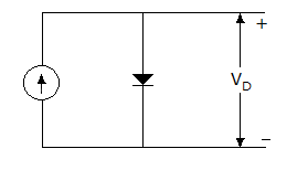
Detailed Solution for Test: Electronic Devices & Circuits - 4 - Question 24

Id = Io(eVD/ηVT - 1)

By considering , then

= eVD/ηVT

Id is constant according to question,

VD a T

.

Test: Electronic Devices & Circuits - 4 - Question 25

The work function of a photo surface whose threshold wave length is 1200 A, will be

Information about Test: Electronic Devices & Circuits - 4 Page
In this test you can find the Exam questions for Test: Electronic Devices & Circuits - 4 solved & explained in the simplest way possible. Besides giving Questions and answers for Test: Electronic Devices & Circuits - 4, EduRev gives you an ample number of Online tests for practice

Top Courses for Electrical Engineering (EE)

Download as PDF

Top Courses for Electrical Engineering (EE)