Index
All videos of Electronic Devices (Video Lectures) for Electronics and Communication Engineering (ECE) Exam
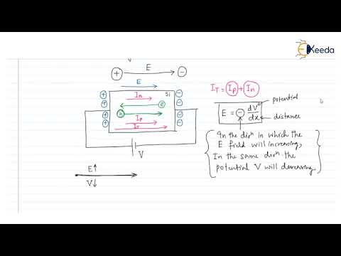
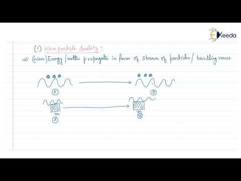
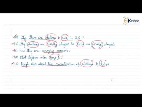
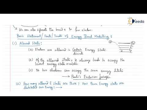
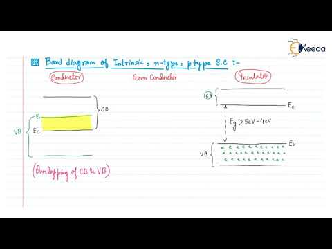
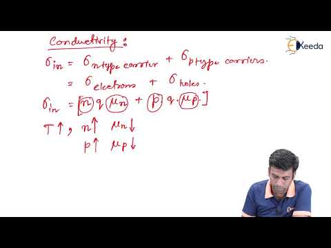
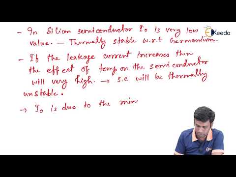
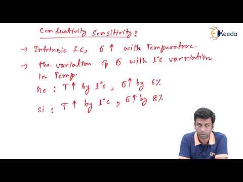
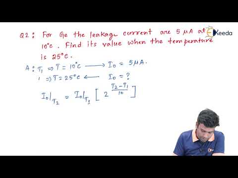
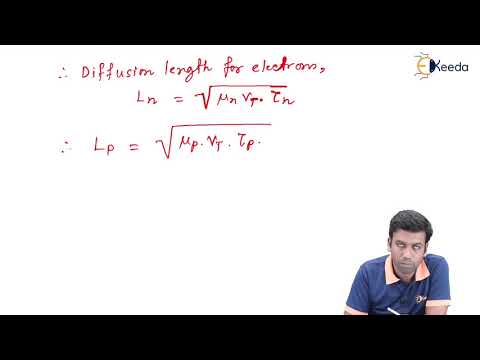
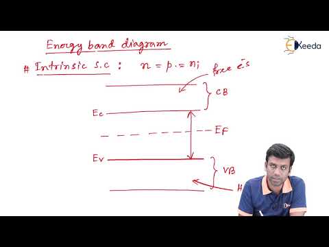
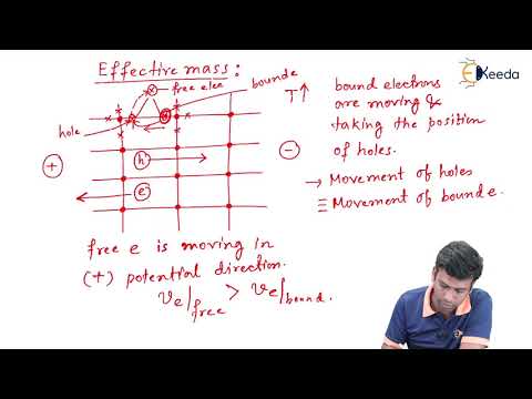
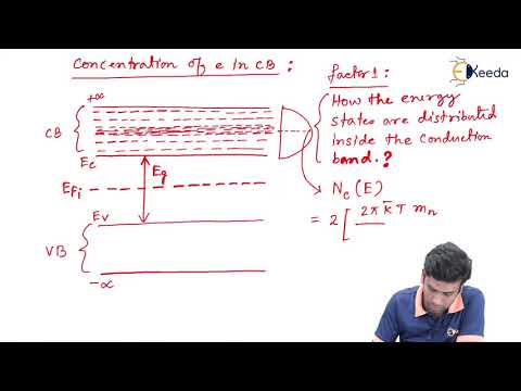
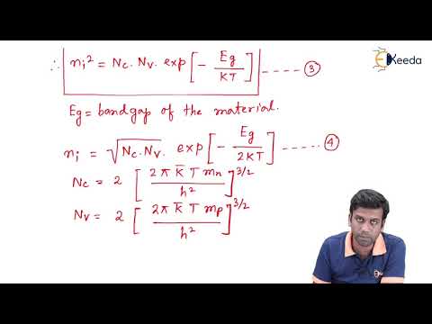
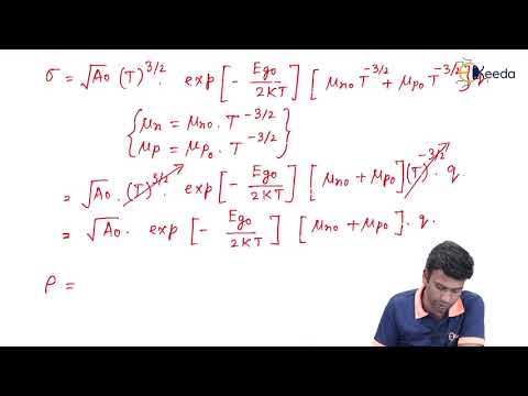
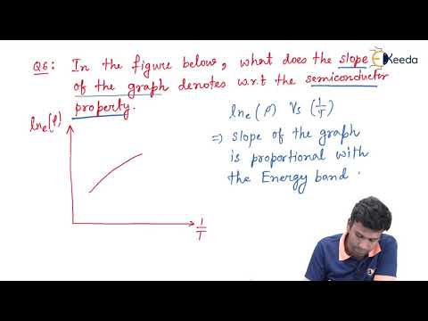
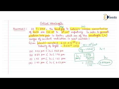
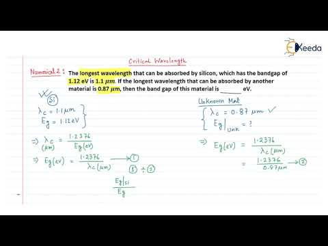
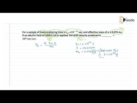
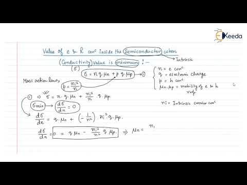
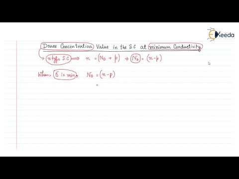
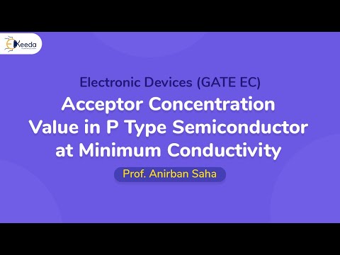
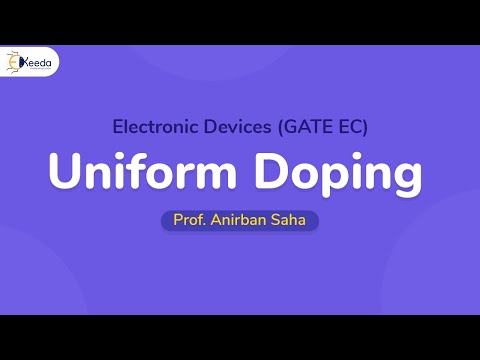
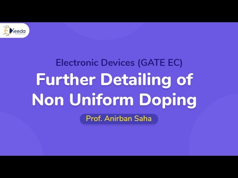
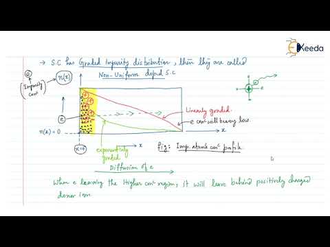
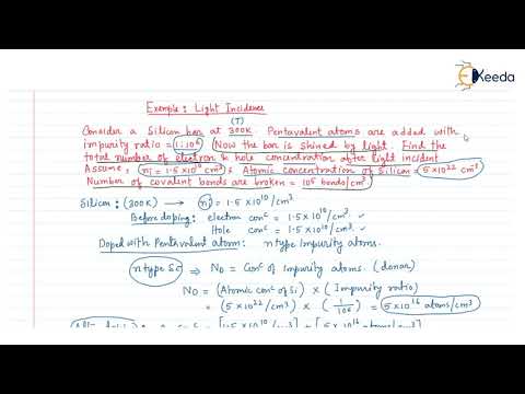
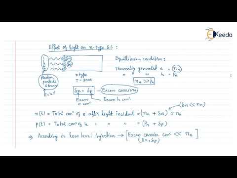
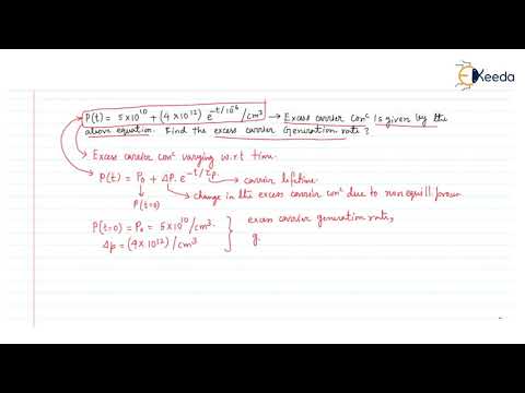
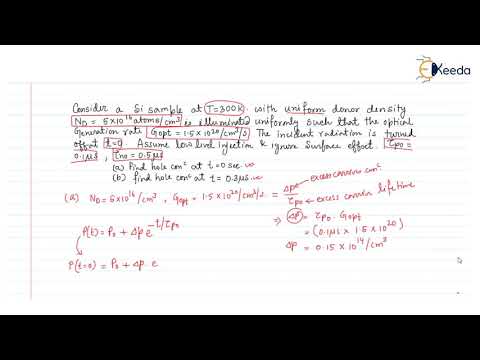
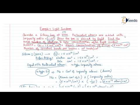
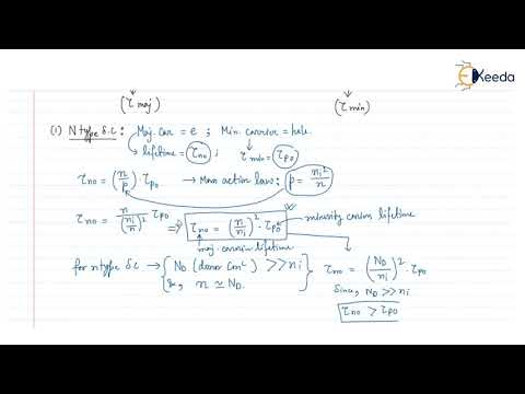
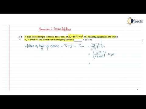
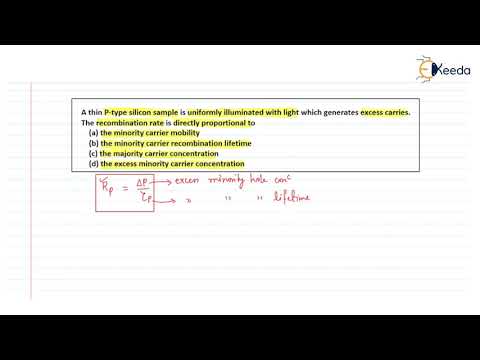
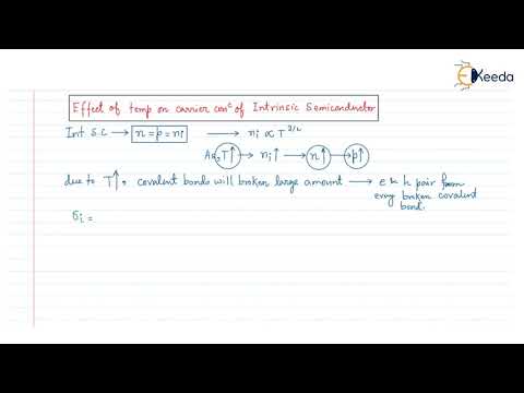
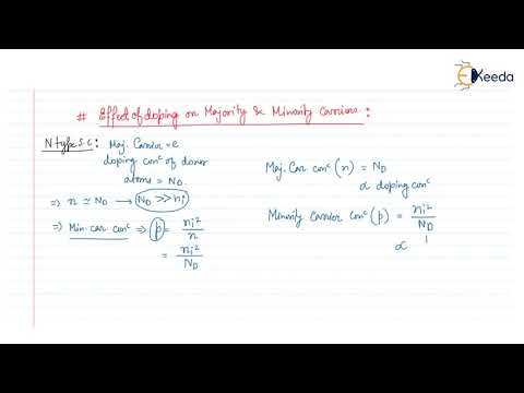
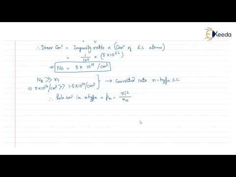
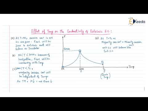
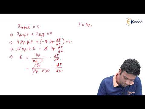
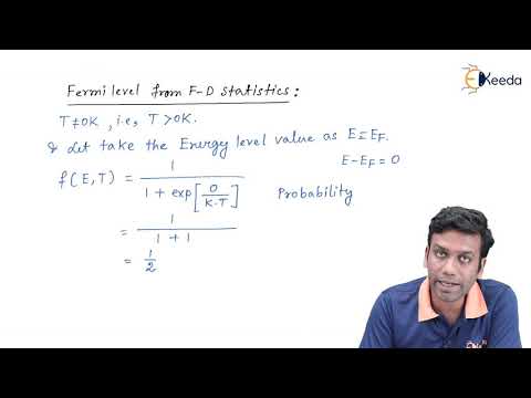
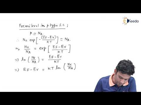
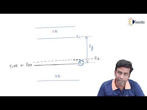
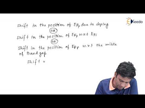
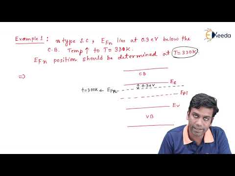
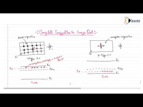
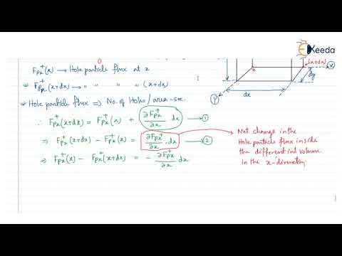
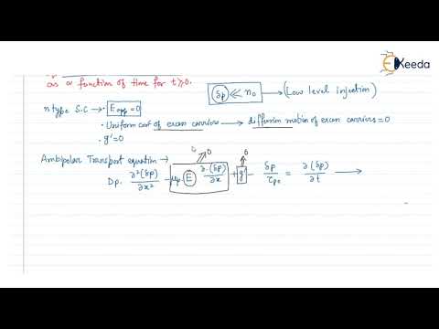
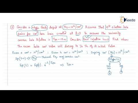
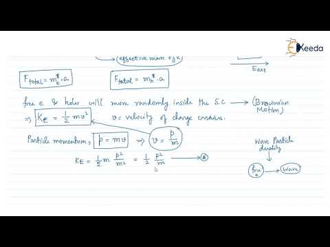
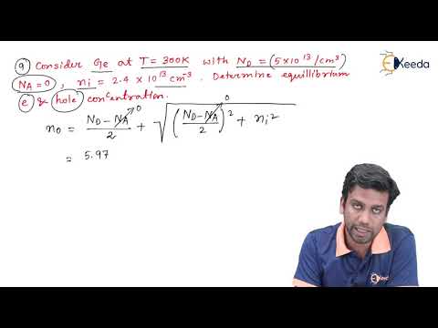
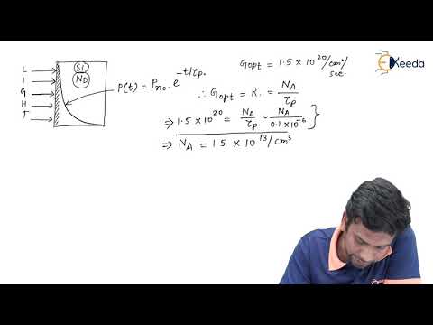
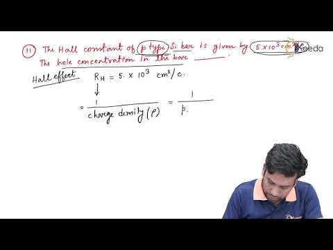
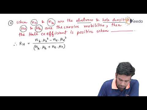
Semiconductors in Electronic Device
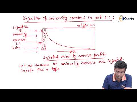


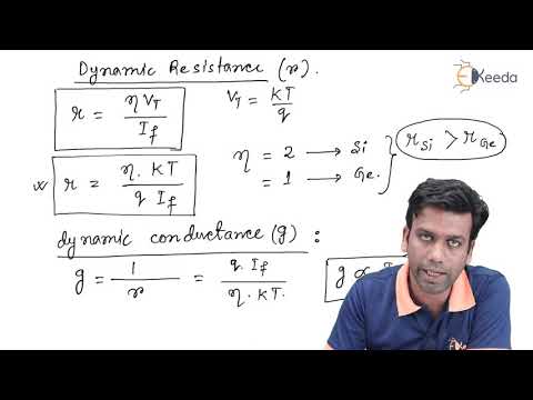
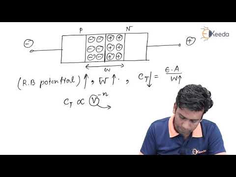
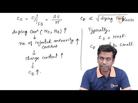
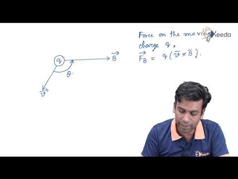
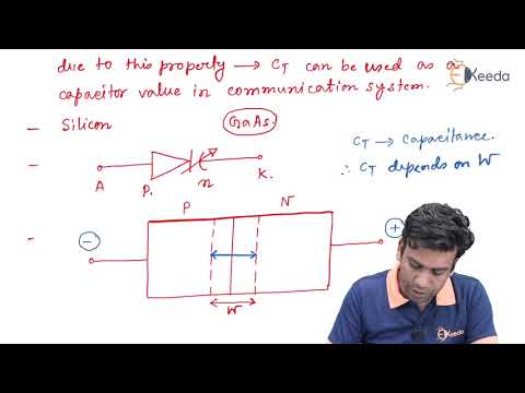
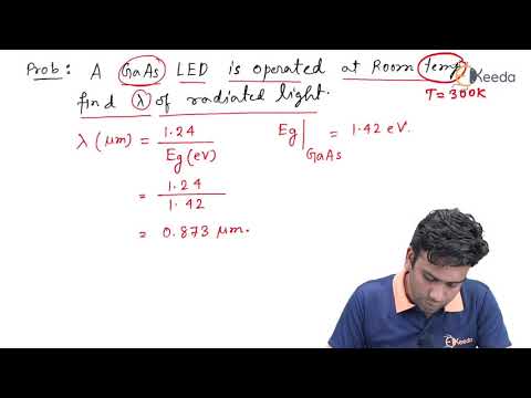
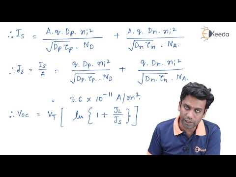
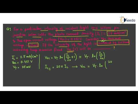
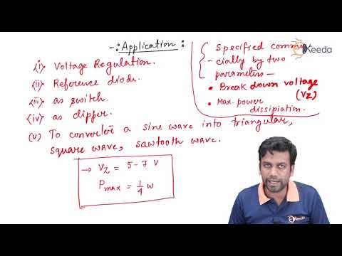
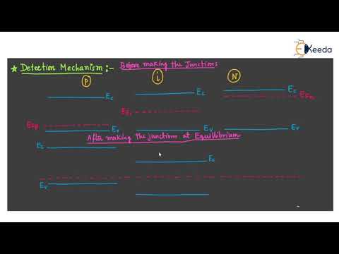
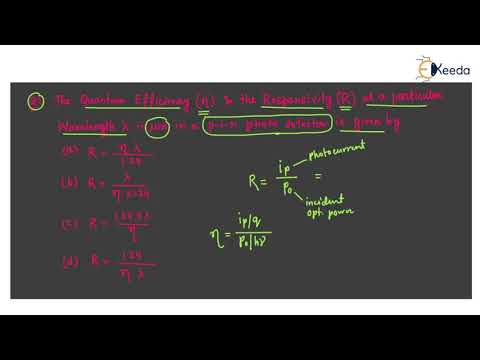
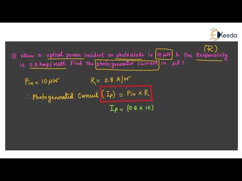
P-N Diodes


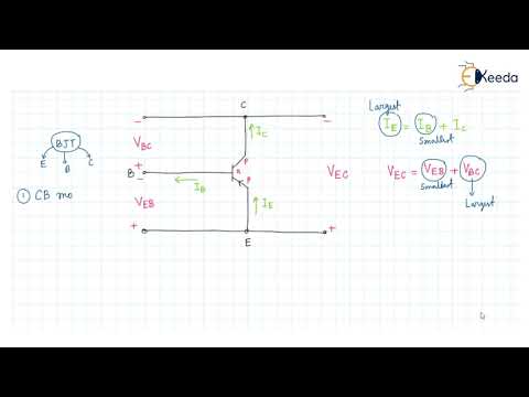
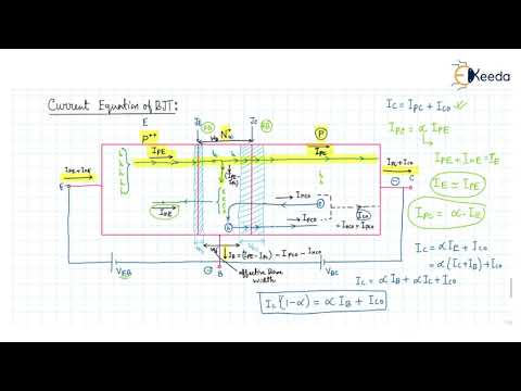
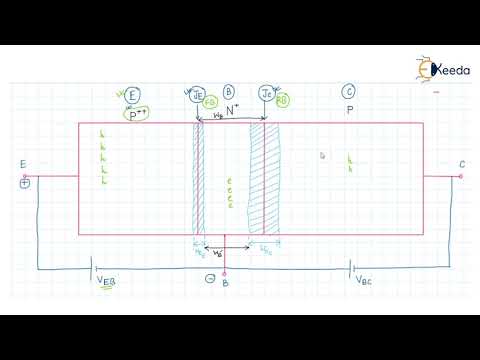
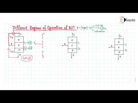
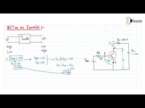
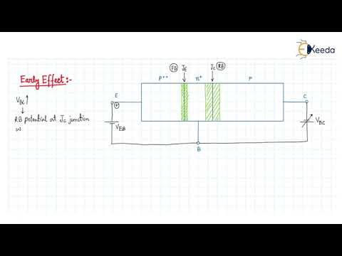
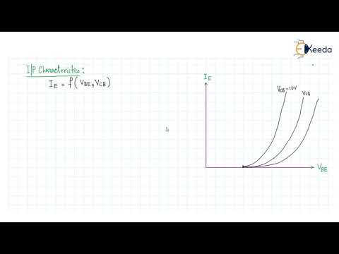
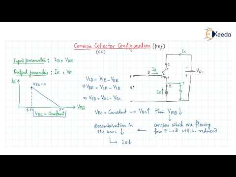
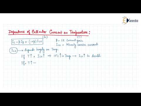
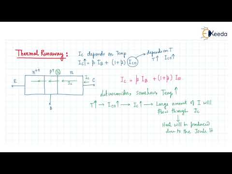
Bipolar Junction Transistor - BJT
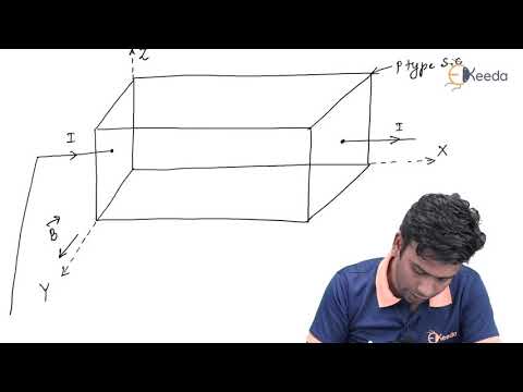
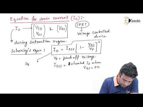
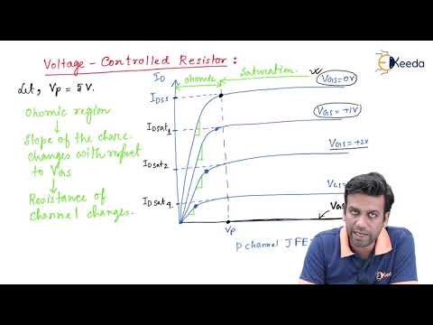
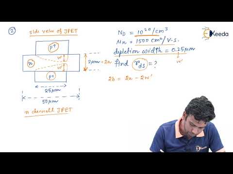
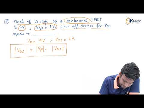
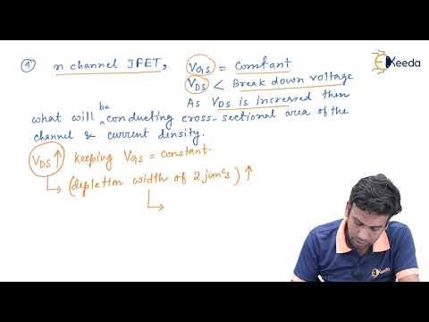
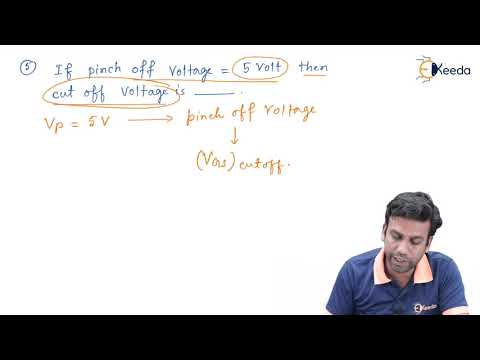
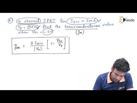
Junction Field Effect Transistor (JFET)
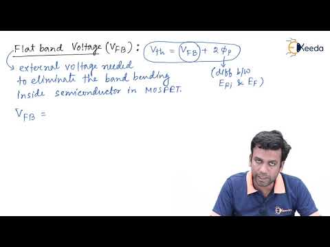
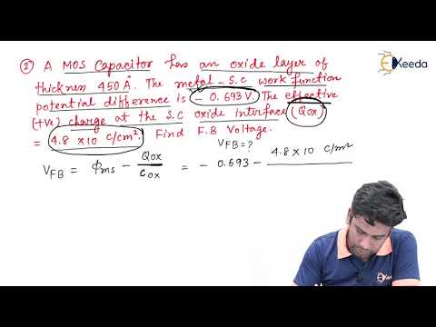
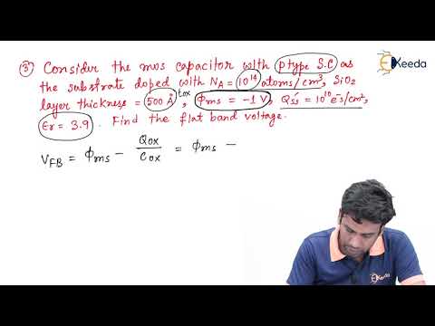
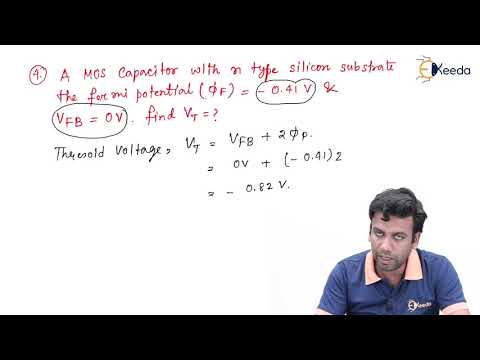
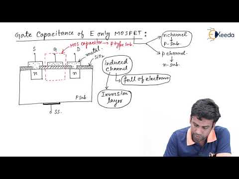
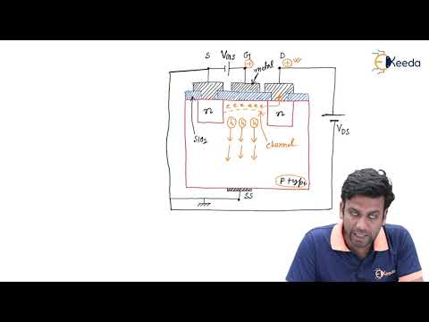
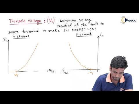
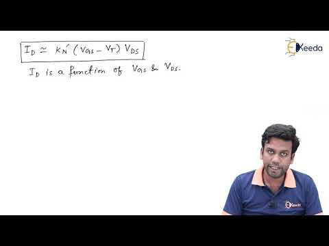
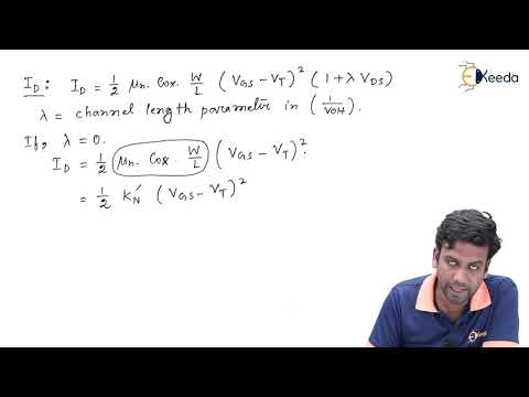
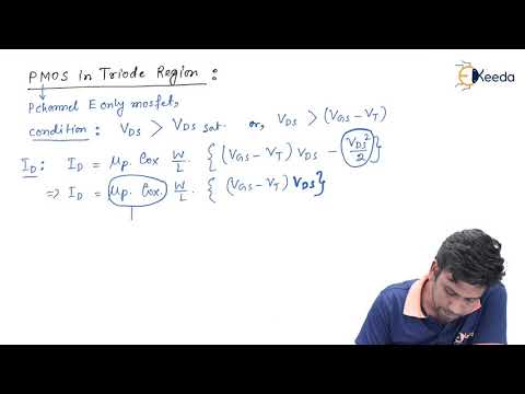
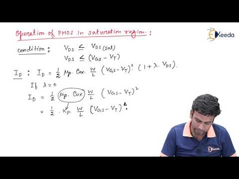
Metal Oxide Semiconductor Field Effect Transistor
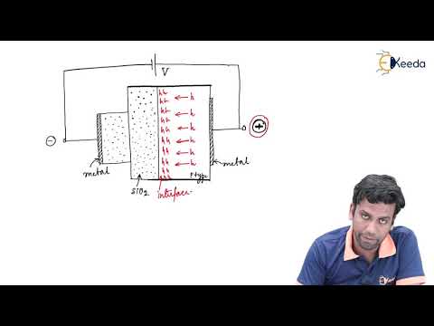
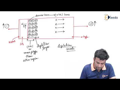


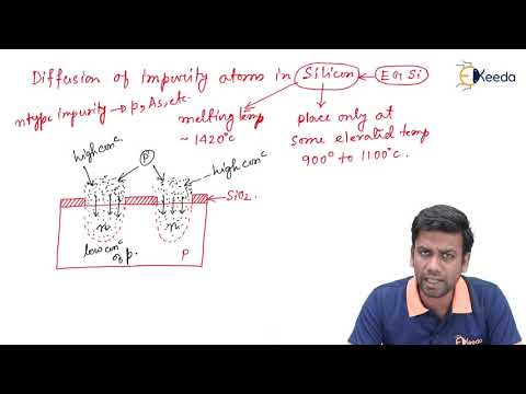
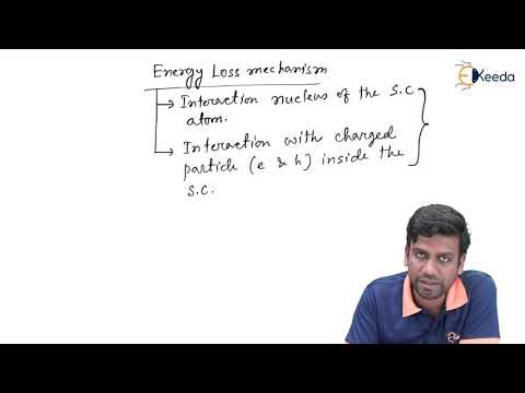
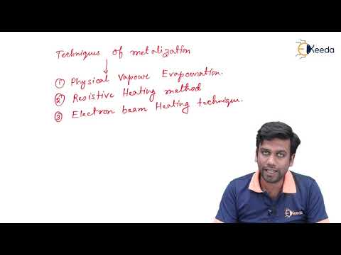
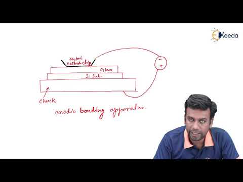
MOSFET Processing

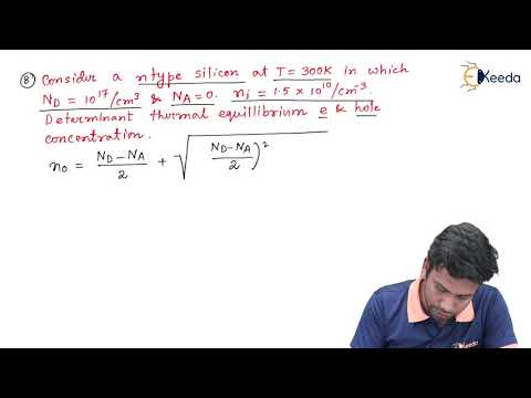
GATE Previous Year Questions (PYQ)


Video lectures for Electronic Devices (Video Lectures) 2025 is part of Electronics and Communication Engineering (ECE) exam preparation. The videos have been prepared according to the Electronics and Communication Engineering (ECE) exam syllabus. The Video lectures, notes, tests & MCQs are made for Electronics and Communication Engineering (ECE) 2025 Exam. Find important definitions, questions, notes, meanings, examples, exercises, MCQs and online tests here.
Video lectures of Electronic Devices (Video Lectures) in English & Hindi are available as part of Electronics and Communication Engineering (ECE) exam.
Download more important topics, notes, lectures and mock test series for Electronics and Communication Engineering (ECE) Exam by signing up for free.
|
© EduRev
|
Education Revolution
|


|


Signup to see your scores
go up within 7 days!
Access 1000+ FREE Docs, Videos and Tests
Takes less than 10 seconds to signup