


All Exams > Electrical Engineering (EE) > 6 Months Preparation for GATE Electrical > All Questions
All questions of Transistors for Electrical Engineering (EE) Exam
The transfer of a signal in a transistor is_________- a)low to high resistance
- b)high to low resistance
- c)collector to base junction
- d)emitter to base junction
Correct answer is option 'A'. Can you explain this answer?
The transfer of a signal in a transistor is_________
a)
low to high resistance
b)
high to low resistance
c)
collector to base junction
d)
emitter to base junction
 | Bhaskar Joshi answered |
A forward biased emitter base junction has a low resistance path. A reversed biased junction has a high resistance path. The weak signal is introduced in a low resistance circuit and the output is taken from the high resistance circuit.

The advantages over the vacuum triode for a junction transistor is_________- a)high power consumption
- b)high efficiency
- c)large size
- d)less doping
Correct answer is option 'B'. Can you explain this answer?
The advantages over the vacuum triode for a junction transistor is_________
a)
high power consumption
b)
high efficiency
c)
large size
d)
less doping
 | Swara Dasgupta answered |
A junction transistor is an analogous to a vacuum triode. The main difference between them is that a transistor is a current device while a vacuum triode is a voltage device. The advantages of a transistor over a vacuum triode are long life, high efficiency, light weight, smaller in size, less power consumption.
The base current amplification factor β is given by_________- a)IC/IB
- b)IB/IC
- c)IE/IB
- d)IB/IE
Correct answer is option 'A'. Can you explain this answer?
The base current amplification factor β is given by_________
a)
IC/IB
b)
IB/IC
c)
IE/IB
d)
IB/IE
| | Niharika Basu answered |
The current amplification factor (β) is given by IC//IB. When no signal is applied, then the ratio of collector current to the base current is called current amplification factor of a transistor.
In CB configuration, the value of α=0.98A. A voltage drop of 4.9V is obtained across the resistor of 5KΩ when connected in collector circuit. Find the base current.- a)0.01mA
- b)0.07mA
- c)0.02mA
- d)0.05mA
Correct answer is option 'C'. Can you explain this answer?
In CB configuration, the value of α=0.98A. A voltage drop of 4.9V is obtained across the resistor of 5KΩ when connected in collector circuit. Find the base current.
a)
0.01mA
b)
0.07mA
c)
0.02mA
d)
0.05mA
 | Sagnik Sen answered |
Here, IC=4.9/5K=0.98mA
α = IC/IE .So,
IE=IC/α=0.98/0.98=1mA.
IB=IE-IC=1-0.98=0.02Ma.
α = IC/IE .So,
IE=IC/α=0.98/0.98=1mA.
IB=IE-IC=1-0.98=0.02Ma.
Which of the following are true for a PNP transistor?- a)the emitter current is less than the collector current
- b)the collector current is less than the emitter current
- c)the electrons are majority charge carriers
- d)the holes are the minority charge carriers
Correct answer is option 'B'. Can you explain this answer?
Which of the following are true for a PNP transistor?
a)
the emitter current is less than the collector current
b)
the collector current is less than the emitter current
c)
the electrons are majority charge carriers
d)
the holes are the minority charge carriers
 | Bijoy Mehra answered |
The 2 – 5% of holes is lost in recombination with electrons in the base region. The majority charge carriers are holes for a PNP transistor. Thus the collector current is slightly less than the emitter current.
The negative sign in the formula of amplification factor indicates_________- a)that IE flows into transistor while IC flows out it
- b)that IC flows into transistor while IE flows out it
- c)that IB flows into transistor while IC flows out it
- d) that IC flows into transistor while IB flows out it
Correct answer is option 'A'. Can you explain this answer?
The negative sign in the formula of amplification factor indicates_________
a)
that IE flows into transistor while IC flows out it
b)
that IC flows into transistor while IE flows out it
c)
that IB flows into transistor while IC flows out it
d)
that IC flows into transistor while IB flows out it
 | Anushka Bose answered |
When no signal is applied, the ratio of collector current to emitter current is called dc alpha, αdc of a transistor. αdc=-IC/IE. It is the measure of the quality of a transistor. Higher is the value of α, better is the transistor in the sense that collector current approaches the emitter current.
Determine the value of emitter current and collector current of a transistor having α=0.98 and collector to base leakage current ICBO=4µA. The base current is 50µA.- a)1.5mA
- b)3.7mA
- c)2.7mA
- d)4.5mA
Correct answer is option 'C'. Can you explain this answer?
Determine the value of emitter current and collector current of a transistor having α=0.98 and collector to base leakage current ICBO=4µA. The base current is 50µA.
a)
1.5mA
b)
3.7mA
c)
2.7mA
d)
4.5mA
| | Anushka Bose answered |
Given, IB=50µA=0.05mA
ICBO=4µA=0.004Ma
IC=α/(1- α)IB+1/(1- α)ICBO=2.45+0.2=2.65Ma
IE=IC+IB=2.65+0.05=2.7mA.
ICBO=4µA=0.004Ma
IC=α/(1- α)IB+1/(1- α)ICBO=2.45+0.2=2.65Ma
IE=IC+IB=2.65+0.05=2.7mA.
In the saturated region, the transistor acts like a_________- a)poor transistor
- b)amplifier
- c)open switch
- d)closed switch
Correct answer is option 'D'. Can you explain this answer?
In the saturated region, the transistor acts like a_________
a)
poor transistor
b)
amplifier
c)
open switch
d)
closed switch
| | Kalyan Patel answered |
In this mode, both the junctions are forward biased. The negative terminal of the battery is connected to the emitter. The collector current becomes independent of base current. In this mode the transistor acts as a closed switch.
The current amplification factor ϒdc is given by_________- a)IE/IB
- b)IB/IE
- c)IC/IE
- d) IE/IC
Correct answer is option 'A'. Can you explain this answer?
The current amplification factor ϒdc is given by_________
a)
IE/IB
b)
IB/IE
c)
IC/IE
d)
IE/IC
 | Subhankar Malik answered |
When no signal is applied, then the ratio of emitter current to base current is called as ϒdc of the transistor. As the collector is common to both input and output circuits, hence the name common collector configuration.
If the emitter-base junction is forward biased and the collector-base junction is reverse biased, what will be the region of operation for a transistor?- a)cut off region
- b)saturated region
- c)inverted region
- d)active region
Correct answer is option 'D'. Can you explain this answer?
If the emitter-base junction is forward biased and the collector-base junction is reverse biased, what will be the region of operation for a transistor?
a)
cut off region
b)
saturated region
c)
inverted region
d)
active region
| | Bijoy Nair answered |
Region of Operation for a Transistor
The region of operation for a transistor refers to the operating mode in which the transistor functions. These modes are determined by the biasing conditions applied to the emitter-base and collector-base junctions of the transistor. In this case, the emitter-base junction is forward biased, and the collector-base junction is reverse biased. This biasing arrangement corresponds to the active region of operation for a transistor.
1. Cut-off Region
- In the cut-off region, both the emitter-base and collector-base junctions are reverse biased.
- No current flows through the transistor, and it acts as an open circuit.
- The transistor is completely turned off, and no amplification or switching action occurs.
2. Saturated Region
- In the saturated region, both the emitter-base and collector-base junctions are forward biased.
- The transistor is fully turned on, allowing a large current to flow through it.
- It acts as a closed switch, with a low resistance between the collector and emitter.
- This region is commonly used in digital logic circuits and switching applications.
3. Inverted Region
- The inverted region is not a recognized region of operation for a transistor.
- It may refer to a situation where the polarity of the voltage applied to the emitter-base and collector-base junctions is reversed.
- This condition can damage the transistor and is not desirable in normal operation.
4. Active Region
- In the active region, the emitter-base junction is forward biased, and the collector-base junction is reverse biased.
- The transistor operates as an amplifier, allowing a small input current or voltage to control a larger output current or voltage.
- It is the most common region of operation for transistors in analog circuits.
- The active region enables amplification, signal processing, and other functions in electronic circuits.
Therefore, in the given biasing arrangement, where the emitter-base junction is forward biased, and the collector-base junction is reverse biased, the transistor operates in the active region.
The application of a CC configured transistor is_________- a)voltage multiplier
- b)level shifter
- c)rectification
- d)impedance matching
Correct answer is option 'D'. Can you explain this answer?
The application of a CC configured transistor is_________
a)
voltage multiplier
b)
level shifter
c)
rectification
d)
impedance matching
 | Milan Saha answered |
The most important use of CC transistor is an impedance matching device. It is seldom used for amplification purposes. The current gain is same as that of CE configured transistor.
The point on the DC load line which is represented by ‘Q’ is called _________- a)cut off point
- b)cut in point
- c)breakdown point
- d)operating point
Correct answer is option 'D'. Can you explain this answer?
The point on the DC load line which is represented by ‘Q’ is called _________
a)
cut off point
b)
cut in point
c)
breakdown point
d)
operating point
 | Rutuja Deshpande answered |
The point which represents the values of IC and VCE that exist in a transistor circuit when no signal is applied is called as operating point. This is also called as working point or quiescent point.
The value of αac for all practical purposes, for commercial transistors range from_________- a)0.5-0.6
- b)0.7-0.77
- c)0.8-0.88
- d)0.9-0.99
Correct answer is option 'D'. Can you explain this answer?
The value of αac for all practical purposes, for commercial transistors range from_________
a)
0.5-0.6
b)
0.7-0.77
c)
0.8-0.88
d)
0.9-0.99
| | Arshiya Basu answered |
Range of αac for Commercial Transistors
The value of αac (common base current gain) for commercial transistors typically falls within the range of 0.9-0.99. This parameter is crucial in determining the amplification capabilities of the transistor in AC signal applications.
Importance of αac
- αac represents the ratio of the change in collector current to the change in base current in an AC signal scenario.
- It indicates how effectively the transistor can amplify small AC signals.
Practical Considerations
- Commercial transistors are designed and optimized to have high values of αac to ensure efficient signal amplification.
- Values in the range of 0.9-0.99 indicate that the transistor can provide significant amplification of AC signals.
Impact on Circuit Design
- Engineers rely on the specified αac value when designing circuits to ensure proper signal amplification and stability.
- A high αac value allows for greater control over the amplification factor in a circuit.
Conclusion
In conclusion, the range of 0.9-0.99 for αac in commercial transistors signifies their ability to effectively amplify AC signals in practical applications. This parameter plays a crucial role in circuit design and performance, making it a key consideration for engineers working with transistors.
The relation between α and β is_________- a)β = α/ (1-α)
- b)α = β/(1+β)
- c)β = α/ (1+α)
- d)α = β/(1- β)
Correct answer is option 'B'. Can you explain this answer?
The relation between α and β is_________
a)
β = α/ (1-α)
b)
α = β/(1+β)
c)
β = α/ (1+α)
d)
α = β/(1- β)
| | Srestha Kumar answered |
The relation between two or more things refers to how they are connected or how they interact with each other. It can describe a cause-and-effect relationship, a correlation, a comparison, or any other type of connection between the things being considered. Relations can be positive or negative, strong or weak, direct or indirect, and can vary in intensity or significance. Understanding the relation between different factors or variables is important in fields such as science, mathematics, sociology, and many others, as it helps to explain patterns, predict outcomes, and make informed decisions.
In an NPN silicon transistor, α=0.995, IE=10mA and leakage current ICBO=0.5µA. Determine ICEO.- a)10µA
- b)100µA
- c)90µA
- d)500µA
Correct answer is option 'B'. Can you explain this answer?
In an NPN silicon transistor, α=0.995, IE=10mA and leakage current ICBO=0.5µA. Determine ICEO.
a)
10µA
b)
100µA
c)
90µA
d)
500µA
 | Asha Nambiar answered |
IC=α IE +ICBO =0.995*10mA+0.5µA=9.9505mA.
IB=IE-IC=10-9.9505=0.0495mA. β=α/(1-α)=0.995/(1-0.995)=199
ICEO=9.9505-199*0.0495=0.1mA==100µA.
IB=IE-IC=10-9.9505=0.0495mA. β=α/(1-α)=0.995/(1-0.995)=199
ICEO=9.9505-199*0.0495=0.1mA==100µA.
The base emitter voltage in a cut off region is_________- a)greater than 0.7V
- b)equal to 0.7V
- c)less than 0.7V
- d)cannot be predicted
Correct answer is option 'C'. Can you explain this answer?
The base emitter voltage in a cut off region is_________
a)
greater than 0.7V
b)
equal to 0.7V
c)
less than 0.7V
d)
cannot be predicted
| | Avantika Kaur answered |
The base-emitter voltage in the cutoff region of a transistor is less than 0.7V.
Explanation:
When a transistor is operating in the cutoff region, it means that there is no current flowing through it. In this state, both the base-emitter junction and the base-collector junction are reverse biased.
In the cutoff region, the base-emitter voltage (Vbe) is less than 0.7V. This is because the reverse bias voltage applied to the base-emitter junction prevents the flow of current through it. The exact value of Vbe in the cutoff region depends on the characteristics of the transistor and the specific circuit conditions.
The cutoff region is characterized by the following conditions:
1. Base current (Ib) is very close to zero.
2. Collector current (Ic) is zero.
3. Base-emitter voltage (Vbe) is less than 0.7V.
In the cutoff region, the transistor acts as an open switch. It does not amplify any signals and does not allow the flow of current from the collector to the emitter.
It is important to note that the cutoff region is one of the three main operating regions of a transistor, along with the active region and saturation region. In the active region, the transistor operates as an amplifier, while in the saturation region, it acts as a closed switch.
In summary, the base-emitter voltage in the cutoff region of a transistor is less than 0.7V. This is because the transistor is in a state where no current flows through it due to the reverse bias applied to the base-emitter junction.
A germanium transistor with α=0.98 gives a reverse saturation current ICBO=10µA in a CB configuration. When it is used in CE configuration with a base current of 0.22µA, calculate the collector current.- a)0.9867mA
- b)0.7654mA
- c)0.51078mA
- d)0.23456mA
Correct answer is option 'C'. Can you explain this answer?
A germanium transistor with α=0.98 gives a reverse saturation current ICBO=10µA in a CB configuration. When it is used in CE configuration with a base current of 0.22µA, calculate the collector current.
a)
0.9867mA
b)
0.7654mA
c)
0.51078mA
d)
0.23456mA
| | Asha Nambiar answered |
Given, ICBO=10µA, α=0.98 and IB =0.22µA. IC=α/ (1-α) IB+ 1/(1-α) ICBO
0.01078+0.5=0.51078mA.
0.01078+0.5=0.51078mA.
The CC configuration has an input resistance_________- a)500kΩ
- b)750kΩ
- c)600kΩ
- d)400kΩ
Correct answer is option 'B'. Can you explain this answer?
The CC configuration has an input resistance_________
a)
500kΩ
b)
750kΩ
c)
600kΩ
d)
400kΩ
| | Subhankar Malik answered |
It has a high input resistance and very low output resistance so the voltage gain is always less one. It is used for driving a low impedance load from a high impedance source.
Which of the following statements is true?- a)Solid state switches are applications for an AC output
- b)LED’s can be driven by transistor logics
- c)Only NPN transistor can be used as a switch
- d)Transistor operates as a switch only in active region
Correct answer is option 'B'. Can you explain this answer?
Which of the following statements is true?
a)
Solid state switches are applications for an AC output
b)
LED’s can be driven by transistor logics
c)
Only NPN transistor can be used as a switch
d)
Transistor operates as a switch only in active region
 | Shreya Choudhary answered |
Output devices like LED’s only require a few milliamps at logic level DC voltages and can therefore be driven directly by the output of a logic gate. However, high power devices such as motors or lamps require more power than that supplied by an ordinary logic gate so transistor switches are used.
The switching of power with a NPN transistor is called_________- a)sourcing current
- b)sinking current
- c)forward sourcing
- d)reverse sinking
Correct answer is option 'B'. Can you explain this answer?
The switching of power with a NPN transistor is called_________
a)
sourcing current
b)
sinking current
c)
forward sourcing
d)
reverse sinking
| | Nandita Kulkarni answered |
The switching of power with a NPN transistor is called sinking current.
NPN transistors are commonly used in electronic circuits to switch and control power. They have three layers of semiconductor material - the emitter, base, and collector. The emitter is negatively charged, the base is neutral, and the collector is positively charged.
When a positive voltage is applied to the base of an NPN transistor, it allows current to flow from the emitter to the collector. This is known as the "forward bias" state. Conversely, when the base voltage is lower than the emitter voltage, the transistor is in the "reverse bias" state and does not allow current to flow.
Sinking current:
Sinking current refers to the ability of a transistor to handle or control the flow of current from the collector to ground, or in other words, to "sink" current. In this configuration, the transistor acts as a switch or a current sink, allowing current to flow from the load to ground when it is turned on.
When the base-emitter junction is forward-biased, a small base current can control a much larger collector current flow. This allows the transistor to switch on and off a high-power load connected to the collector terminal. The collector-emitter voltage drop in this state is typically low, resulting in minimal power dissipation and efficient switching.
Advantages of sinking current:
1. Power control: Sinking current allows efficient control of high-power devices such as motors, solenoids, or relays, as it can handle larger current flows.
2. Protection: By connecting the load to the collector terminal, sinking current provides protection to the control circuitry from high voltages or inductive kickback generated by the load.
3. Flexibility: Sinking current allows multiple loads to be controlled by a single transistor, making it a versatile choice in various applications.
Overall, sinking current with an NPN transistor provides a reliable and efficient method of controlling power in electronic circuits. By utilizing the transistor's ability to sink current, it enables the safe and efficient switching of high-power devices.
What is the left hand section of a junction transistor called?- a)base
- b)collector
- c)emitter
- d)depletion region
Correct answer is option 'C'. Can you explain this answer?
What is the left hand section of a junction transistor called?
a)
base
b)
collector
c)
emitter
d)
depletion region
 | Diya Patel answered |
The main function of this section is to supply majority charge carriers to the base. Hence it is more heavily doped in comparison to other regions. This forms the left hand section of the transistor.
In ICEO, wt does the subscript ‘CEO’ mean?- a)collector to base emitter open
- b)emitter to base collector open
- c)collector to emitter base open
- d)emitter to collector base open
Correct answer is option 'C'. Can you explain this answer?
In ICEO, wt does the subscript ‘CEO’ mean?
a)
collector to base emitter open
b)
emitter to base collector open
c)
collector to emitter base open
d)
emitter to collector base open
| | Om Saini answered |
The subscript in ICEO refers to the "inception to effective date" of an insurance policy. It indicates the period of time between when the policy was initiated or created (inception) and when it becomes effective. This is important for determining the coverage start date and any waiting periods that may apply.
The base emitter voltage in a saturation region is_________- a)greater than 0.7V
- b)equal to 0.7V
- c)less than 0.7V
- d)cannot be predicted
Correct answer is option 'D'. Can you explain this answer?
The base emitter voltage in a saturation region is_________
a)
greater than 0.7V
b)
equal to 0.7V
c)
less than 0.7V
d)
cannot be predicted
 | Diya Ahuja answered |
From the saturation mode characteristics, the transistor acts as a single pole single throw solid state switch. A zero collector current flows. With a positive signal applied to the base of transistor it turns on like a closed switch.
When is the transistor said to be saturated?- a) when VCE is very low
- b)when VCE is very high
- c)when VBE is very low
- d)when VBE is very high
Correct answer is option 'A'. Can you explain this answer?
When is the transistor said to be saturated?
a)
when VCE is very low
b)
when VCE is very high
c)
when VBE is very low
d)
when VBE is very high
| | Pallavi Nair answered |
Transistor Saturation
Introduction:
The transistor is a three-layer semiconductor device that can amplify or switch electronic signals and electrical power. It consists of a collector (C), a base (B), and an emitter (E). The transistor operates in three regions: active, saturation, and cutoff. In the saturation region, the transistor is fully turned on and acts as a closed switch.
Definition:
Transistor saturation occurs when the transistor is biased in such a way that both the base-emitter junction (VBE) and the base-collector junction (VCE) are forward biased. This allows a significant current to flow through the collector-emitter path.
Explanation:
Transistor saturation is primarily determined by the voltages applied to the VBE and VCE junctions. When VBE is very low, it means that the base-emitter junction is forward biased with a small voltage. In this condition, the transistor is not in saturation because the base-emitter junction is not sufficiently forward biased to allow a large current to flow.
However, when VCE is very low, it means that the base-collector junction is forward biased with a small voltage. This condition allows a large current to flow through the collector-emitter path, and the transistor enters saturation. In saturation, the transistor acts as a closed switch, allowing maximum current to flow from the collector to the emitter.
Significance of VCE:
The voltage VCE is crucial in determining the saturation state of a transistor. When VCE is low, the transistor is in saturation, and it can be used as a switch to control other circuit elements. On the other hand, when VCE is high, the transistor is in the active region, and it can be used for amplification purposes.
Conclusion:
In summary, the transistor is said to be saturated when VCE is very low. This is because a low VCE voltage indicates that the base-collector junction is forward biased, allowing a large current to flow through the collector-emitter path. Understanding the saturation region is important for designing and analyzing transistor circuits for various applications.
In the operation of an NPN transistor, the electrons cross which region?- a)emitter region
- b)the region where there is high depletion
- c)the region where there is low depletion
- d)P type base region
Correct answer is option 'D'. Can you explain this answer?
In the operation of an NPN transistor, the electrons cross which region?
a)
emitter region
b)
the region where there is high depletion
c)
the region where there is low depletion
d)
P type base region
| | Jaya Yadav answered |
The electrons in the emitter region are repelled by the negative terminal of the battery towards the emitter junction. The potential barrier at the junction is reduced due to forward bias and base region is very thin and lightly doped, electrons cross the P type base region.
The range of β is _________- a)20 to 500
- b)50 to 300
- c)30 to 400
- d)10 to 20
Correct answer is option 'A'. Can you explain this answer?
The range of β is _________
a)
20 to 500
b)
50 to 300
c)
30 to 400
d)
10 to 20
 | Rutuja Pillai answered |
Almost in all the transistors, the base current is less than 5% of the emitter current. Due to this fact, it is generally greater than 20. Usually it ranges from 20 to 500. Hence this configuration is frequently used when appreciable current gain as well as voltage gain is required.
What is the output resistance of CC transistor?- a)25 Ω
- b)50 Ω
- c)100 Ω
- d)150 Ω
Correct answer is option 'A'. Can you explain this answer?
What is the output resistance of CC transistor?
a)
25 Ω
b)
50 Ω
c)
100 Ω
d)
150 Ω
 | Subhankar Ghoshal answered |
The CC transistor has a very low value of output resistance of 25 Ω. The voltage gain is always less one. It is used for driving a low impedance load from a high impedance source.
A transistor is connected in CE configuration. Collector supply voltage Vcc=10V, RL=800Ω, voltage drop across RL=0.8V, α=0.96. What is base current?- a)41.97µA
- b)56.78µA
- c)67.67µA
- d)78.54µA
Correct answer is option 'A'. Can you explain this answer?
A transistor is connected in CE configuration. Collector supply voltage Vcc=10V, RL=800Ω, voltage drop across RL=0.8V, α=0.96. What is base current?
a)
41.97µA
b)
56.78µA
c)
67.67µA
d)
78.54µA
 | Varun Banerjee answered |
Here, IC=0.8/800=1mA
β= α/ (1-α)=0.96/1-0.96=24.
Now, IB=IC/ β=1/24=41.67µA.
β= α/ (1-α)=0.96/1-0.96=24.
Now, IB=IC/ β=1/24=41.67µA.
When does the transistor act like an open switch?- a)cut off region
- b)inverted region
- c)saturated region
- d)active region
Correct answer is option 'A'. Can you explain this answer?
When does the transistor act like an open switch?
a)
cut off region
b)
inverted region
c)
saturated region
d)
active region
 | Rounak Choudhary answered |
In cut off region, both the junctions are reverse biased. The transistor has practically zero current because the emitter does not emit charge carriers to the base. So, the transistor acts as open switch.
The collector supply voltage for a CE configured transistor is 10V. The resistance RL=800Ω. The voltage drop across RL is 0.8V. Find the value of collector emitter voltage.- a)3.7V
- b)9.2V
- c)6.5V
- d)9.8V
Correct answer is option 'B'. Can you explain this answer?
The collector supply voltage for a CE configured transistor is 10V. The resistance RL=800Ω. The voltage drop across RL is 0.8V. Find the value of collector emitter voltage.
a)
3.7V
b)
9.2V
c)
6.5V
d)
9.8V
 | Moumita Chopra answered |
Here, IC=0.8/800=1mA.
We know, VCE=VCC-ICRL
=10-0.8=9.2V.
We know, VCE=VCC-ICRL
=10-0.8=9.2V.
The switching of power with a PNP transistor is called_________- a)sourcing current
- b)sinking current
- c)forward sourcing
- d)reverse sinking
Correct answer is option 'A'. Can you explain this answer?
The switching of power with a PNP transistor is called_________
a)
sourcing current
b)
sinking current
c)
forward sourcing
d)
reverse sinking
| | Kajal Yadav answered |
Understanding PNP Transistor Switching
In electronic circuits, PNP transistors play a crucial role in switching applications. When referring to the "sourcing" or "sinking" of current, it's essential to grasp the functionality of a PNP transistor.
What is a PNP Transistor?
- A PNP transistor consists of three layers: Emitter, Base, and Collector.
- It allows current to flow from the emitter to the collector when the base is energized.
Current Sourcing vs. Sinking
- Sourcing Current: In a PNP configuration, when the base is pulled low (to a negative voltage), the transistor turns on, allowing current to flow from the emitter to the load connected at the collector. This means the transistor is providing or "sourcing" current to the load.
- Sinking Current: In contrast, sinking current refers to the scenario where the transistor connects the load to ground, allowing current to flow into the transistor from the load. This is typical for NPN transistors.
Why Option A is Correct?
- When using a PNP transistor in a circuit, it typically sources current to the load.
- The designation of sourcing current signifies that the transistor provides the necessary voltage and current to the load, which is crucial for its operation.
Conclusion
- Thus, when discussing the switching of power with a PNP transistor, the correct term is "sourcing current," making option 'A' the right choice.
- Understanding this concept is vital for effective circuit design and power management in electronic systems.
When the signal is applied, the ratio of change of collector current to the ratio of change of base current is called_________- a)dc current gain
- b)base current amplification factor
- c)emitter current amplification factor
- d)ac current gain
Correct answer is option 'D'. Can you explain this answer?
When the signal is applied, the ratio of change of collector current to the ratio of change of base current is called_________
a)
dc current gain
b)
base current amplification factor
c)
emitter current amplification factor
d)
ac current gain
 | Pranavi Gupta answered |
The ac current gain is given by β=∆IC/∆IB. When the signal is applied, the ratio of change of collector current to the ratio of change of base current is called ac current gain.
The current which is helpful for LED to turn on is_________- a)emitter current
- b)base current
- c)collector current
- d)depends on bias
Correct answer is option 'C'. Can you explain this answer?
The current which is helpful for LED to turn on is_________
a)
emitter current
b)
base current
c)
collector current
d)
depends on bias
 | Neha Basak answered |
Depending on the type of load, a collector current is induced that would turn on the motor or LED. The transistor in the circuit is switched between cut off and saturation. The load, for example, can be a motor or a light emitting diode or any other electrical device.
In an NPN transistor, the arrow is pointed towards_________- a)the collector
- b)the base
- c)depends on the configuration
- d)the emitter
Correct answer is option 'D'. Can you explain this answer?
In an NPN transistor, the arrow is pointed towards_________
a)
the collector
b)
the base
c)
depends on the configuration
d)
the emitter
| | Bhaskar Joshi answered |
As regards to the symbols, the arrow head is always at the emitter. The direction indicates the conventional direction of current flow. In case of PNP transistor, it is from base to emitter.
In CE configuration, if the voltage drop across 5kΩ resistor connected in the collector circuit is 5V. Find the value of IB when β=50.- a)0.01mA
- b)0.25mA
- c)0.03mA
- d)0.02mA
Correct answer is option 'D'. Can you explain this answer?
In CE configuration, if the voltage drop across 5kΩ resistor connected in the collector circuit is 5V. Find the value of IB when β=50.
a)
0.01mA
b)
0.25mA
c)
0.03mA
d)
0.02mA
 | Navya Sarkar answered |
IC=V across RL/RL=5V/5KΩ=1mA.
IB=IC/β=1/50=0.02mA.
IB=IC/β=1/50=0.02mA.
The emitter current IE in a transistor is 3mA. If the leakage current ICBO is 5µA and α=0.98, calculate the collector and base current.- a)3.64mA and 35µA
- b)2.945mA and 55µA
- c)3.64mA and 33µA
- d)5.89mA and 65µA
Correct answer is option 'B'. Can you explain this answer?
The emitter current IE in a transistor is 3mA. If the leakage current ICBO is 5µA and α=0.98, calculate the collector and base current.
a)
3.64mA and 35µA
b)
2.945mA and 55µA
c)
3.64mA and 33µA
d)
5.89mA and 65µA
| | Ishan Kapoor answered |
IC=αIE + ICBO
=0.98*3+0.005=2.945mA.
IE=IC+IB . So, IB=3-2.495=0.055mA=55µA.
=0.98*3+0.005=2.945mA.
IE=IC+IB . So, IB=3-2.495=0.055mA=55µA.
The collector current is 2.945A and α=0.98. The leakage current is 2µA. What is the emitter current and base current?- a)3mA and 55µA
- b)2.945mA and 55µA
- c)3.64mA and 33µA
- d)5.89mA and 65µA
Correct answer is option 'A'. Can you explain this answer?
The collector current is 2.945A and α=0.98. The leakage current is 2µA. What is the emitter current and base current?
a)
3mA and 55µA
b)
2.945mA and 55µA
c)
3.64mA and 33µA
d)
5.89mA and 65µA
 | Aniket Ghoshal answered |
(IC – ICBO)/α=IE
= (2.945-0.002)/0.98=3mA.
IE=IC+IB . So, IB=3-2.495=0.055mA=55µA.
= (2.945-0.002)/0.98=3mA.
IE=IC+IB . So, IB=3-2.495=0.055mA=55µA.
In saturation region, the depletion layer_________- a)increases linearly with carrier concentration
- b)decreases linearly with carrier concentration
- c)increases by increasing the emitter current
- d)decreases by decreasing the emitter voltage drop
Correct answer is option 'D'. Can you explain this answer?
In saturation region, the depletion layer_________
a)
increases linearly with carrier concentration
b)
decreases linearly with carrier concentration
c)
increases by increasing the emitter current
d)
decreases by decreasing the emitter voltage drop
| | Om Saini answered |
In saturation region, the depletion layer decreases by decreasing the emitter voltage drop. This can be explained as follows:
Depletion Layer in Saturation Region:
The saturation region is one of the operating regions of a transistor, specifically a bipolar junction transistor (BJT). In this region, both the base-emitter junction and the base-collector junction are forward biased.
Depletion Layer and Emitter Voltage:
The depletion layer is the region around the junction where the mobile charge carriers (electrons or holes) are absent due to the formation of an electric field. The width of the depletion layer depends on the voltage applied across the junction.
When the emitter voltage decreases, it means that the voltage drop across the base-emitter junction decreases. This reduction in voltage causes a decrease in the width of the depletion layer.
Explanation:
To understand why the depletion layer decreases when the emitter voltage drops, we need to consider the behavior of the transistor in the saturation region.
In the saturation region, the base-emitter junction is forward biased. This means that the emitter voltage is higher than the base voltage by a certain amount, typically around 0.7 volts for a silicon transistor. This forward biasing causes a flow of majority carriers (electrons in an NPN transistor) from the emitter to the base.
As the emitter voltage decreases, the voltage drop across the base-emitter junction decreases. This reduction in voltage causes a decrease in the width of the depletion layer. The decrease in the width of the depletion layer allows for a larger flow of majority carriers from the emitter to the base.
In other words, when the emitter voltage drops, the electric field across the base-emitter junction weakens, allowing more carriers to cross the junction. This increased carrier flow leads to a higher collector current, which characterizes the saturation region.
Conclusion:
In the saturation region, the depletion layer decreases by decreasing the emitter voltage drop. This is because the reduction in voltage across the base-emitter junction weakens the electric field and allows for a larger flow of majority carriers.
The AC current gain in a common base configuration is_________- a)-∆IC/∆IE
- b)∆IC/∆IE
- c)∆IE/∆IC
- d)-∆IE/∆IC
Correct answer is option 'A'. Can you explain this answer?
The AC current gain in a common base configuration is_________
a)
-∆IC/∆IE
b)
∆IC/∆IE
c)
∆IE/∆IC
d)
-∆IE/∆IC
 | Mira Sharma answered |
The AC current gain is denoted by αac. The ratio of change in collector current to the change in emitter current at constant collector base voltage is defined as current amplification factor.
A transistor has an IC of 100mA and IB of 0.5mA. What is the value of αdc?- a)0.787
- b)0.995
- c)0.543
- d)0.659
Correct answer is option 'B'. Can you explain this answer?
A transistor has an IC of 100mA and IB of 0.5mA. What is the value of αdc?
a)
0.787
b)
0.995
c)
0.543
d)
0.659
 | Avik Chaudhary answered |
Emitter current IE=IC+IB =100+0.5=100.5mA
αdc=IC/IE=100/100.5=0.995.
αdc=IC/IE=100/100.5=0.995.
Which of the following is true in construction of a transistor?- a)the collector dissipates lesser power
- b)the emitter supplies minority carriers
- c)the collector is made physically larger than the emitter region
- d)the collector collects minority charge carriers
Correct answer is option 'C'. Can you explain this answer?
Which of the following is true in construction of a transistor?
a)
the collector dissipates lesser power
b)
the emitter supplies minority carriers
c)
the collector is made physically larger than the emitter region
d)
the collector collects minority charge carriers
| | Nandita Datta answered |
In most of the transistors, the collector is made larger than emitter region. This is due to the fact that collector has to dissipate much greater power. The collector and emitter cannot be interchanged.
A transistor has an IE of 0.9mA and amplification factor of 0.98. What will be the IC?- a)0.745mA
- b)0.564mA
- c)0.236mA
- d)0.882mA
Correct answer is option 'D'. Can you explain this answer?
A transistor has an IE of 0.9mA and amplification factor of 0.98. What will be the IC?
a)
0.745mA
b)
0.564mA
c)
0.236mA
d)
0.882mA
 | Saptarshi Nair answered |
Given, IE = 0.9mA, α=0.98
We know, α= IC/IE
So, IC=0.98*0.9=0.882mA.
We know, α= IC/IE
So, IC=0.98*0.9=0.882mA.
The relation between α and β is given by _________- a)1/(1-α)=1- β
- b)1/(1+α)=1+ β
- c)1/(1-α)=1+ β
- d)1/(1+α)=1- β
Correct answer is option 'C'. Can you explain this answer?
The relation between α and β is given by _________
a)
1/(1-α)=1- β
b)
1/(1+α)=1+ β
c)
1/(1-α)=1+ β
d)
1/(1+α)=1- β
 | Pankaj Rane answered |
The current amplification factor (β) is given by IC//IB. When no signal is applied, then the ratio of collector current to the base current is called current amplification factor of a transistor. β is an ac base amplification factor. α is called as current amplification factor. The relation of IC and IB change as IC= βIB+ (1+ β) ICBO.
The input resistance is given by _________- a)∆VCE/∆IB
- b)∆VBE/∆IB
- c)∆VBE/∆IC
- d)∆VBE/∆IE
Correct answer is option 'B'. Can you explain this answer?
The input resistance is given by _________
a)
∆VCE/∆IB
b)
∆VBE/∆IB
c)
∆VBE/∆IC
d)
∆VBE/∆IE
| | Diya Ahuja answered |
The ratio of change in base emitter voltage (∆VBE) to resulting change in base current (∆IB) at constant collector emitter voltage (VCE) is defined as input resistance. This is denoted by ri.
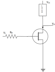
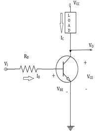
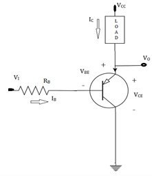
Which of the following circuits act as a switch?- a)
- b)
- c)
- d)
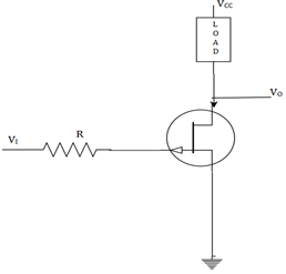
Correct answer is option 'B'. Can you explain this answer?
Which of the following circuits act as a switch?
a)
b)
c)
d)
| | Saikat Gupta answered |
This is an inverter, in which the transistor in the circuit is switched between cut off and saturation. The load, for example, can be a motor or a light emitting diode or any other electrical device.
The relation between α and β is _________- a)β=α/(1-α)
- b)α= β/(1+β)
- c)β=α/(1+α)
- d)α= β/(1- β)
Correct answer is option 'B'. Can you explain this answer?
The relation between α and β is _________
a)
β=α/(1-α)
b)
α= β/(1+β)
c)
β=α/(1+α)
d)
α= β/(1- β)
 | Kiran Gupta answered |
β is an ac base amplification factor. α is called as current amplification factor. The relation of IC and IB change as IC= βIB+ (1+ β)ICBO.
Chapter doubts & questions for Transistors - 6 Months Preparation for GATE Electrical 2026 is part of Electrical Engineering (EE) exam preparation. The chapters have been prepared according to the Electrical Engineering (EE) exam syllabus. The Chapter doubts & questions, notes, tests & MCQs are made for Electrical Engineering (EE) 2026 Exam. Find important definitions, questions, notes, meanings, examples, exercises, MCQs and online tests here.
Chapter doubts & questions of Transistors - 6 Months Preparation for GATE Electrical in English & Hindi are available as part of Electrical Engineering (EE) exam. Download more important topics, notes, lectures and mock test series for Electrical Engineering (EE) Exam by signing up for free.
6 Months Preparation for GATE Electrical675 videos|1390 docs|885 tests |