


All Exams > Electrical Engineering (EE) > 3 Months Preparation for GATE Electrical > All Questions
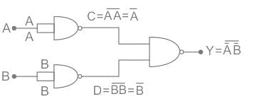
All questions of Logic Gate & Boolean Algebra for Electrical Engineering (EE) Exam
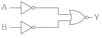
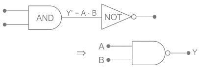
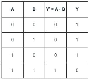
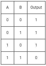
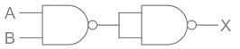
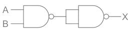
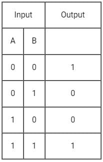
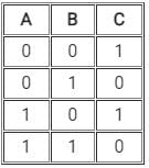
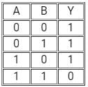
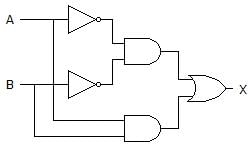
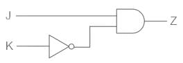
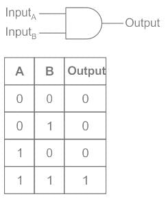
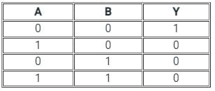
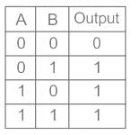
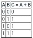
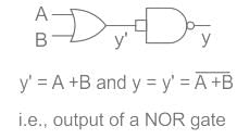
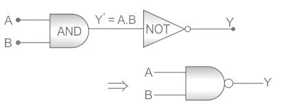
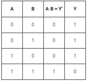
For the logic circuit shown, the truth table is :
- a)
- b)
- c)
- d)
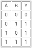
Correct answer is option 'C'. Can you explain this answer?
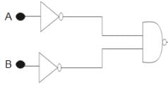
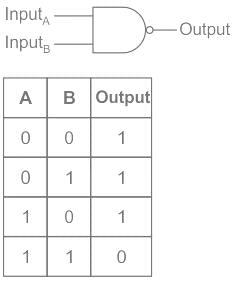
For the logic circuit shown, the truth table is :
a)
b)
c)
d)
 | Naroj Boda answered |
CONCEPT:
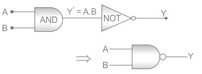
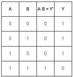
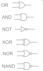
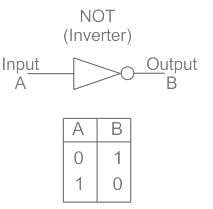
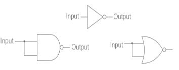
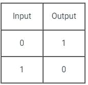
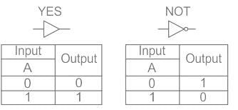
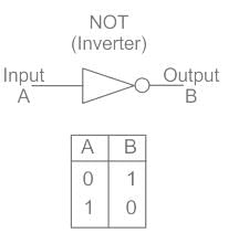
" NOT " gate - " NOT " gate is the logic gate in which input and output data are swapped. For example, if we are having input is 0 then its output is 1 and vice versa.
" NOR " gate - " NOR " gate is the type of logic gate and it is made up of the " OR " gate and the " NOT " gate.
CALCULATION:
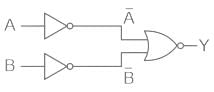
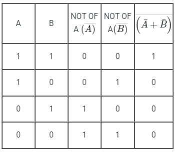
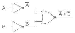
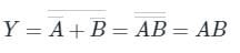
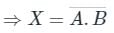
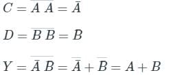
In the above figure, we have two NOT gates after the input of A and B and after that, we have a NOR gate.
" NOT " gate is represented as and " NOR " gate of
  is represented as

Using the boolean algebra rule we have;

⇒ A.B
⇒ AND Gate
Truth Table
Hence, Option 3) is the correct answer.
" NOT " gate - " NOT " gate is the logic gate in which input and output data are swapped. For example, if we are having input is 0 then its output is 1 and vice versa.
" NOR " gate - " NOR " gate is the type of logic gate and it is made up of the " OR " gate and the " NOT " gate.
CALCULATION:
In the above figure, we have two NOT gates after the input of A and B and after that, we have a NOR gate.
" NOT " gate is represented as
and " NOR " gate of is represented as Using the boolean algebra rule we have;
⇒ A.B
⇒ AND Gate
Truth Table
Hence, Option 3) is the correct answer.

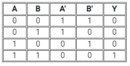
Which of the following is not true about the Logic gate?- a)It is an electronic device that implements a Boolean function
- b)It is a digital circuit that has one or more inputs but only one output
- c)There is no logical relationship between input and output voltages
- d)It follows a logical relationship between input and output voltages
Correct answer is option 'C'. Can you explain this answer?
Which of the following is not true about the Logic gate?
a)
It is an electronic device that implements a Boolean function
b)
It is a digital circuit that has one or more inputs but only one output
c)
There is no logical relationship between input and output voltages
d)
It follows a logical relationship between input and output voltages
| | Pooja Patel answered |
CONCEPT:
- Logic gate: The digital circuit that can be analyzed with the help of Boolean algebra is called a logic gate or logic circuit.
- A logic gate has two or more inputs but only one output.
- There are primarily three logic gates namely the OR gate, the AND gate, and the NOT gate.
A logic gate has one or more inputs but only one output. Thus, option 2 is correct.
It is an electronic device that implements a Boolean function. Thus option 1 is correct.
A logic gate follows a logical relationship between input and output voltages. Thus option 3 is incorrect.
It is an electronic device that implements a Boolean function. Thus option 1 is correct.
A logic gate follows a logical relationship between input and output voltages. Thus option 3 is incorrect.
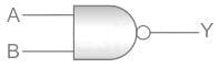
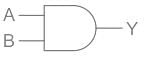
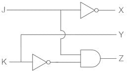
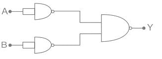
Identify the logic gate carried out by the following circuit.
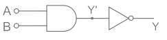
- a)OR Gate
- b)AND Gate
- c)NOR Gate
- d)NAND gate
Correct answer is option 'D'. Can you explain this answer?
Identify the logic gate carried out by the following circuit.
a)
OR Gate
b)
AND Gate
c)
NOR Gate
d)
NAND gate
| | Pooja Patel answered |
CONCEPT:
- Logic gate: The digital circuit that can be analysed with the help of Boolean algebra is called a logic gate or logic circuit.
- A logic gate has two or more inputs but only one output.
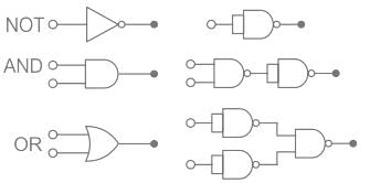
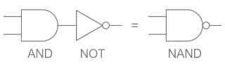
Combination of Logic Gates
The above combination of the logic gate is the NAND gate.
The above combination of the logic gate is the NAND gate.
Half adder is also known as- a)NAND
- b)AND
- c)NOT
- d)XOR
Correct answer is option 'D'. Can you explain this answer?
Half adder is also known as
a)
NAND
b)
AND
c)
NOT
d)
XOR
| | Bhavana Reddy answered |
Understanding Half Adder
A half adder is a fundamental digital circuit used in electronics to perform the arithmetic operation of addition on two binary digits. It has two inputs and two outputs.
Inputs and Outputs
- Inputs:
- A (first bit)
- B (second bit)
- Outputs:
- Sum (S)
- Carry (C)
Functionality
The half adder operates based on the following logic:
- Sum (S): The sum output is produced using the XOR (exclusive OR) operation. It gives a high output (1) when the inputs A and B are different (i.e., one is 1 and the other is 0).
- Carry (C): The carry output indicates whether there is an overflow from the addition of the two bits. It is generated using the AND operation and outputs a high signal (1) only when both inputs are 1.
Why is Half Adder Known as XOR?
- The half adder's primary function is to calculate the sum of two binary digits. The logic behind this is best represented by the XOR gate, which is defined by the following truth table:
| A | B | S (Sum) | C (Carry) |
|---|---|---------|-----------|
| 0 | 0 | 0 | 0 |
| 0 | 1 | 1 | 0 |
| 1 | 0 | 1 | 0 |
| 1 | 1 | 0 | 1 |
- The output of the Sum (S) matches the behavior of the XOR gate, confirming that the half adder is also known as an XOR circuit.
Conclusion
In summary, the half adder is essential in digital circuits for binary addition, and its sum output is directly derived from the XOR operation, making option 'D' the correct answer.
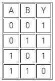
The truth table for two input logic gate is as given below
Then the logic gate is- a)NAND gate
- b)AND gate
- c)OR gate
- d)NOR gate
Correct answer is option 'A'. Can you explain this answer?
The truth table for two input logic gate is as given below
Then the logic gate is
Then the logic gate is
a)
NAND gate
b)
AND gate
c)
OR gate
d)
NOR gate
| | Pooja Patel answered |
CONCEPT:
Logic Gates:
Logic Gates:
- The logic gates are used in electronic circuits that give a certain output for a given set of Inputs.
- and which is based on a certain logic.
- Input and output are in binary form that is 1 and 0.
- It is based on certain Logic.
- Some basic logic gates are AND gate, OR gate, NOT gate.
- To build digital logic we develop a combination of these gates.
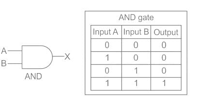
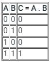
AND Gate:
- If both the inputs are high, it produces a high output.
- The Boolean algebra for AND gate is X = A. B
- It means that if any of the input of A and B is zero, the output will be zero.
- If both are one, the output will be one.
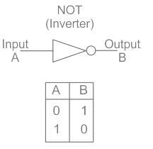
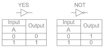
NOT gate:
- It inverts the input. Whatever the input is given, it changes its value at the output.
- The Boolean algebra for NOT gate is X = X̅
NAND Gate:
- The NAND Gate is formed by the combination of AND gate and NOT gate.
- The output obtained from AND Gate is simply reversed.
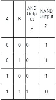
- The output of the NAND Gate is similar to the output in the question.
So, the correct option is NAND Gate.
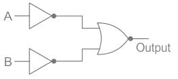
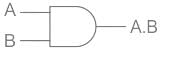
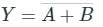
The output of the logic circuit shown in figure will be
- a)

- b)

- c)A⋅B
- d)Always zero
Correct answer is option 'C'. Can you explain this answer?
The output of the logic circuit shown in figure will be
a)
b)
c)
A⋅B
d)
Always zero
| | Pooja Patel answered |
Concept:
Logic gate: The digital circuit that can be analyzed with the help of Boolean algebra is called a logic gate or logic circuit. A logic gate has two or more inputs but only one output.
The gate given below is NAND gate
NAND gate: It a combination of an AND and a NOT gate.
From the first NAND Gate, the output will be (A⋅B)'
Now there will be 2 input of (A⋅B)' output will be [(A⋅B)']' which will give A⋅B as the correct answer.
Which one is the Universal Gate?- a)OR gate
- b)EX-OR gate
- c)NOR gate
- d)AND gate
Correct answer is option 'C'. Can you explain this answer?
Which one is the Universal Gate?
a)
OR gate
b)
EX-OR gate
c)
NOR gate
d)
AND gate
 | Cstoppers Instructors answered |
The correct answer is NOR gate.
Concept:
Concept:
- A Universal Gate is a gate by which every other gate can be realized.
- AND, OR, NOT, etc. are basic gates.
- NAND, NOR are the universal gate.
NOT, AND and OR gate realization using NAND gate is as shown:
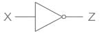
The function of a NOT logic gate is to- a)stop the input signal
- b)invert the input signal
- c)amplify the input signal
- d)none of the above
Correct answer is option 'B'. Can you explain this answer?
The function of a NOT logic gate is to
a)
stop the input signal
b)
invert the input signal
c)
amplify the input signal
d)
none of the above
| | Pooja Patel answered |
CONCEPT:
- Logic gate: Logic gates are the basic building blocks of a digital system.
- A logic gate works on the principle of a Boolean function which is a logical operation performed using one or more binary inputs that produce a single binary output.
- The boolean function uses only two variables - zero or one.
- The relationship between these inputs and the output is based on a certain logic. Based on this, logic gates are given names.
- A few logic gates along with their symbol and truth table are as follows:
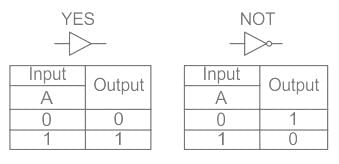
- The high and low inputs correspond to 1 and 0 respectively.
- In a NOT gate, a low output is obtained from a high input and vice versa.
- Therefore, as inferred from the truth table of the NOT gate, it inverts the input signal.
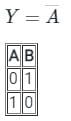
Identify the gate from the truth table
- a)NOR
- b)NAND
- c)XNOR
- d)XOR
Correct answer is option 'C'. Can you explain this answer?
Identify the gate from the truth table
a)
NOR
b)
NAND
c)
XNOR
d)
XOR
| | Pooja Patel answered |
XNOR Gate:
Symbol:
Truth Table:
Symbol:
Truth Table:
Output Equation: 
Key Points:
1) If B is always Low, the output is the inverted value of the other input A, i.e. A̅.
2) The output is low when both the inputs are different.
3) The output is high when both the inputs are the same.
4) XNOR gate produces an output only when the two inputs are the same.
Key Points:
1) If B is always Low, the output is the inverted value of the other input A, i.e. A̅.
2) The output is low when both the inputs are different.
3) The output is high when both the inputs are the same.
4) XNOR gate produces an output only when the two inputs are the same.
(A + B)(A’ * B’) = ?- a)1
- b)0
- c)AB
- d)AB’
Correct answer is option 'B'. Can you explain this answer?
(A + B)(A’ * B’) = ?
a)
1
b)
0
c)
AB
d)
AB’
| | Pooja Patel answered |
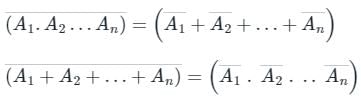
The DeMorgan’s law states that (AB)’ = A’ + B’ & (A + B)’ = A’ * B’, as per the Dual Property.
The biggest advantage of ECL is:- a)High fan-out
- b)High speed
- c)Low power consumption
- d)High density
Correct answer is option 'B'. Can you explain this answer?
The biggest advantage of ECL is:
a)
High fan-out
b)
High speed
c)
Low power consumption
d)
High density
 | Pioneer Academy answered |
ECL (Emitter Coupled Logic):
- It is fast then all logic family and very high speed in ECL transistor use in differential amplifier configuration
- When a transistor is operated in a saturation condition, due to the charge stored in the collector and base regions, it turns ON or OFF slowly. This drawback has been eliminated in ECL by operation the transistor only in the active or off region.
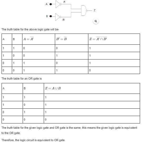
Which logic gate is equivalent to these combinations of logic gates
- a)NOR
- b)NAND
- c)AND
- d)OR
Correct answer is option 'C'. Can you explain this answer?
Which logic gate is equivalent to these combinations of logic gates
a)
NOR
b)
NAND
c)
AND
d)
OR
| | Pooja Patel answered |
CONCEPT:
Logic gates are small electronic circuits that are used to control the output current according to our requirements.
These are the following symbols to represent logic gates
These are the Properties of logic gates:
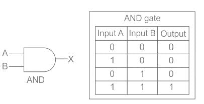
And gate(.) – It gives us an output one only when both the inputs as 1 otherwise 0
OR gate(+) – The OR gate gives an output of 1 if either of the two inputs is 1, it gives 0 otherwise.
NOT gate(‘) – The NOT gate gives an output of 1 input is 0 and vice-versa.
NOR gate – The combination of NOT and OR gates, so it will have its output reversed.
NAND gate – The combination of NOT and AND gates, so it will have its output reversed.
In our logic circuit, we used NOT and NOR in such a way that current from both A and B will pass through NOT gates and then send to the NOR gate hence the Truth table of the following circuit will be:
This means the output will be always 1 when both inputs are 1, just like the AND gate.
Logic gates are small electronic circuits that are used to control the output current according to our requirements.
These are the following symbols to represent logic gates
These are the Properties of logic gates:
And gate(.) – It gives us an output one only when both the inputs as 1 otherwise 0
OR gate(+) – The OR gate gives an output of 1 if either of the two inputs is 1, it gives 0 otherwise.
NOT gate(‘) – The NOT gate gives an output of 1 input is 0 and vice-versa.
NOR gate – The combination of NOT and OR gates, so it will have its output reversed.
NAND gate – The combination of NOT and AND gates, so it will have its output reversed.
In our logic circuit, we used NOT and NOR in such a way that current from both A and B will pass through NOT gates and then send to the NOR gate hence the Truth table of the following circuit will be:
This means the output will be always 1 when both inputs are 1, just like the AND gate.
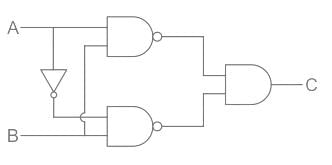
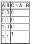
The truth table for the given logic circuit is:- a)
- b)
- c)
- d)
Correct answer is option 'D'. Can you explain this answer?
The truth table for the given logic circuit is:
a)
b)
c)
d)
| | Pooja Patel answered |
Concept:
Here we have used concept of AND, and NAND gate concepts.
If two inputs A, B are connected in And gate then the output can be written as: Y = A.B ----- (1)
In the case of the NAND gate when we connect two inputs A and b then output is: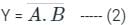
Calculation:
Given:
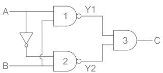
Here in this circuit, we have labeled it as 1,2,3 part of circuit having outputs Y1, Y2, and C.
Y1 = solution of first two input NAND gate, Y2 = solution of second two input NAND gate
C = solution of third AND gate connecting both NAND gates as two inputs
From the circuit diagram, we can see that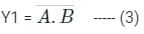
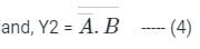
Here output C = Y2.Y1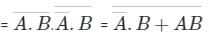 (By De Morgan's theorem)
This can be written as: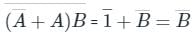
So, we can write the truth table as
when B = 0 then C = 1, B = 1 then C = 0 so that solution is completely independent on A.
So, the truth table is:
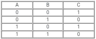
Hence option 4) is correct.
Here we have used concept of AND, and NAND gate concepts.
If two inputs A, B are connected in And gate then the output can be written as: Y = A.B ----- (1)
In the case of the NAND gate when we connect two inputs A and b then output is:
Calculation:
Given:
Here in this circuit, we have labeled it as 1,2,3 part of circuit having outputs Y1, Y2, and C.
Y1 = solution of first two input NAND gate, Y2 = solution of second two input NAND gate
C = solution of third AND gate connecting both NAND gates as two inputs
From the circuit diagram, we can see that
Here output C = Y2.Y1
(By De Morgan's theorem)This can be written as:
So, we can write the truth table as
when B = 0 then C = 1, B = 1 then C = 0 so that solution is completely independent on A.
So, the truth table is:
Hence option 4) is correct.
3 bits full adder contains ________- a)3 combinational inputs
- b)4 combinational inputs
- c)6 combinational inputs
- d)8 combinational inputs
Correct answer is option 'D'. Can you explain this answer?
3 bits full adder contains ________
a)
3 combinational inputs
b)
4 combinational inputs
c)
6 combinational inputs
d)
8 combinational inputs
| | Sushant Mukherjee answered |
A full adder is a combinational circuit that performs addition of three bits: two inputs (A and B) and a carry input (Cin). The output of a full adder consists of two bits: a sum (S) and a carry output (Cout). Therefore, a 3-bit full adder is a circuit that can perform addition of three sets of three bits.
The inputs of a 3-bit full adder are the three sets of three bits: A0, B0, Cin0, A1, B1, Cin1, A2, B2, and Cin2. Each set consists of two bits for the numbers being added (A and B) and one bit for the carry input (Cin).
To explain the answer in detail, let's break it down into headings and key points:
1. Combinational Inputs:
- A combinational input is a term used to describe an input that affects the output of a combinational circuit.
- In the case of a full adder, the combinational inputs are the three sets of three bits: A0, B0, Cin0, A1, B1, Cin1, A2, B2, and Cin2.
2. Three Sets of Three Bits:
- Each set of three bits represents the numbers being added (A and B) and the carry input (Cin) for a particular bit position.
- In a 3-bit full adder, there are three sets of three bits: A0, B0, Cin0 for the least significant bit (LSB), A1, B1, Cin1 for the middle bit, and A2, B2, Cin2 for the most significant bit (MSB).
3. Total Combinational Inputs:
- To calculate the total number of combinational inputs, we need to count the number of individual bits in all the sets.
- In a 3-bit full adder, each set consists of two bits for the numbers being added (A and B) and one bit for the carry input (Cin).
- Therefore, the total number of combinational inputs is 2 bits + 2 bits + 2 bits + 1 bit + 1 bit + 1 bit + 1 bit + 1 bit + 1 bit = 12 bits.
4. Answer Explanation:
- The correct answer is option D, which states that a 3-bit full adder contains 8 combinational inputs.
- This answer is incorrect because a 3-bit full adder consists of three sets of three bits, resulting in a total of 9 bits, not 8 bits.
- The correct answer should be option C, which states that a 3-bit full adder contains 6 combinational inputs.
In conclusion, a 3-bit full adder contains 6 combinational inputs: A0, B0, Cin0, A1, B1, and Cin1. Each set of inputs consists of two bits for the numbers being added (A and B) and one bit for the carry input (Cin).
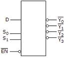
For the device shown here, assume the D input is LOW, both S inputs are LOW and the input is LOW. What is the status of the Y’ outputs?
- a)All are HIGH
- b)All are LOW
- c)All but Y0 are LOW
- d)All but Y0 are HIGH
Correct answer is option 'D'. Can you explain this answer?
For the device shown here, assume the D input is LOW, both S inputs are LOW and the input is LOW. What is the status of the Y’ outputs?
a)
All are HIGH
b)
All are LOW
c)
All but Y0 are LOW
d)
All but Y0 are HIGH
| | Pioneer Academy answered |
In the given diagram, S0 and S1 are selection bits. So,
I/P S0 S1 O/P
D = 0 0 0 Y0
D = 0 0 1 Y1
D = 0 1 0 Y2
D = 0 1 1 Y3
Hence, inputs are S0 and S1 are Low means 0, so output is Y0 and rest all are HIGH.
I/P S0 S1 O/P
D = 0 0 0 Y0
D = 0 0 1 Y1
D = 0 1 0 Y2
D = 0 1 1 Y3
Hence, inputs are S0 and S1 are Low means 0, so output is Y0 and rest all are HIGH.
What will be the output of the combination of AND gate and NOT gate if the inputs are A and B?- a)A + B
- b)A.B
- c)

- d)

Correct answer is option 'C'. Can you explain this answer?
What will be the output of the combination of AND gate and NOT gate if the inputs are A and B?
a)
A + B
b)
A.B
c)
d)
| | Pooja Patel answered |
CONCEPT
Logic gates:
Logic gates:
- It is an electric circuit, which works on simple Boolean algebra to perform a logical operation for one or more binary inputs that produce a single binary output.
Types of Logic gates:
AND Gate: If both the inputs are high, it produces a high output.
AND Gate: If both the inputs are high, it produces a high output.
- The Boolean algebra for AND gate is X = A. B
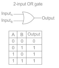
OR gate: If any of the input is high, it produces a high output.
- The Boolean algebra for OR gate is X = A + B
NOT gate: It inverts the input. Whatever the input is given, it changes its value at the output.
- The Boolean algebra for NOT gate is X = X̅
- The combination of AND gate and NOT gate gives the NAND gate.
- he Boolean algebra for AND gate is
Therefore option 3 is correct.
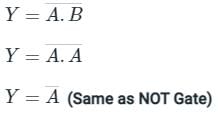
When both the input signals A and B of the NOR & NAND gate are connected together, The output of the resultant circuit will be equivalent to- a)OR
- b)AND
- c)NOT
- d)None of the above
Correct answer is option 'C'. Can you explain this answer?
When both the input signals A and B of the NOR & NAND gate are connected together, The output of the resultant circuit will be equivalent to
a)
OR
b)
AND
c)
NOT
d)
None of the above
| | Pooja Patel answered |
CONCEPT:
- Logic gate: The digital circuit that can be analyzed with the help of Boolean algebra is called a logic gate or logic circuit.
- A logic gate has two or more inputs but only one output.
- Logic gates works on the ruth table.
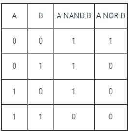
When both the input signals A and B of NOR & NAND gate are connected together, we have one common input connection hence the resultant output will be NOT gated.
As shown when both the inputs are combined in either NAND or NOR gate, they both will behave like a NOT gate
This will be the truth table for both NAND and NOR logic gate when their inputs are connected.
As shown when both the inputs are combined in either NAND or NOR gate, they both will behave like a NOT gate
This will be the truth table for both NAND and NOR logic gate when their inputs are connected.
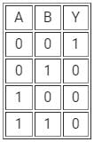
The truth table given below is for
(A and B are the inputs, Y is the output)- a)NAND
- b)XOR
- c)AND
- d)NOR
Correct answer is option 'A'. Can you explain this answer?
The truth table given below is for
(A and B are the inputs, Y is the output)
(A and B are the inputs, Y is the output)
a)
NAND
b)
XOR
c)
AND
d)
NOR
| | Pooja Patel answered |
CONCEPT:
- Truth table: A truth table is a mathematical table used to represent the output of a given function based on the combination of input variables.
- A truth table has two columns: the first column shows the combination of input variables and the last column shows the final output for each input.
- Logic gate: Logic gates are the basic building blocks of a digital system.
- A logic gate works on the principle of a Boolean function which is a logical operation performed using one or more binary inputs that produce a single binary output.
- The boolean function uses only two variables - zero or one.
- The relationship between these inputs and the output is based on a certain logic. Based on this, logic gates are given names.
- A few logic gates along with their symbol and truth table are as follows:
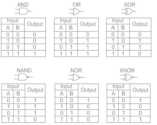
The given truth table matches with the NAND logic gate.
Any combinational circuit can be designed using only- a)AND gates
- b)OR gates
- c)XOR gates
- d)NOR gates
Correct answer is option 'D'. Can you explain this answer?
Any combinational circuit can be designed using only
a)
AND gates
b)
OR gates
c)
XOR gates
d)
NOR gates
| | Pooja Patel answered |
Concept:
A universal gate is the one with which any other Boolean function can be implemented without the need of other gates.
Two universal gates are NAND and NOR.
NAND:
In this gate, output of logic gate is false only when both the inputs are true. It is the complement of AND gate.
NOR gate: Output of this logic gate is true when both inputs are false.
Truth Table:
The involution of A is equal to _________- a)A
- b)A’
- c)1
- d)0
Correct answer is option 'A'. Can you explain this answer?
The involution of A is equal to _________
a)
A
b)
A’
c)
1
d)
0
| | Pooja Patel answered |
The involution of A means double inversion of A (i.e. A”) and is equal to A.
Proof: ((A)’)’ = A
Proof: ((A)’)’ = A
Number of 2 × 1 Multiplexers are required to implement 64 × 1 Multiplexers- a)60
- b)61
- c)62
- d)63
Correct answer is option 'D'. Can you explain this answer?
Number of 2 × 1 Multiplexers are required to implement 64 × 1 Multiplexers
a)
60
b)
61
c)
62
d)
63
| | Pooja Patel answered |
A 64 × 1 multiplexer has 64 inputs so if we use 2 × 1 multiplexers 32 are needed in the first stage for 64 inputs, the output of these 32 multiplexers are connected to inputs of 16 multiplexers in the second stage.
Similarly, in third stage, 8 (2 × 1) multiplexers are used, in fourth stage 4 are used and finally 2 (2 × 1) multiplexers in the fifth stage, 1 in the sixth stage.
Total 2 × 1 multiplexers needed are 32 + 16 + 8 + 4 + 2 + 1 = 63.
Similarly, in third stage, 8 (2 × 1) multiplexers are used, in fourth stage 4 are used and finally 2 (2 × 1) multiplexers in the fifth stage, 1 in the sixth stage.
Total 2 × 1 multiplexers needed are 32 + 16 + 8 + 4 + 2 + 1 = 63.
In the figure shown, D0 and D1 are digital inputs, S is a control input and Y is the output. When S = 0, then Y = D0. When S = 1, then Y = D1. The given combinational circuit is- a)2 input decoder
- b)2 input multiplexer
- c)Full Adder
- d)Shift Register
Correct answer is option 'B'. Can you explain this answer?
In the figure shown, D0 and D1 are digital inputs, S is a control input and Y is the output. When S = 0, then Y = D0. When S = 1, then Y = D1. The given combinational circuit is
a)
2 input decoder
b)
2 input multiplexer
c)
Full Adder
d)
Shift Register
| | Pooja Patel answered |
Multiplexers:
- A multiplexer is a combinational circuit.
- A multiplexer is Many to one data selector.
- A multiplexer selects one of the many data available at its input depending on the bits on the select line.
- For 2n inputs, there are n select lines that determine, which input is to be connected to the output.
A 2-input multiplexer is as shown below.
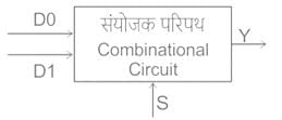
Output, Y = D0S̅ + D1S
Output, Y = D0S̅ + D1S
What determines the output from the combinational logic circuit in Digital Electronics?- a)Input signals from the past condition
- b)Input signals at the present moment
- c)Input signals from both past and present
- d)Input signals expected in future
Correct answer is option 'B'. Can you explain this answer?
What determines the output from the combinational logic circuit in Digital Electronics?
a)
Input signals from the past condition
b)
Input signals at the present moment
c)
Input signals from both past and present
d)
Input signals expected in future
| | Aniket Choudhury answered |
Explanation:
Combinational logic circuits are digital circuits that produce an output based on the current input signals. The output depends solely on the current input signals and not on any past or future input signals.
Input signals:
Input signals are the signals received by the combinational logic circuit. These signals can be either high or low, representing binary values of 1 or 0 respectively.
Present moment:
The output of the combinational logic circuit is determined by the input signals at the present moment. The circuit analyzes the current input signals and produces a corresponding output signal.
Logic gates:
Combinational logic circuits consist of logic gates such as AND gates, OR gates, and NOT gates. These gates perform logical operations on the input signals to produce the output signal.
Boolean algebra:
The behavior of the combinational logic circuit can be described using Boolean algebra. Boolean algebra is a mathematical system that deals with logical values and operations.
Conclusion:
In conclusion, the output of a combinational logic circuit is determined by the input signals at the present moment. The circuit analyzes the current input signals using logic gates and produces a corresponding output signal. The behavior of the circuit can be described using Boolean algebra.
DeMorgan’s theorem states that _________- a)(AB)’ = A’ + B’
- b)(A + B)’ = A’ * B
- c)A’ + B’ = A’B’
- d)(AB)’ = A’ + B
Correct answer is option 'A'. Can you explain this answer?
DeMorgan’s theorem states that _________
a)
(AB)’ = A’ + B’
b)
(A + B)’ = A’ * B
c)
A’ + B’ = A’B’
d)
(AB)’ = A’ + B
| | Pooja Patel answered |
The DeMorgan’s law states that (AB)’ = A’ + B’ & (A + B)’ = A’ * B’, as per the Dual Property.
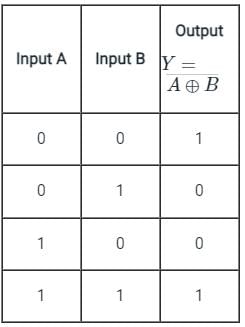
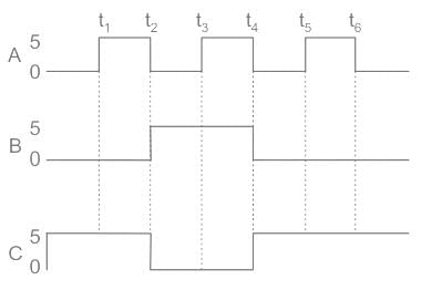
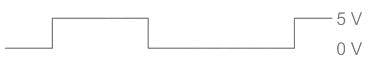
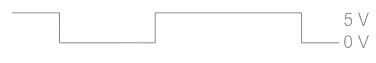
For a two-input XNOR gate, with the input waveforms as shown below, which output waveform is correct?
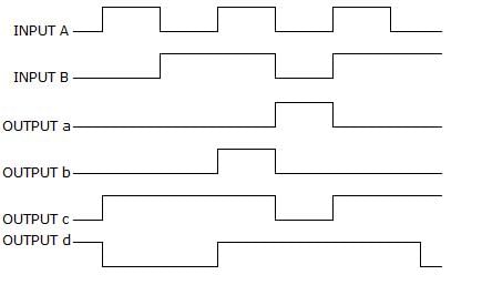
- a)d
- b)a
- c)c
- d)b
Correct answer is option 'A'. Can you explain this answer?
For a two-input XNOR gate, with the input waveforms as shown below, which output waveform is correct?
a)
d
b)
a
c)
c
d)
b
| | Pooja Patel answered |
When both inputs are same then the o/p is high for a XNOR gate.
i.e., A B O/P
0 0 1
0 1 0
1 0 0
1 1 1.
Thus, it will produce 1 when inputs are even number of 1s or all 0s, and produce 0 when input is odd number of 1s.
i.e., A B O/P
0 0 1
0 1 0
1 0 0
1 1 1.
Thus, it will produce 1 when inputs are even number of 1s or all 0s, and produce 0 when input is odd number of 1s.
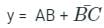
Which of the following logic expressions represents the logic diagram shown?
- a)X = AB’ + A’B
- b)X = (AB)’ + AB
- c)X = (AB)’ + A’B’
- d)X = A’B’ + AB
Correct answer is option 'D'. Can you explain this answer?
Which of the following logic expressions represents the logic diagram shown?
a)
X = AB’ + A’B
b)
X = (AB)’ + AB
c)
X = (AB)’ + A’B’
d)
X = A’B’ + AB
| | Pioneer Academy answered |
1st output of AND gate is = A’B’
2nd AND gate’s output is = AB and,
OR gate’s output is = (A’B’)+(AB) = AB + A’B’.
2nd AND gate’s output is = AB and,
OR gate’s output is = (A’B’)+(AB) = AB + A’B’.
In boolean algebra, the OR operation is performed by which properties?- a)Associative properties
- b)Commutative properties
- c)Distributive properties
- d)All of the Mentioned
Correct answer is option 'D'. Can you explain this answer?
In boolean algebra, the OR operation is performed by which properties?
a)
Associative properties
b)
Commutative properties
c)
Distributive properties
d)
All of the Mentioned
| | Cstoppers Instructors answered |
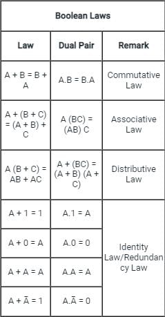
The expression for Associative property is given by A + (B + C) = (A + B) + C & A*(B*C) = (A*B)*C.
The expression for Commutative property is given by A + B = B + A & A*B = B*A.
The expression for Distributive property is given by A + BC = (A + B)(A + C) & A(B + C) = AB + AC.
The expression for Commutative property is given by A + B = B + A & A*B = B*A.
The expression for Distributive property is given by A + BC = (A + B)(A + C) & A(B + C) = AB + AC.
In a 1 to 4 De-multiplexer, how many select input lines are required?- a)2
- b)3
- c)4
- d)5
Correct answer is option 'A'. Can you explain this answer?
In a 1 to 4 De-multiplexer, how many select input lines are required?
a)
2
b)
3
c)
4
d)
5
| | Pooja Patel answered |
DEMUX:
A demultiplexer (or demux) is a device that takes a single input line and routes it to one of several digital output lines.
It consists of 2n outputs and has n selection lines, which are used to select which output line to send the input. It is also called as a data distributor.
A demultiplexer (or demux) is a device that takes a single input line and routes it to one of several digital output lines.
It consists of 2n outputs and has n selection lines, which are used to select which output line to send the input. It is also called as a data distributor.
A combinational logic circuit for traffic control is designed. ___________ GATE can only be used to implement the designed control circuit without any additional GATES.- a)NOT
- b)EXOR
- c)AND
- d)NAND
Correct answer is option 'D'. Can you explain this answer?
A combinational logic circuit for traffic control is designed. ___________ GATE can only be used to implement the designed control circuit without any additional GATES.
a)
NOT
b)
EXOR
c)
AND
d)
NAND
| | Pooja Patel answered |
The logic gate for traffic control is:
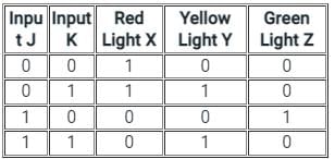
For red light
Output X = NOT (J)
For yellow light
Output Y = K

For green light:
Output Z = J AND (NOT K)
Combined Circuit is given as,
Now, all the gates can be formed from NAND gate, as it is a universal gate.
NAND gate will be the correct answer.
For red light
Output X = NOT (J)
For yellow light
Output Y = K
For green light:
Output Z = J AND (NOT K)
Combined Circuit is given as,
Now, all the gates can be formed from NAND gate, as it is a universal gate.
NAND gate will be the correct answer.
_______ are an example of a combinational circuit.- a)Shift Registers
- b)Multiplexers
- c)Counters
- d)Flip-Flops
Correct answer is option 'B'. Can you explain this answer?
_______ are an example of a combinational circuit.
a)
Shift Registers
b)
Multiplexers
c)
Counters
d)
Flip-Flops
| | Pooja Patel answered |
Combinational Logic circuits:
Combinational Logic circuits are circuits for which the present output depends only on the present input, i.e. there is no memory element to store the past output.
A combinational circuit can have ‘n’ number of inputs and ‘m’ number of outputs as shown:
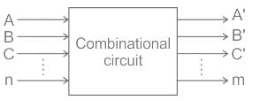
Combinational circuits are:
Combinational Logic circuits are circuits for which the present output depends only on the present input, i.e. there is no memory element to store the past output.
A combinational circuit can have ‘n’ number of inputs and ‘m’ number of outputs as shown:
Combinational circuits are:
- Multiplexer/Demultiplexer
- Encoder/Decoder
- Adders
- Subtractors
- Code Converters
Multiplexers:
- A multiplexer is Many to one data selector.
- A multiplexer selects one of the many data available at its input depending on the bits on the select line.
- For 2m inputs, there are m select lines that determine which input is to be connected to the output.
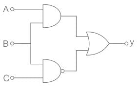
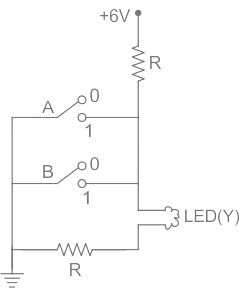
For the given circuit, the input digital signals are applied at the terminals A, B and C. What would be the output at the terminal y ?
- a)
- b)
- c)

- d)
Correct answer is option 'C'. Can you explain this answer?
For the given circuit, the input digital signals are applied at the terminals A, B and C. What would be the output at the terminal y ?
a)
b)
c)
d)
| | Pioneer Academy answered |
Concept:
Logic gates are:
1.AND Gate
2. NAND Gate
3. OR Gate
Calculation:
Output of combination of logic gates is given as
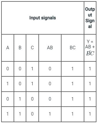
So the output y is high i.e., 1.
Hence, Output voltage is V0 = 5 V.
Logic gates are:
1.AND Gate
2. NAND Gate
3. OR Gate
Calculation:
Output of combination of logic gates is given as
So the output y is high i.e., 1.
Hence, Output voltage is V0 = 5 V.
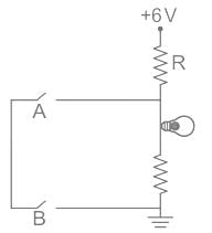
If the glow of the bulb is considered an output, the correct Boolean operation represented by the circuit diagram drawn will be:- a)AND
- b)OR
- c)NAND
- d)NOR
Correct answer is option 'C'. Can you explain this answer?
If the glow of the bulb is considered an output, the correct Boolean operation represented by the circuit diagram drawn will be:
a)
AND
b)
OR
c)
NAND
d)
NOR
| | Pooja Patel answered |
From the given circuit we can see that,
- Two Keys are connected parallel to a LED and a resistor.
- Hence if any of the keys is open, no current will flow through keys and hence bulb will glow
- But if both the keys are closed current will start flowing from keys instead of LEDs, since current (I) will always flow where resistance is minimum.
- Which means the truth table for the given circuit can be given as
- Here 1 shows key is closed and current can flows through it
- And 0 shows key is open and current can’t flow through it
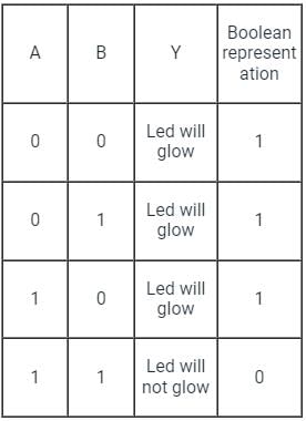
The circuit diagram shown here corresponds to the logic gate
- a)OR
- b)NAND
- c)NOR
- d)AND
Correct answer is option 'C'. Can you explain this answer?
The circuit diagram shown here corresponds to the logic gate
a)
OR
b)
NAND
c)
NOR
d)
AND
| | Naroj Boda answered |
CONCEPT:
- OR gate - The OR gate is defined as the gate in which if one of the inputs is true then the result will also true.
- AND gate - The AND gate is defined as the gate in which if one of the inputs is false then the result will also false.
- NOT gate - The NOT gate is defined as the output attains state 1 if and only if the input does not attain state 1.
- NOR gate - NOR gate is defined as it is the combination of NOT and OR gate.
CALCULATION:
Let us the different cases.
Case I - When A = 0, B = 0
The LED will glow.
Therefore, Y = 1
Case II - When A = 1, B = 0
The LED will not glow.
Therefore, Y = 0
Case III - When A = 0, B = 1
The LED will not glow.
Therefore, Y = 0
Case IV - When A = 1, B = 1
The LED will glow.
Therefore, Y = 0
The truth table is written as;
Here we see the results it will show the nature of NOR.
Hence, option 3) is the correct answer.
If A = 1 and B = 0, then in terms of Boolean algebra, A + B̅ =- a)B
- b)B̅
- c)A
- d)A̅
Correct answer is option 'C'. Can you explain this answer?
If A = 1 and B = 0, then in terms of Boolean algebra, A + B̅ =
a)
B
b)
B̅
c)
A
d)
A̅
| | Partho Saha answered |
Explanation:
Boolean Algebra Basics:
- In Boolean algebra, the variables can have only two possible values: 0 or 1.
- The basic operations in Boolean algebra are AND, OR, and NOT, denoted by symbols: &, +, and ' respectively.
A + B in Boolean Algebra:
- In Boolean algebra, the operation '+' represents the OR operation.
- A + B means A OR B, which is true if at least one of the variables A or B is true.
- Given A = 1 and B = 0, A + B will be true because A is true (1) even though B is false (0).
Substitute A and B:
- Substituting the given values, A = 1 and B = 0, into the expression A + B:
- 1 + 0 = 1 (since OR operation is true if at least one variable is true).
Final Answer:
- Therefore, in terms of Boolean algebra, A + B = A.
- Hence, the correct answer is option 'C', which is A.
The expression for Absorption law is given by _________- a)A + AB = A
- b)A + AB = B
- c)AB + AA’ = A
- d)A + B = B + A
Correct answer is option 'A'. Can you explain this answer?
The expression for Absorption law is given by _________
a)
A + AB = A
b)
A + AB = B
c)
AB + AA’ = A
d)
A + B = B + A
| | Cstoppers Instructors answered |
The expression for Absorption Law is given by: A+AB = A.
Proof: A + AB = A(1 + B) = A (Since 1 + B = 1 as per 1’s Property).
Proof: A + AB = A(1 + B) = A (Since 1 + B = 1 as per 1’s Property).
Choose the incorrect statement regarding logic gates.- a)Logic gates works on truth table
- b)Logic gates are used to switch on or off for any instrument
- c)Logic gates are used as fuse in electric circuit
- d)All are incorrect
Correct answer is option 'C'. Can you explain this answer?
Choose the incorrect statement regarding logic gates.
a)
Logic gates works on truth table
b)
Logic gates are used to switch on or off for any instrument
c)
Logic gates are used as fuse in electric circuit
d)
All are incorrect
| | Luminary Institute answered |
CONCEPT:
- Logic gate: The digital circuit that can be analyzed with the help of Boolean algebra is called a logic gate or logic circuit.
- A logic gate has two or more inputs but only one output.
- Logic gates work on the truth table.
AND Gate: The Logic AND Gate is a type of digital logic circuit whose output goes 1 (HIGH) only when all of its inputs are 1 (HIGH)
The truth table for AND gate:
- As the logic gates give only one output. It is not the continuous output giving element. But the fuse should work continuously. That's why the logic gates can’t be used as a fuse in an electric circuit. So statement 3 is wrong. So option 3 is correct.
- As the logic gates give only one output. It is not the continuous output giving element. In case of an on or off alarms, we just need only one output, either on or off. That's why the logic gates can be used to on or off the alarm. So statement 2 is correct.
- The logic gates work on the truth table as shown in the example on the concept part because it can give either yes or no as output. So statement 1 is correct.
Identify the logic gate
- a)OR gate
- b)AND gate
- c)NOT gate
- d)NOR gate
Correct answer is option 'A'. Can you explain this answer?
Identify the logic gate
a)
OR gate
b)
AND gate
c)
NOT gate
d)
NOR gate
| | Luminary Institute answered |
CONCEPT:
- Logic gate: The digital circuit that can be analysed with the help of Boolean algebra is called a logic gate or logic circuit.
- A logic gate has two or more inputs but only one output.
OR gate: It is a digital circuit having two or more inputs but only one output.
It gives a high output if either input A or B or both are high (1) otherwise it gives a low output (0).
It is described by the Boolean expression: A + B = Y
The above logic gate is the OR gate.
The truth table of OR gate:
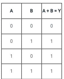
It gives a high output if either input A or B or both are high (1) otherwise it gives a low output (0).
It is described by the Boolean expression: A + B = Y
The above logic gate is the OR gate.
The truth table of OR gate:
The carry propagation can be expressed as ________- a)Cp = AB
- b)Cp = A + B
- c)All but Y0 are LOW
- d)All but Y0 are HIGH
Correct answer is option 'B'. Can you explain this answer?
The carry propagation can be expressed as ________
a)
Cp = AB
b)
Cp = A + B
c)
All but Y0 are LOW
d)
All but Y0 are HIGH
| | Aarya Basu answered |
Carry Propagation in Digital Logic
Explanation:
The carry propagation is a concept in digital logic that refers to the process of carrying over a bit from one stage to the next in a multi-bit binary addition or subtraction operation. It ensures that the correct result is obtained when adding or subtracting numbers with multiple bits.
Carry Propagation Equation:
The carry propagation can be expressed as:
Cp = A & B
where Cp is the carry output, A is the input from the previous stage, and B is the input from the current stage.
Explanation of the Carry Propagation Equation:
In a multi-bit binary addition or subtraction operation, each stage consists of two inputs (A and B) and one output (Cp). The input A is the carry input from the previous stage, and the input B is the bit being added/subtracted at the current stage.
The carry propagation equation Cp = A & B represents the logic operation performed to determine the carry output. The "&" symbol represents the logical AND operation.
Logic behind the Carry Propagation Equation:
The carry output (Cp) will be HIGH (1) if and only if both the carry input (A) and the bit being added/subtracted (B) are HIGH (1). In all other cases, the carry output will be LOW (0).
Answer Justification:
Option B, Cp = A & B, is the correct answer because it accurately represents the carry propagation equation. The carry output is determined by performing a logical AND operation between the carry input and the bit being added/subtracted.
Options A, C, and D are incorrect:
- Option A, Cp = AB, is not a valid representation of the carry propagation equation. It suggests a logical AND operation between A and B, without considering the carry input from the previous stage.
- Option C, All but Y0 are LOW, does not provide any information about the carry propagation equation. It seems unrelated to the given question.
- Option D, All but Y0 are HIGH, also does not provide any information about the carry propagation equation. It seems unrelated to the given question.
Hence, the correct answer is option B, Cp = A & B.
Simplify Y = AB’ + (A’ + B)C.- a)AB’ + C
- b)AB + AC
- c)A’B + AC’
- d)AB + A
Correct answer is option 'A'. Can you explain this answer?
Simplify Y = AB’ + (A’ + B)C.
a)
AB’ + C
b)
AB + AC
c)
A’B + AC’
d)
AB + A
| | Pooja Patel answered |
Y = AB’ + (A’ + B)C = AB’ + (AB’)’C = (AB’ + C)( AB’ + AB’) = (AB’ + C).1 = (AB’ + C).
What is the indication of a short to ground in the output of a driving gate?- a)Only the output of the defective gate is affected
- b)There is a signal loss to all load gates
- c)The node may be stuck in either the HIGH or the LOW state
- d)The affected node will be stuck in the HIGH state
Correct answer is option 'B'. Can you explain this answer?
What is the indication of a short to ground in the output of a driving gate?
a)
Only the output of the defective gate is affected
b)
There is a signal loss to all load gates
c)
The node may be stuck in either the HIGH or the LOW state
d)
The affected node will be stuck in the HIGH state
| | Sparsh Nambiar answered |
Indication of a short to ground in the output of a driving gate
When there is a short to ground in the output of a driving gate, it means that there is a direct connection between the output node of the gate and the ground. This can occur due to a fault or malfunction in the gate or its surrounding circuitry. The indication of this short can be observed through certain effects and behaviors exhibited by the gate and its output.
Effects of a short to ground
- Signal loss to all load gates: One of the main indications of a short to ground in the output of a driving gate is that there will be a signal loss to all the load gates connected to the output. The short effectively grounds the output node, preventing any signal from being transmitted to the load gates. As a result, these load gates will not receive the intended signals, leading to a loss of functionality or incorrect operation.
Other possible effects
- Node stuck in either the HIGH or LOW state: In some cases, a short to ground in the output of a driving gate can cause the affected node to become stuck in either the HIGH or LOW state. This is because the short effectively creates a direct path to ground, bypassing the normal operation of the gate. Depending on the specific circuit configuration and the nature of the short, the affected node may remain either HIGH or LOW regardless of the input signals.
It is important to note that the specific effects and behaviors observed may vary depending on the gate technology, circuit configuration, and the nature of the short itself. Therefore, it is necessary to carefully analyze the circuit and perform troubleshooting to accurately identify and address the issue.
In conclusion, when there is a short to ground in the output of a driving gate, the main indication is a signal loss to all load gates connected to the output. Additionally, the affected node may become stuck in either the HIGH or LOW state, depending on the circuit configuration.
Which logic gate will produce the following output?
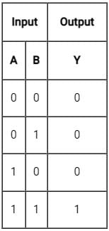
- a)OR
- b)AND
- c)NAND
- d)NOR
Correct answer is option 'B'. Can you explain this answer?
Which logic gate will produce the following output?
a)
OR
b)
AND
c)
NAND
d)
NOR
| | Pooja Patel answered |
CONCEPT
Logic gates:
Logic gates:
- It is an electric circuit, which works on simple Boolean algebra to perform a logical operation for one or more binary inputs that produce a single binary output.
Types of Logic gates:
AND Gate: If both the inputs are high, it produces a high output.
AND Gate: If both the inputs are high, it produces a high output.
- The Boolean algebra for AND gate is X = A. B
And NAND gate is opposite of AND gate which means output is one when any of input is 1 whereas if both inputs is 1 output is 0
OR gate: If any of the input is high, it produces a high output.
OR gate: If any of the input is high, it produces a high output.
- The Boolean algebra for OR gate is X = A + B
NOT gate: It inverts the input. Whatever the input is given, it changes its value at the output.
- The Boolean algebra for NOT gate is X = X̅
From the above explanation, we can see that in our case the output for a given truth table is only possible for AND gate.
The basic gates are:- a)AND, NOR and NOT gate
- b)AND, OR and NOT gate
- c)AND and NOT gate
- d)OR and NOT gate
Correct answer is option 'B'. Can you explain this answer?
The basic gates are:
a)
AND, NOR and NOT gate
b)
AND, OR and NOT gate
c)
AND and NOT gate
d)
OR and NOT gate
| | Pooja Patel answered |
- AND, OR, NOT gates are the basic gates.
- The logic gates which are derived from the basic gates like AND, OR, NOT gates are known as derived gates. NAND, NOR, XOR, and XNOR are the derived gates.
- A universal gate is a gate which can implement any Boolean function without need to use any other gate type. The NAND and NOR gates are universal gates.
The output of an OR gate is connected to both the inputs of a NAND gate. The combination will serve as- a)AND gate
- b)NOT gate
- c)NAND gate
- d)NOR gate
Correct answer is option 'D'. Can you explain this answer?
The output of an OR gate is connected to both the inputs of a NAND gate. The combination will serve as
a)
AND gate
b)
NOT gate
c)
NAND gate
d)
NOR gate
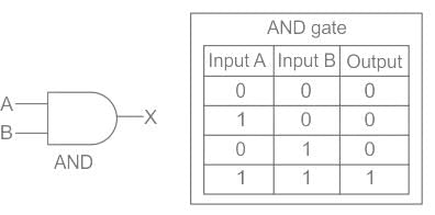
| | Pooja Patel answered |
CONCEPT:
- AND Gate: The Logic AND Gate is a digital logic circuit whose output is 1 (HIGH) only when all the inputs are 1 (HIGH)
- OR Gate: The Logic OR Gate is a digital logic circuit whose output goes HIGH to a logic level 1 only when one or more of its inputs are HIGH

- NOT Gate: The Logic NOT Gate is the most basic of all the logic gates and is often referred to as an Inverting Buffer or simply an Inverter.
- NAND Gate: The logic Gate is obtained after adding NOT Gate after AND Gate.

- NOR Gate: The logic Gate is obtained after adding NOT Gate after OR Gate.
- Since the output of OR Gate is input for both the inputs of NAND Gates, Both the inputs will be the same.
- When a NAND gate is connected to the same input it acts as a NOT Gate.
- The output of NAND Gate will be (same input)
- If NOT Gate is added after OR Gate, It will act as NOR Gate.
- So, The output of an OR gate is connected to both the inputs of a NAND gate. The combination will serve as NOR Gate. Hence the correct answer is option 4.
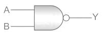
Identify the logic gate?
- a)OR gate
- b)AND gate
- c)NOT gate
- d)NAND gate
Correct answer is option 'D'. Can you explain this answer?
Identify the logic gate?
a)
OR gate
b)
AND gate
c)
NOT gate
d)
NAND gate
| | Pooja Patel answered |
CONCEPT:
- Logic gate: The digital circuit that can be analyzed with the help of Boolean algebra is called a logic gate or logic circuit.
- A logic gate has two or more inputs but only one output.
NAND gate: It a combination of an AND and a NOT gate.
It is obtained by connecting the output fo an AND gate to the input of a NOT gate.
It is described by the Boolean expression:
The above logic gate is the NAND gate.
The truth table of NAND gate:
It is described by the Boolean expression:
The above logic gate is the NAND gate.
The truth table of NAND gate:
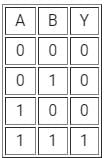
The truth table given below corresponds to-
- a)NOR gate
- b)NAND gate
- c)AND gate
- d)XOR gate
Correct answer is option 'A'. Can you explain this answer?
The truth table given below corresponds to-
a)
NOR gate
b)
NAND gate
c)
AND gate
d)
XOR gate
| | Cstoppers Instructors answered |
CONCEPT:
- Truth table: A truth table is a mathematical table used to represent the output of a given function based on the combination of input variables.
- A truth table has two columns: the first column shows the combination of input variables and the last column shows the final output for each input.
- Logic gate: Logic gates are the basic building blocks of a digital system.
- A logic gate works on the principle of a Boolean function which is a logical operation performed using one or more binary inputs that produce a single binary output.
- The boolean function uses only two variables - zero or one.
- The relationship between these inputs and the output is based on a certain logic. Based on this, logic gates are given names.
- A few logic gates along with their symbol and truth table are as follows:
The given truth table matches with the NOR logic gate.
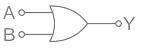
Identify the logic operation carried out by the following circuit.
- a)AND
- b)NAND
- c)NOR
- d)OR
Correct answer is option 'D'. Can you explain this answer?
Identify the logic operation carried out by the following circuit.
a)
AND
b)
NAND
c)
NOR
d)
OR
| | Pioneer Academy answered |
Concept:
De Morgan’s law states that:
This is OR gate. So option 4 is correct.
De Morgan’s law states that:
This is OR gate. So option 4 is correct.
Which of the following combinations of logic gates can decode binary 1101?- a)One 4-input AND gate
- b)One 4-input AND gate, one inverter
- c)One 4-input AND gate, one OR gate
- d)One 4-input NAND gate, one inverter
Correct answer is option 'B'. Can you explain this answer?
Which of the following combinations of logic gates can decode binary 1101?
a)
One 4-input AND gate
b)
One 4-input AND gate, one inverter
c)
One 4-input AND gate, one OR gate
d)
One 4-input NAND gate, one inverter
| | Pooja Patel answered |
For decoding any number output must be high for that code and this is possible in One 4-input NAND gate, one inverter option only. A decoder is a combinational circuit that converts binary data to n-coded data upto 2n outputs.
Complement of the expression A’B + CD’ is _________- a)(A’ + B)(C’ + D)
- b)(A + B’)(C’ + D)
- c)(A + B’)(C + D’)
- d)None of these
Correct answer is option 'B'. Can you explain this answer?
Complement of the expression A’B + CD’ is _________
a)
(A’ + B)(C’ + D)
b)
(A + B’)(C’ + D)
c)
(A + B’)(C + D’)
d)
None of these
| | Pooja Patel answered |
(A’B + CD’)’ = (A’B)'(CD’)’ (By DeMorgan’s Theorem) = (A” + B’)(C’ + D”) (By DeMorgan’s Theorem) = (A + B’)(C’ + D).
Chapter doubts & questions for Logic Gate & Boolean Algebra - 3 Months Preparation for GATE Electrical 2026 is part of Electrical Engineering (EE) exam preparation. The chapters have been prepared according to the Electrical Engineering (EE) exam syllabus. The Chapter doubts & questions, notes, tests & MCQs are made for Electrical Engineering (EE) 2026 Exam. Find important definitions, questions, notes, meanings, examples, exercises, MCQs and online tests here.
Chapter doubts & questions of Logic Gate & Boolean Algebra - 3 Months Preparation for GATE Electrical in English & Hindi are available as part of Electrical Engineering (EE) exam. Download more important topics, notes, lectures and mock test series for Electrical Engineering (EE) Exam by signing up for free.
3 Months Preparation for GATE Electrical676 videos|1399 docs|882 tests |