


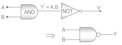
All Exams > Electrical Engineering (EE) > 3 Months Preparation for GATE Electrical > All Questions
All questions of Basics of Digital Electronics for Electrical Engineering (EE) Exam
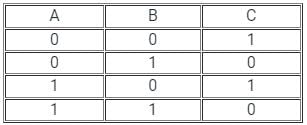
Each product term of a group, w’.x.y’ and w.y, represents the ____________ in that group.- a)Input
- b)POS
- c)Sum-of-Minterms
- d)Sum of Maxterms
Correct answer is option 'C'. Can you explain this answer?
Each product term of a group, w’.x.y’ and w.y, represents the ____________ in that group.
a)
Input
b)
POS
c)
Sum-of-Minterms
d)
Sum of Maxterms
 | Husban Yousaf answered |
Because minters are called products of logic and of sets of variables

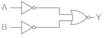
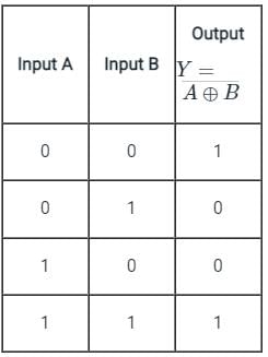
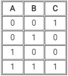
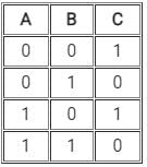
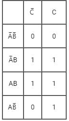
For the logic circuit shown, the truth table is :
- a)
- b)
- c)
- d)
Correct answer is option 'C'. Can you explain this answer?
For the logic circuit shown, the truth table is :
a)
b)
c)
d)
 | Naroj Boda answered |
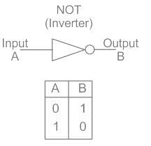
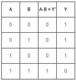
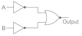
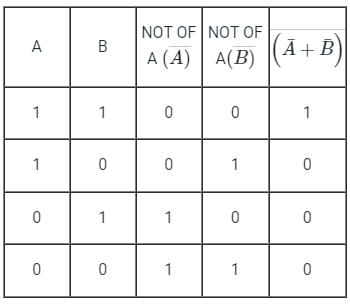
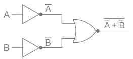
CONCEPT:
" NOT " gate - " NOT " gate is the logic gate in which input and output data are swapped. For example, if we are having input is 0 then its output is 1 and vice versa.
" NOR " gate - " NOR " gate is the type of logic gate and it is made up of the " OR " gate and the " NOT " gate.
CALCULATION:
In the above figure, we have two NOT gates after the input of A and B and after that, we have a NOR gate.
" NOT " gate is represented as and " NOR " gate of
  is represented as

Using the boolean algebra rule we have;

⇒ A.B
⇒ AND Gate
Truth Table
Hence, Option 3) is the correct answer.
" NOT " gate - " NOT " gate is the logic gate in which input and output data are swapped. For example, if we are having input is 0 then its output is 1 and vice versa.
" NOR " gate - " NOR " gate is the type of logic gate and it is made up of the " OR " gate and the " NOT " gate.
CALCULATION:
In the above figure, we have two NOT gates after the input of A and B and after that, we have a NOR gate.
" NOT " gate is represented as
and " NOR " gate of is represented as Using the boolean algebra rule we have;
⇒ A.B
⇒ AND Gate
Truth Table
Hence, Option 3) is the correct answer.
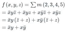
Simplify the Boolean expression:
F(w,x,y,z) = ∑ (0,1,2,4,5,6,8,9,12,13,14)- a)w+x+y+z
- b)y’ + w’z’+xz’
- c)y + w’z’+xz
- d)x+z’w’y+x’
Correct answer is option 'B'. Can you explain this answer?
Simplify the Boolean expression:
F(w,x,y,z) = ∑ (0,1,2,4,5,6,8,9,12,13,14)
F(w,x,y,z) = ∑ (0,1,2,4,5,6,8,9,12,13,14)
a)
w+x+y+z
b)
y’ + w’z’+xz’
c)
y + w’z’+xz
d)
x+z’w’y+x’
| | Vaishnavi Singh answered |
F(w,x,y,z) = wxy + w'xy'z + w'x'y + w'x'yz + wx'y'z + w'xyz + w'xy'z + w'x'yz
Simplified expression: F(w,x,y,z) = wxy + w'x'y + wx'y'z + w'xyz + w'x'yz
Simplified expression: F(w,x,y,z) = wxy + w'x'y + wx'y'z + w'xyz + w'x'yz
Half adder is also known as- a)NAND
- b)AND
- c)NOT
- d)XOR
Correct answer is option 'D'. Can you explain this answer?
Half adder is also known as
a)
NAND
b)
AND
c)
NOT
d)
XOR
| | Bhavana Reddy answered |
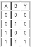
Understanding Half Adder
A half adder is a fundamental digital circuit used in electronics to perform the arithmetic operation of addition on two binary digits. It has two inputs and two outputs.
Inputs and Outputs
- Inputs:
- A (first bit)
- B (second bit)
- Outputs:
- Sum (S)
- Carry (C)
Functionality
The half adder operates based on the following logic:
- Sum (S): The sum output is produced using the XOR (exclusive OR) operation. It gives a high output (1) when the inputs A and B are different (i.e., one is 1 and the other is 0).
- Carry (C): The carry output indicates whether there is an overflow from the addition of the two bits. It is generated using the AND operation and outputs a high signal (1) only when both inputs are 1.
Why is Half Adder Known as XOR?
- The half adder's primary function is to calculate the sum of two binary digits. The logic behind this is best represented by the XOR gate, which is defined by the following truth table:
| A | B | S (Sum) | C (Carry) |
|---|---|---------|-----------|
| 0 | 0 | 0 | 0 |
| 0 | 1 | 1 | 0 |
| 1 | 0 | 1 | 0 |
| 1 | 1 | 0 | 1 |
- The output of the Sum (S) matches the behavior of the XOR gate, confirming that the half adder is also known as an XOR circuit.
Conclusion
In summary, the half adder is essential in digital circuits for binary addition, and its sum output is directly derived from the XOR operation, making option 'D' the correct answer.
Binary coded decimal is a combination of __________- a)Two binary digits
- b)Three binary digits
- c)Four binary digits
- d)Five binary digits
Correct answer is option 'C'. Can you explain this answer?
Binary coded decimal is a combination of __________
a)
Two binary digits
b)
Three binary digits
c)
Four binary digits
d)
Five binary digits
 | Mihir Kulkarni answered |
Introduction
Binary coded decimal (BCD) is a numerical representation system that uses a combination of binary digits to represent decimal numbers. Each decimal digit is represented by a 4-bit binary code, allowing for easy conversion between binary and decimal representations.
Explanation
BCD uses four binary digits to represent each decimal digit. This allows for a direct one-to-one mapping between decimal and binary representations, making it easier to perform arithmetic operations on decimal numbers using binary logic.
Binary Digits
In binary representation, each digit can have two possible values: 0 or 1. Therefore, a single binary digit can represent two different values. However, a decimal digit can have ten possible values: 0 to 9. To represent all ten decimal digits using binary digits, we need to use a combination of multiple binary digits.
Decimal Digits
In the decimal number system, we have ten digits: 0, 1, 2, 3, 4, 5, 6, 7, 8, and 9. These digits can be represented using four binary digits, as shown below:
- Decimal digit 0 is represented as 0000 in BCD.
- Decimal digit 1 is represented as 0001 in BCD.
- Decimal digit 2 is represented as 0010 in BCD.
- Decimal digit 3 is represented as 0011 in BCD.
- Decimal digit 4 is represented as 0100 in BCD.
- Decimal digit 5 is represented as 0101 in BCD.
- Decimal digit 6 is represented as 0110 in BCD.
- Decimal digit 7 is represented as 0111 in BCD.
- Decimal digit 8 is represented as 1000 in BCD.
- Decimal digit 9 is represented as 1001 in BCD.
Example
Let's take an example to understand how BCD works. Suppose we want to represent the decimal number 25 in BCD.
- The decimal digit 2 is represented as 0010 in BCD.
- The decimal digit 5 is represented as 0101 in BCD.
Therefore, the BCD representation of the decimal number 25 is 0010 0101.
Conclusion
In conclusion, BCD is a numerical representation system that uses four binary digits to represent each decimal digit. This allows for a direct mapping between decimal and binary representations, making it easier to perform arithmetic operations on decimal numbers using binary logic.
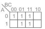
Which of the following is the Boolean function for Majority Voting, assuming A, B, C are inputs and Y is output?- a)Y = AB + AC + CB
- b)Y = A + B + C
- c)Y = ABC
- d)Y = AB + BC
Correct answer is option 'A'. Can you explain this answer?
Which of the following is the Boolean function for Majority Voting, assuming A, B, C are inputs and Y is output?
a)
Y = AB + AC + CB
b)
Y = A + B + C
c)
Y = ABC
d)
Y = AB + BC
| | Pooja Patel answered |
Concept:
Majority voting means when more than 1 inputs one 1 (i.e. when 2 or more inputs are 1).
Majority voting means when more than 1 inputs one 1 (i.e. when 2 or more inputs are 1).
Calculation:
Truth Table is as shown:
Solving using K-map we get,
Q = AC + BC + AB
Truth Table is as shown:
Solving using K-map we get,
Q = AC + BC + AB
The 2’s complement of 1010101 is ______.- a)0101010
- b)1110011
- c)0101011
- d)1101010
Correct answer is option 'C'. Can you explain this answer?
The 2’s complement of 1010101 is ______.
a)
0101010
b)
1110011
c)
0101011
d)
1101010
| | Sarthak Yadav answered |
Understanding 2's Complement
The 2's complement is a method used to represent negative numbers in binary. To find the 2's complement of a binary number, follow these steps:
1. **Invert the Bits**: Change all 0s to 1s and all 1s to 0s.
2. **Add One**: Add 1 to the inverted binary number.
Steps to Find the 2's Complement of 1010101
1. **Original Binary Number**:
- 1010101
2. **Invert the Bits**:
- 0 → 1
- 1 → 0
- Therefore, the inverted bits become:
- 0101010
3. **Add One**:
- Adding 1 to the inverted number:
- 0101010
- + 1
- __________
- 0101011
Final Result
Thus, the 2's complement of 1010101 is 0101011.
Conclusion
The correct answer is option 'C' (0101011). This method is crucial in digital systems for arithmetic operations and representing negative numbers effectively. Understanding the 2's complement is essential for anyone studying Electrical Engineering and working with binary systems.
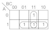
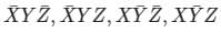
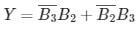
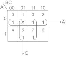
Consider the following sum of products expression, F

The equivalent product of sums expression is- a)
- b)
- c)
- d)
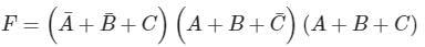
Correct answer is option 'A'. Can you explain this answer?
Consider the following sum of products expression, F
The equivalent product of sums expression is
The equivalent product of sums expression is
a)
b)
c)
d)
| | Pooja Patel answered |
Concept:
The SOP representation of the circuit is:
F = Σm (minterms)
Minterm: a minterm of n variables is a product of the variables in which each appears exactly once in true or complemented form.
The POS representation of the circuit:
F = ΠM (max terms)
Maxterm: a maxterm of n variables is a sum of the variables in which each appears exactly once in true or complemented form.
Calculation:
Given,

For the function, we form the K-map as:
Hence, the function in the form of minterms is expressed as:
f(A, B, C) = Σm (0,1,3,5,7)
Now, we put 0 in each block of the K-map excluding the blocks corresponding to the terms in the above function.
Grouping the 0’s in K-map, we obtain the max terms as
F = πM(2, 4, 6)

Given,
For the function, we form the K-map as:
Hence, the function in the form of minterms is expressed as:
f(A, B, C) = Σm (0,1,3,5,7)
Now, we put 0 in each block of the K-map excluding the blocks corresponding to the terms in the above function.
Grouping the 0’s in K-map, we obtain the max terms as
F = πM(2, 4, 6)
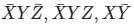
In the sum of products function (X, Y, Z) = ∑(2, 3, 4, 5), the prime implicants are- a)

- b)
- c)
- d)
Correct answer is option 'A'. Can you explain this answer?
In the sum of products function (X, Y, Z) = ∑(2, 3, 4, 5), the prime implicants are
a)
b)
c)
d)
 | Cstoppers Instructors answered |
So, there are only two implicants,

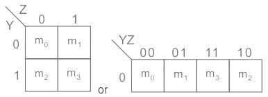
A K-map of 3 variables contains _______ cells.- a)8
- b)3
- c)6
- d)9
Correct answer is option 'A'. Can you explain this answer?
A K-map of 3 variables contains _______ cells.
a)
8
b)
3
c)
6
d)
9
| | Pooja Patel answered |
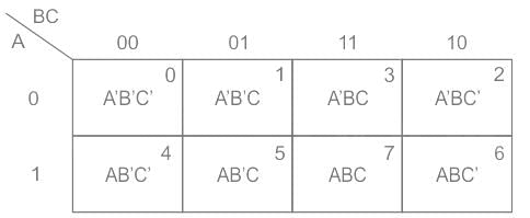
Karnaugh map (K-map):
- The Karnaugh map (K-map) is a method of simplifying Boolean algebra expressions.
- The Karnaugh map reduces the need for extensive calculations.
- Karnaugh map can be explained as An array that contains 2k number of cells, where k is the number of variables in the Boolean expression that is to be reduced or optimized.
Number of cells in 2 variable k-map = 22 = 4
Number of cells in 3 variable k-map = 23 = 8
Number of cells in 4 variable k-map = 24 = 16
Number of cells in 3 variable k-map = 23 = 8
Number of cells in 4 variable k-map = 24 = 16
2 variable K-maps:
There are 4 cells in the 2-variable k-map as shown,
There are 4 cells in the 2-variable k-map as shown,
3 variable K-maps:
- For a 3-variable Boolean function, there is a possibility of 8 output minterms.
- The general representation of all the minterms using 3-variables is shown below.
Looping on a K-map always results in the elimination of __________- a)Variables within the loop that appear only in their complemented form
- b)Variables that remain unchanged within the loop
- c)Variables within the loop that appear in both complemented and uncomplemented form
- d)Variables within the loop that appear only in their uncomplemented form
Correct answer is option 'C'. Can you explain this answer?
Looping on a K-map always results in the elimination of __________
a)
Variables within the loop that appear only in their complemented form
b)
Variables that remain unchanged within the loop
c)
Variables within the loop that appear in both complemented and uncomplemented form
d)
Variables within the loop that appear only in their uncomplemented form
| | Snehal Rane answered |
Explanation:
Looping on a K-map refers to the process of identifying groups of adjacent 1s or 0s in a Karnaugh map to simplify a Boolean expression. When performing this process, it is important to note the following:
Variables within the loop that appear in both complemented and uncomplemented form:
When looping on a K-map, the primary objective is to identify adjacent 1s or 0s to form a group or loop. The variables within this loop can appear in both complemented (denoted by an overline) and uncomplemented (denoted without an overline) form. This means that the variable can appear as both a 1 and a 0 within the loop, depending on the combination of inputs. These variables are essential for forming the loop and cannot be eliminated.
Variables within the loop that appear only in their uncomplemented form:
In the process of looping on a K-map, it is possible to have variables that appear only in their uncomplemented form within the loop. These variables are necessary for forming the loop and cannot be eliminated.
Variables within the loop that appear only in their complemented form:
Variables within the loop that appear only in their complemented form can be eliminated. These variables do not affect the formation of the loop and can be removed from the Boolean expression.
Conclusion:
Looping on a K-map always results in the elimination of variables within the loop that appear in both complemented and uncomplemented form. These variables are necessary for forming the loop and cannot be eliminated. Variables that appear only in their complemented form can be eliminated, while variables that appear only in their uncomplemented form are necessary for forming the loop and cannot be eliminated. Therefore, the correct answer is option 'C'.
Which statement below best describes a Karnaugh map?- a)It is simply a rearranged truth table
- b)The Karnaugh map eliminates the need for using NAND and NOR gates
- c)Variable complements can be eliminated by using Karnaugh maps
- d)A Karnaugh map can be used to replace Boolean rules
Correct answer is option 'A'. Can you explain this answer?
Which statement below best describes a Karnaugh map?
a)
It is simply a rearranged truth table
b)
The Karnaugh map eliminates the need for using NAND and NOR gates
c)
Variable complements can be eliminated by using Karnaugh maps
d)
A Karnaugh map can be used to replace Boolean rules
| | Isha Singh answered |
Introduction:
A Karnaugh map, also known as a K-map, is a graphical representation of a truth table. It is a useful tool in digital logic design for simplifying Boolean functions and minimizing the number of gates required to implement a logic circuit.
Explanation:
1. A rearranged truth table:
A Karnaugh map is a rearranged version of a truth table that provides a visual representation of the Boolean function. In a truth table, the outputs are listed in a tabular format, whereas in a Karnaugh map, the inputs and outputs are represented by squares or cells in a grid-like structure. Each cell corresponds to a particular combination of input values.
2. Eliminates the need for using NAND and NOR gates:
The Karnaugh map itself does not eliminate the need for using NAND and NOR gates. It is a tool that helps in simplifying Boolean functions, which in turn can reduce the number of gates required for implementation. By using a Karnaugh map, one can identify patterns and group adjacent cells with the same output value, which leads to simplified Boolean expressions and potentially reduces the number of gates needed.
3. Variable complements can be eliminated by using Karnaugh maps:
Variable complements, or negations, are not eliminated by using Karnaugh maps. In fact, Karnaugh maps can help identify and exploit complementarity relationships to simplify Boolean expressions. By grouping cells that differ by only one variable, complement terms can be canceled out, resulting in a simplified expression.
4. A Karnaugh map can be used to replace Boolean rules:
A Karnaugh map is not used to replace Boolean rules but rather as a tool to simplify Boolean functions. Boolean rules, such as De Morgan's theorem or the distributive property, are fundamental principles that govern Boolean algebra. Karnaugh maps, on the other hand, provide a visual representation that aids in simplification.
Conclusion:
In conclusion, the statement "It is simply a rearranged truth table" best describes a Karnaugh map. While a Karnaugh map does not eliminate the need for using NAND and NOR gates, it helps in simplifying Boolean functions and reducing the number of gates required for implementation. Moreover, Karnaugh maps do not eliminate variable complements but can exploit complementarity relationships to simplify Boolean expressions. Finally, Karnaugh maps are not used to replace Boolean rules but rather as a tool to aid in simplification.
The binary code of (21.125)10 is- a)10101.001
- b)10100.001
- c)10101.010
- d)10100.111
Correct answer is option 'A'. Can you explain this answer?
The binary code of (21.125)10 is
a)
10101.001
b)
10100.001
c)
10101.010
d)
10100.111
| | Janhavi Roy answered |
Binary Code of (21.125)10
To convert a decimal number to binary, we need to divide the decimal number by 2 repeatedly until the quotient becomes zero. The binary representation is obtained by writing the remainders in reverse order. In this case, we need to convert the decimal number 21.125 to binary.
Step 1: Integer Part Conversion
To convert the integer part of the decimal number (21), we divide it by 2 repeatedly until the quotient becomes zero.
21 ÷ 2 = 10 with a remainder of 1
10 ÷ 2 = 5 with a remainder of 0
5 ÷ 2 = 2 with a remainder of 1
2 ÷ 2 = 1 with a remainder of 0
1 ÷ 2 = 0 with a remainder of 1
The remainders in reverse order are 10101, which is the binary representation of the integer part of the decimal number.
Step 2: Fractional Part Conversion
To convert the fractional part of the decimal number (0.125), we multiply it by 2 repeatedly until it becomes zero or until the desired number of binary places are obtained.
0.125 × 2 = 0.25 (0)
0.25 × 2 = 0.5 (0)
0.5 × 2 = 1.0 (1)
The binary representation of the fractional part is 001. Therefore, the binary representation of the decimal number 21.125 is 10101.001.
Answer: Option A - 10101.001
Don’t care conditions can be used for simplifying Boolean expressions in ___________- a)Registers
- b)Terms
- c)K-maps
- d)Latches
Correct answer is option 'C'. Can you explain this answer?
Don’t care conditions can be used for simplifying Boolean expressions in ___________
a)
Registers
b)
Terms
c)
K-maps
d)
Latches
| | Mansi Choudhury answered |
I'm sorry, I don't understand what you are asking. Can you please provide more context or clarify your question?
The decimal number 10 is represented in its BCD form as __________- a)10100000
- b)01010111
- c)00010000
- d)00101011
Correct answer is option 'C'. Can you explain this answer?
The decimal number 10 is represented in its BCD form as __________
a)
10100000
b)
01010111
c)
00010000
d)
00101011
| | Pooja Patel answered |
The decimal number 10 is represented in its BCD form as 0001 0000, in accordance to 8421 for each of the two digits.
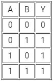
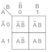
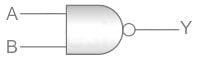
The truth table for two input logic gate is as given below
Then the logic gate is- a)NAND gate
- b)AND gate
- c)OR gate
- d)NOR gate
Correct answer is option 'A'. Can you explain this answer?
The truth table for two input logic gate is as given below
Then the logic gate is
Then the logic gate is
a)
NAND gate
b)
AND gate
c)
OR gate
d)
NOR gate
| | Pooja Patel answered |
CONCEPT:
Logic Gates:
Logic Gates:
- The logic gates are used in electronic circuits that give a certain output for a given set of Inputs.
- and which is based on a certain logic.
- Input and output are in binary form that is 1 and 0.
- It is based on certain Logic.
- Some basic logic gates are AND gate, OR gate, NOT gate.
- To build digital logic we develop a combination of these gates.
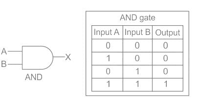
AND Gate:
- If both the inputs are high, it produces a high output.
- The Boolean algebra for AND gate is X = A. B
- It means that if any of the input of A and B is zero, the output will be zero.
- If both are one, the output will be one.
NOT gate:
- It inverts the input. Whatever the input is given, it changes its value at the output.
- The Boolean algebra for NOT gate is X = X̅
NAND Gate:
- The NAND Gate is formed by the combination of AND gate and NOT gate.
- The output obtained from AND Gate is simply reversed.
- The output of the NAND Gate is similar to the output in the question.
So, the correct option is NAND Gate.
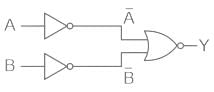
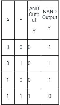
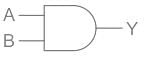
The output of the logic circuit shown in figure will be
- a)

- b)

- c)A⋅B
- d)Always zero
Correct answer is option 'C'. Can you explain this answer?
The output of the logic circuit shown in figure will be
a)
b)
c)
A⋅B
d)
Always zero
| | Naroj Boda answered |
Concept:
Logic gate: The digital circuit that can be analyzed with the help of Boolean algebra is called a logic gate or logic circuit. A logic gate has two or more inputs but only one output.
The gate given below is NAND gate
NAND gate: It a combination of an AND and a NOT gate.
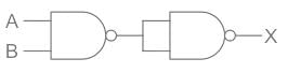
From the first NAND Gate, the output will be (A⋅B)'
Now there will be 2 input of (A⋅B)' output will be [(A⋅B)']' which will give A⋅B as the correct answer.
Logic gate: The digital circuit that can be analyzed with the help of Boolean algebra is called a logic gate or logic circuit. A logic gate has two or more inputs but only one output.
The gate given below is NAND gate
NAND gate: It a combination of an AND and a NOT gate.
From the first NAND Gate, the output will be (A⋅B)'
Now there will be 2 input of (A⋅B)' output will be [(A⋅B)']' which will give A⋅B as the correct answer.
The simplification in minimal sum of product (SOP) of Y = F(A, B, C, D) = ∑m (0, 2, 3, 6, 7) + ∑d (8, 10, 11, 15) using K-maps is- a)Y = AC + BD̅
- b)Y = AC̅ + BD̅
- c)Y = A̅ C̅ + B̅ D
- d)Y = A̅ C + B̅ D̅
Correct answer is option 'D'. Can you explain this answer?
The simplification in minimal sum of product (SOP) of Y = F(A, B, C, D) = ∑m (0, 2, 3, 6, 7) + ∑d (8, 10, 11, 15) using K-maps is
a)
Y = AC + BD̅
b)
Y = AC̅ + BD̅
c)
Y = A̅ C̅ + B̅ D
d)
Y = A̅ C + B̅ D̅
| | Pallabi Pillai answered |
Y = F(A, B, C, D) = A'BC'D' + AB'C'D' + AB'CD' + ABCD' + ABC'D + A'BCD + A'B'CD + A'B'C'D
A boolean function is given as F(x, y, z) = ∑(1, 3, 6, 7). What is its equivalent canonical form?- a)F(x, y, z) = ∏ (0, 2, 3, 5) product of max terms
- b)F(x, y, z) = ∏ (0, 2, 4, 5) product of max terms
- c)F(x, y, z) = ∏ (0, 2, 4, 5) product of min terms
- d)F(x, y, z) = ∏ (0, 2, 4, 5) sum of max terms
Correct answer is option 'B'. Can you explain this answer?
A boolean function is given as F(x, y, z) = ∑(1, 3, 6, 7). What is its equivalent canonical form?
a)
F(x, y, z) = ∏ (0, 2, 3, 5) product of max terms
b)
F(x, y, z) = ∏ (0, 2, 4, 5) product of max terms
c)
F(x, y, z) = ∏ (0, 2, 4, 5) product of min terms
d)
F(x, y, z) = ∏ (0, 2, 4, 5) sum of max terms
| | Rajesh Kumar answered |
The question seems to be incomplete. Please provide the complete boolean function F(x, y, z) and I will be happy to help you with it.
Identify the gate from the truth table
- a)NOR
- b)NAND
- c)XNOR
- d)XOR
Correct answer is option 'C'. Can you explain this answer?
Identify the gate from the truth table
a)
NOR
b)
NAND
c)
XNOR
d)
XOR
 | Pioneer Academy answered |
XNOR Gate:
Symbol:
Truth Table:
Symbol:
Truth Table:
Output Equation: 
Key Points:
1) If B is always Low, the output is the inverted value of the other input A, i.e. A̅.
2) The output is low when both the inputs are different.
3) The output is high when both the inputs are the same.
4) XNOR gate produces an output only when the two inputs are the same.
Key Points:
1) If B is always Low, the output is the inverted value of the other input A, i.e. A̅.
2) The output is low when both the inputs are different.
3) The output is high when both the inputs are the same.
4) XNOR gate produces an output only when the two inputs are the same.
(A + B)(A’ * B’) = ?- a)1
- b)0
- c)AB
- d)AB’
Correct answer is option 'B'. Can you explain this answer?
(A + B)(A’ * B’) = ?
a)
1
b)
0
c)
AB
d)
AB’
| | Pooja Patel answered |
The DeMorgan’s law states that (AB)’ = A’ + B’ & (A + B)’ = A’ * B’, as per the Dual Property.
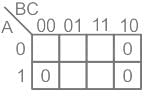
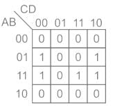
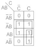
The output expression for the Karnaugh map shown below is:
- a)BD̅ + BCD
- b)BD̅ + AB
- c)B̅D + ABC
- d)BD̅ + ABC
Correct answer is option 'D'. Can you explain this answer?
The output expression for the Karnaugh map shown below is:
a)
BD̅ + BCD
b)
BD̅ + AB
c)
B̅D + ABC
d)
BD̅ + ABC
| | Pioneer Academy answered |
Given K-map:
It can be grouped as follows:
Output expression in the form of SOP (sum of products) = BD̅ + ABC
It can be grouped as follows:
Output expression in the form of SOP (sum of products) = BD̅ + ABC
The biggest advantage of ECL is:- a)High fan-out
- b)High speed
- c)Low power consumption
- d)High density
Correct answer is option 'B'. Can you explain this answer?
The biggest advantage of ECL is:
a)
High fan-out
b)
High speed
c)
Low power consumption
d)
High density
| | Pioneer Academy answered |
ECL (Emitter Coupled Logic):
- It is fast then all logic family and very high speed in ECL transistor use in differential amplifier configuration
- When a transistor is operated in a saturation condition, due to the charge stored in the collector and base regions, it turns ON or OFF slowly. This drawback has been eliminated in ECL by operation the transistor only in the active or off region.
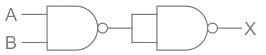
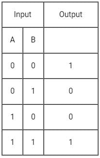
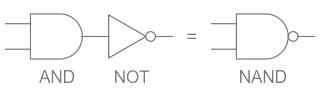
Which logic gate is equivalent to these combinations of logic gates
- a)NOR
- b)NAND
- c)AND
- d)OR
Correct answer is option 'C'. Can you explain this answer?
Which logic gate is equivalent to these combinations of logic gates
a)
NOR
b)
NAND
c)
AND
d)
OR
| | Pooja Patel answered |
CONCEPT:
Logic gates are small electronic circuits that are used to control the output current according to our requirements.
These are the following symbols to represent logic gates
These are the Properties of logic gates:
And gate(.) – It gives us an output one only when both the inputs as 1 otherwise 0
OR gate(+) – The OR gate gives an output of 1 if either of the two inputs is 1, it gives 0 otherwise.
NOT gate(‘) – The NOT gate gives an output of 1 input is 0 and vice-versa.
NOR gate – The combination of NOT and OR gates, so it will have its output reversed.
NAND gate – The combination of NOT and AND gates, so it will have its output reversed.
In our logic circuit, we used NOT and NOR in such a way that current from both A and B will pass through NOT gates and then send to the NOR gate hence the Truth table of the following circuit will be:
This means the output will be always 1 when both inputs are 1, just like the AND gate.
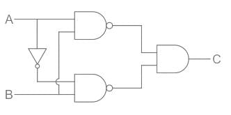
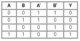
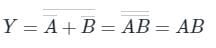
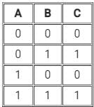
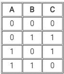
The truth table for the given logic circuit is:- a)
- b)
- c)
- d)
Correct answer is option 'D'. Can you explain this answer?
The truth table for the given logic circuit is:
a)
b)
c)
d)
| | Pooja Patel answered |
Concept:
Here we have used concept of AND, and NAND gate concepts.
If two inputs A, B are connected in And gate then the output can be written as: Y = A.B ----- (1)
In the case of the NAND gate when we connect two inputs A and b then output is: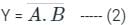
Calculation:
Given:
Here in this circuit, we have labeled it as 1,2,3 part of circuit having outputs Y1, Y2, and C.
Y1 = solution of first two input NAND gate, Y2 = solution of second two input NAND gate
C = solution of third AND gate connecting both NAND gates as two inputs
From the circuit diagram, we can see that
Here output C = Y2.Y1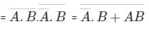 (By De Morgan's theorem)
This can be written as: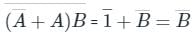
So, we can write the truth table as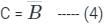
when B = 0 then C = 1, B = 1 then C = 0 so that solution is completely independent on A.
So, the truth table is:
Hence option 4) is correct.
Here we have used concept of AND, and NAND gate concepts.
If two inputs A, B are connected in And gate then the output can be written as: Y = A.B ----- (1)
In the case of the NAND gate when we connect two inputs A and b then output is:
Calculation:
Given:
Here in this circuit, we have labeled it as 1,2,3 part of circuit having outputs Y1, Y2, and C.
Y1 = solution of first two input NAND gate, Y2 = solution of second two input NAND gate
C = solution of third AND gate connecting both NAND gates as two inputs
From the circuit diagram, we can see that
Here output C = Y2.Y1
(By De Morgan's theorem)This can be written as:
So, we can write the truth table as
when B = 0 then C = 1, B = 1 then C = 0 so that solution is completely independent on A.
So, the truth table is:
Hence option 4) is correct.
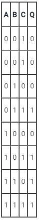
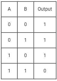
A problem detector system produces an alarm in the factory when one of the three conditions occurs. The system is designed as such tha only one condition can occur at a time. If the three conditions are defined as q, r, and s respectively, the output logic for the system is given as- a)q̅rs + r̅ s̅
- b)qr̅ s̅ + q̅sr̅ + q̅rs̅
- c)qrs̅ + r̅
- d)q + r + s
Correct answer is option 'B'. Can you explain this answer?
A problem detector system produces an alarm in the factory when one of the three conditions occurs. The system is designed as such tha only one condition can occur at a time. If the three conditions are defined as q, r, and s respectively, the output logic for the system is given as
a)
q̅rs + r̅ s̅
b)
qr̅ s̅ + q̅sr̅ + q̅rs̅
c)
qrs̅ + r̅
d)
q + r + s
| | Pooja Patel answered |
Concept:
K maps
This is a table that represents both minterms and max terms in it and it is used for the simplification of the boolean algebraic expressions easily.
For an 'n' variable k-map total 2n cells will be present in it.
The different k-maps structures are shown below:
2 variable k-map
3 variable k-map
Calculation:
- Given conditions for the system are
- A problem detector system produces an alarm in the factory when one of the three conditions occurs.
- The system is designed as such only one condition can occur at a time.
- conditions are defined as q, r, and s
The truth table is shown as:
The output function minterms according to the truth table are:
output = ∑ (1, 2, 4)
k-map for the circuit is:
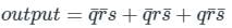
The output function minterms according to the truth table are:
output = ∑ (1, 2, 4)
k-map for the circuit is:
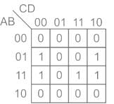
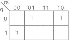
Write the simplified equation for the given K-Map.
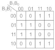
- a)
- b)
- c)
- d)
Correct answer is option 'A'. Can you explain this answer?
Write the simplified equation for the given K-Map.
a)
b)
c)
d)
| | Pioneer Academy answered |
Concept:
K-map:
K-map:
- K-map (Karnaugh Map) is a pictorial method used to minimize Boolean expression without having to use Boolean Algebra theorems and equation manipulation.
- K-map can be thought of as a special version of a truth table.
- Using K-map, expression with two to four variables are easily minimized.
- K-maps are also referred to as 2D truth tables as each K-map is nothing but a different format of representing the values present in a one-dimensional truth table.
- To simplify a logic expression with two inputs, we require a K-map with 4 cells (= 22)
- Similarly, a logic expression with four inputs we require a K-map with 16 cells (= 24)
- Each cell within K-map has a definite place value which is obtained by using on encoding technique known as Gray code.
- For n-variable K-map, with 2n cells, try to group 2n cells first, then for 2n-1 cells, next for 2n-2 cells, and so on until the group contains only 2° cells ie. Isolated bits (if any)
- Also remember, the number of cells in a group must be equal to an integer power to 2 i.e. 1, 2, 4, 8, ….
Calculation:
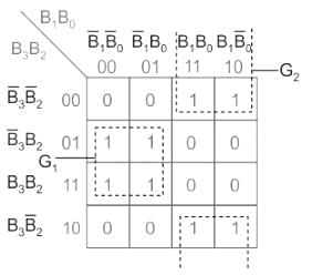
→ There are no 16 bits group, no 8-bits group, but there are 2-four bits group
→ Eliminate the variables for which the corresponding hit appears within the group as both 0 and 1.
→ Eliminate the variables for which the corresponding hit appears within the group as both 0 and 1.
- Group 1 → B̅1 B2
- Group 2 → B1 B̅2
→ Therefore in SOP form (sum of products) output 
A three digit decimal number requires ________ for representation in the conventional BCD format.- a)3 bits
- b)6 bits
- c)12 bits
- d)24 bits
Correct answer is option 'C'. Can you explain this answer?
A three digit decimal number requires ________ for representation in the conventional BCD format.
a)
3 bits
b)
6 bits
c)
12 bits
d)
24 bits
| | Prasenjit Yadav answered |
A three-digit decimal number can range from 100 to 999. In the conventional BCD (Binary Coded Decimal) format, each decimal digit is represented by a 4-bit binary code.
Let's break down the representation of a three-digit decimal number in the BCD format:
- The first digit can have values from 1 to 9. In the BCD format, it requires 4 bits to represent each value. So, for the first digit, we need 4 bits.
- The second and third digits can have values from 0 to 9. Again, each digit requires 4 bits to represent each value. So, for the second and third digits, we need 4 bits each.
To find the total number of bits required for the representation of a three-digit decimal number, we add up the bits required for each digit.
- Bits required for the first digit: 4 bits
- Bits required for the second digit: 4 bits
- Bits required for the third digit: 4 bits
Adding them up, we get a total of 4 + 4 + 4 = 12 bits.
Therefore, a three-digit decimal number requires 12 bits for representation in the conventional BCD format.
Convert the 127 decimal number into binary.- a)1100111
- b)1111111
- c)1111011
- d)111111
Correct answer is option 'B'. Can you explain this answer?
Convert the 127 decimal number into binary.
a)
1100111
b)
1111111
c)
1111011
d)
111111
| | Ashwin Kapoor answered |
Understanding the Conversion of Decimal to Binary
To convert a decimal number into binary, we need to understand the binary number system, which is base 2, using only the digits 0 and 1. Each binary digit represents a power of 2, starting from the rightmost digit (which represents 2^0).
Step-by-Step Conversion of 127 to Binary
1. Identify the Largest Power of 2
The largest power of 2 less than or equal to 127 is 2^6, which is 64.
2. Subtract and Find Remaining Value
- 127 - 64 = 63
- The next largest power of 2 less than or equal to 63 is 2^5 (32).
- 63 - 32 = 31
- Next, 2^4 (16) gives 31 - 16 = 15.
- Next, 2^3 (8) gives 15 - 8 = 7.
- Next, 2^2 (4) gives 7 - 4 = 3.
- Next, 2^1 (2) gives 3 - 2 = 1.
- Finally, 2^0 (1) gives 1 - 1 = 0.
3. Write the Binary Representation
Since we used powers of 2 from 2^0 to 2^6, we can represent 127 in binary as:
- 2^6 (1), 2^5 (1), 2^4 (1), 2^3 (1), 2^2 (1), 2^1 (1), 2^0 (1) → 1111111
Final Answer Evaluation
Among the options provided:
- a) 1100111: This is 103 in decimal.
- b) 1111111: This is 127 in decimal (Correct Answer).
- c) 1111011: This is 123 in decimal.
- d) 111111: This is 63 in decimal.
Thus, option 'b' (1111111) is the accurate binary representation of the decimal number 127.
Conversion of (98.75)10 into binary, octal and hexadecimal number system, respectively, is:- a)(1100010.11)2 (246.6)8 and (62.C)16
- b)(0100011.11)2 (142.6)8 and (62.C)16
- c)(0100011.11)2 (242.6)8 and (62.12)16
- d)(1100010.11)2 (142.6)8 and (62.C)16
Correct answer is option 'D'. Can you explain this answer?
Conversion of (98.75)10 into binary, octal and hexadecimal number system, respectively, is:
a)
(1100010.11)2 (246.6)8 and (62.C)16
b)
(0100011.11)2 (142.6)8 and (62.C)16
c)
(0100011.11)2 (242.6)8 and (62.12)16
d)
(1100010.11)2 (142.6)8 and (62.C)16
| | Pooja Patel answered |
Concept:
Conversion of decimal to binary:
Step 1: Divide the number by 2 keeping notice of the quotient and the remainder. Continue dividing the quotient by 2 until you get a quotient of zero.
Step 2: Write out the remainders in the reverse order to get the equivalent binary number.
Step 1: Divide the number by 2 keeping notice of the quotient and the remainder. Continue dividing the quotient by 2 until you get a quotient of zero.
Step 2: Write out the remainders in the reverse order to get the equivalent binary number.
For converting decimal fractions to binary numbers, follow these steps:
For converting decimal fractions to a binary numbers, follow these steps:
Then write out the integer parts from the results of each multiplication to get the equivalent binary number.
For converting decimal fractions to a binary numbers, follow these steps:
Then write out the integer parts from the results of each multiplication to get the equivalent binary number.
Conversion of binary to octal:
Make pair of three binary number which forms an octal number.
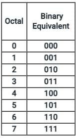
Make pair of three binary number which forms an octal number.
Conversion of binary to hexadecimal:
Make pair of four binary number which forms a hexadecimal number.
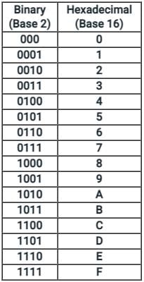
Make pair of four binary number which forms a hexadecimal number.
Calculation:
Given, that the decimal number = (98.75)10
98 / 2 = 49 with remainder 0
49 / 2 = 24 with remainder 1
24 / 2 = 12 with remainder 0
12 / 2 = 6 with remainder 0
6 / 2 = 3 with remainder 0
3 / 2 = 1 with remainder 1
1 / 2 = 0 with remainder 1
Write in reverse order:
98 = 1100010
0.75 × 2 = 1 + 0.5
0.5 × 2 = 1 + 0
.75 = .11
(98.75)10 = (1100010.11)2
(98.75)10 = (001 100 010. 110)2 = (142.6)8 ...........(from table 1)
(98.75)10 = (0110 0010. 1100)2 = (62.C)16...........(from table 2)
The excess-3 code for 597 is given by __________- a)100011001010
- b)100010100111
- c)010110010111
- d)010110101101
Correct answer is option 'A'. Can you explain this answer?
The excess-3 code for 597 is given by __________
a)
100011001010
b)
100010100111
c)
010110010111
d)
010110101101
| | Pooja Patel answered |
The addition of ‘3’ to each digit yields the three new digits ‘8’, ’12’ and ’10’. Hence, the corresponding four-bit binary equivalents are 100011001010, in accordance to 8421 format.
The systematic reduction of logic circuits is accomplished by _______________- a)Symbolic reduction
- b)TTL logic
- c)Using Boolean algebra
- d)Using a truth table
Correct answer is option 'C'. Can you explain this answer?
The systematic reduction of logic circuits is accomplished by _______________
a)
Symbolic reduction
b)
TTL logic
c)
Using Boolean algebra
d)
Using a truth table
| | Pooja Patel answered |
The systematic reduction of logic circuits is accomplished by using boolean algebra.
Digital input signals A, B, C with A as the MSB and C as the LSB are used to realize the Boolean function F = m0 + m2 + m3 + m5 + m7, where mi denotes the ith minterm. In addition, F has a don’t care for m1. The simplified expression for F is given by:- a)
- b)

- c)

- d)
Correct answer is option 'B'. Can you explain this answer?
Digital input signals A, B, C with A as the MSB and C as the LSB are used to realize the Boolean function F = m0 + m2 + m3 + m5 + m7, where mi denotes the ith minterm. In addition, F has a don’t care for m1. The simplified expression for F is given by:
a)
b)
c)
d)
| | Pooja Patel answered |
F = m0 + m2 + m3 + m5 + m7
m1 is a don’t care.
m1 is a don’t care.
Which of the following statements accurately represents the two BEST methods of logic circuit simplification?- a)Actual circuit trial and error evaluation and waveform analysis
- b)Karnaugh mapping and circuit waveform analysis
- c)Boolean algebra and Karnaugh mapping
- d)Boolean algebra and actual circuit trial and error evaluation
Correct answer is option 'C'. Can you explain this answer?
Which of the following statements accurately represents the two BEST methods of logic circuit simplification?
a)
Actual circuit trial and error evaluation and waveform analysis
b)
Karnaugh mapping and circuit waveform analysis
c)
Boolean algebra and Karnaugh mapping
d)
Boolean algebra and actual circuit trial and error evaluation
| | Pooja Patel answered |
The two BEST methods of logic circuit simplification are Boolean algebra and Karnaugh mapping. Boolean Algebra uses the Laws of Boolean Algebra for minimization of Boolean expressions while Karnaugh Map is a pictorial representation and reduction of the Boolean expression.
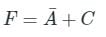
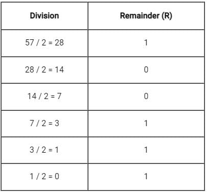
The decimal number (57.375)10 when converted to binary number takes the form:- a)(111001.011)2
- b)(100111.110)2
- c)(110011.101)2
- d)(111011.011)2
Correct answer is option 'A'. Can you explain this answer?
The decimal number (57.375)10 when converted to binary number takes the form:
a)
(111001.011)2
b)
(100111.110)2
c)
(110011.101)2
d)
(111011.011)2
| | Pooja Patel answered |
Concept:
Decimal to binary:
- Take decimal number as dividend.
- Divide the number by 2.
- Get the integer quotient for the next iteration.
- Get the remainder (it will be either 0 or 1 because of divisor 2).
- Repeat the steps until the quotient is equal to 0
- Write the remainders in reverse order (which will be equivalent binary number of given decimal number).
Decimal to binary: (fractional part)
- Take decimal number as multiplicand.
- Multiple this number by 2 (2 is base of binary so multiplier here).
- Store the value of integer part of result in an array (it will be either 0 or 1 because of multiplier 2).
- Repeat the above two steps until the number became zero.
- Write these resultant integer part
Calculation:
Binary of 57:
Now, write remainder from bottom to up (in reverse order), this will be 111001 which is equivalent binary number of decimal integer 57.
Convert decimal fractional number 0.375 into binary number.
Here, decimal fraction: 0.375
Now, write these resultant integer part, this will be 0.0110 which is equivalent binary fractional number of decimal fractional 0.375.
∴ 57.375 can be written as 111001.011 in binary
Hence, option (1) is correct.
Which of the following statement is NOT correct?- a)Hexadecimal number uses sixteen distinct counting digits 0 through 9 and A through F
- b)The 1’s complement of a binary number is obtained by changing its each 0 into a 1
- c)Octal number has a base of 7
- d)Excess-3 Code is an unweighted code
Correct answer is option 'C'. Can you explain this answer?
Which of the following statement is NOT correct?
a)
Hexadecimal number uses sixteen distinct counting digits 0 through 9 and A through F
b)
The 1’s complement of a binary number is obtained by changing its each 0 into a 1
c)
Octal number has a base of 7
d)
Excess-3 Code is an unweighted code
| | Pooja Patel answered |
Hexadecimal Number System:
- It has a base of 16. Hence, it uses sixteen distinct counting digits 0 through 9 and A through F
- Place value (or weight) for each digit is in ascending powers of 16 for integers and descending powers of 16 for fractions.
- The chief use of this system is in connection with byte-organized machines.
- It is used for specifying addresses of different binary numbers stored in computer memory.
Complement of a Number: In digital work, two types of complements of a binary number are used for complemental sub-traction:
1’s complement:
- The 1’s complement of a binary number is obtained by changing each 0 into a 1 and each 1 into a 0.
- It is also called radix-minus-one complement.
- For example, 1’s complement of 1002 is 0112, and 0112 is 00012.
2’s complement:
- The 2’s complement of a binary number is obtained by adding 1 to its 1’s complement.
- 2’s complement = 1’s complement + 1
- It is also known as a true complement.
Octal Number System:
- It has a base of 8 which means that it has eight distinct counting digits: 0, 1, 2, 3, 4, 5, 6, and 7
- These digits 0 through 7, have precisely the same physical meaning as in the decimal system.
- For counting beyond 7, 2-digit combinations are formed taking the second digit followed by the first, then the second followed by the second, and so on.
- Hence, after 7, the next octal number is 10 (second digit followed by first), then 11 (second digit followed by second), and so on.
Excess-3 Code:
- It is an unweighted code and is a modified form of BCD.
- It is widely used to represent numerical data in digital equipment.
- It is abbreviated as XS-3. As its name implies, each coded number in XS-3 is three larger than in the BCD code.
A Karnaugh map (K-map) is an abstract form of ____________ diagram organized as a matrix of squares.- a)Venn Diagram
- b)Cycle Diagram
- c)Block diagram
- d)Triangular Diagram
Correct answer is option 'A'. Can you explain this answer?
A Karnaugh map (K-map) is an abstract form of ____________ diagram organized as a matrix of squares.
a)
Venn Diagram
b)
Cycle Diagram
c)
Block diagram
d)
Triangular Diagram
 | Uday Kumar answered |
Understanding Karnaugh Maps
A Karnaugh map (K-map) is a powerful tool used in simplifying Boolean algebra expressions. It provides a visual method for minimizing logical expressions without requiring extensive calculations.
Relation to Venn Diagrams
- K-maps are often compared to Venn diagrams because both visualize relationships between sets or groups.
- While Venn diagrams depict the logical relationships and intersections of sets graphically, K-maps represent Boolean functions and their simplification.
Structure of a K-map
- K-maps consist of a grid or matrix layout, where each cell corresponds to a specific combination of variable states.
- The arrangement of the cells follows a Gray code sequence, ensuring that only one variable changes between adjacent cells.
Benefits of K-maps
- Simplifies complex Boolean expressions by visually grouping ones (true values) in the map.
- Enables quick identification of prime implicants, which are essential for minimizing logic circuits.
Applications in Electrical Engineering
- K-maps are widely used in the design and optimization of digital circuits.
- They help engineers create efficient logic designs that save space and reduce costs in hardware implementation.
In summary, the correct answer is that a Karnaugh map is an abstract form of a Venn diagram, organized as a matrix of squares, facilitating the simplification of logical expressions in electrical engineering.
The Boolean expression Y = (AB)’ is logically equivalent to what single gate?- a)NAND
- b)NOR
- c)AND
- d)OR
Correct answer is option 'A'. Can you explain this answer?
The Boolean expression Y = (AB)’ is logically equivalent to what single gate?
a)
NAND
b)
NOR
c)
AND
d)
OR
| | Pooja Patel answered |
If A and B are the input for AND gate the output is obtained as AB and after inversion we get (AB)’, which is the expression of NAND gate. NAND gate produces high output when any of the input is 0 and produces low output when all inputs are 1.
How many bits would be required to encode decimal numbers 0 to 9999 in straight binary codes?- a)12
- b)14
- c)16
- d)18
Correct answer is option 'B'. Can you explain this answer?
How many bits would be required to encode decimal numbers 0 to 9999 in straight binary codes?
a)
12
b)
14
c)
16
d)
18
| | Pooja Patel answered |
Total number of decimals to be represented = 10000 = 104 = 2n (where n is the number of bits required) = 213.29. Therefore, the number of bits required for straight binary encoding = 14.
Carry out BCD subtraction for (68) – (61) using 10’s complement method.- a)00000111
- b)01110000
- c)100000111
- d)011111000
Correct answer is option 'A'. Can you explain this answer?
Carry out BCD subtraction for (68) – (61) using 10’s complement method.
a)
00000111
b)
01110000
c)
100000111
d)
011111000
| | Pooja Patel answered |
First the two numbers are converted into their respective BCD form using 8421 sequence. Then binary subtraction is carried out.
Find the decimal equivalent of the 6-bit binary number (101.101)2- a)5.2510
- b)5.12510
- c)5.62510
- d)6.62510
Correct answer is option 'C'. Can you explain this answer?
Find the decimal equivalent of the 6-bit binary number (101.101)2
a)
5.2510
b)
5.12510
c)
5.62510
d)
6.62510
| | Pooja Patel answered |
The decimal equivalent of the binary number 101.101 is,
= 1 x 22 + 0 x 21 + 1 x 20 + 1 x 2-1 + 0 x 2-2 + 1 × 2-3
= 4 + 0 + 1 + 0.5 + 0 + 0.125
= 5.625
= 4 + 0 + 1 + 0.5 + 0 + 0.125
= 5.625
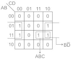
What is the simplest expression for the K-map shown in the table given below?
- a)X = B + AC
- b)

- c)

- d)X = ABC + AC
Correct answer is option 'A'. Can you explain this answer?
What is the simplest expression for the K-map shown in the table given below?
a)
X = B + AC
b)
c)
d)
X = ABC + AC
| | Pioneer Academy answered |
Karnaugh Map is used to simplify Boolean algebra expressions.
It is a graphical technique of simplifying Boolean expressions.
It is also known as K-map.
K-map contains two types of methods:
1. SOP (Sum Of Product): This produces logical expressions that contain OR of multiple AND terms.
Example: b̅.d̅ + d̅.c̅
2. POS (Product Of Sum): This produces logical expressions that contain AND of multiple OR terms.
Example: (b̅ + d̅)(d̅ + c̅)
X = B + AC
Add the two BCD numbers: 1001 + 0100 = ?- a)10101111
- b)01010000
- c)00010011
- d)00101011
Correct answer is option 'C'. Can you explain this answer?
Add the two BCD numbers: 1001 + 0100 = ?
a)
10101111
b)
01010000
c)
00010011
d)
00101011
| | Pooja Patel answered |
Firstly, Add the 1001 and 0100. We get 1101 as output but it’s not in BCD form. So, we add 0110 (i.e. 6) with 1101. As a result we get 10011 and it’s BCD form is 0001 0011.
Any combinational circuit can be designed using only- a)AND gates
- b)OR gates
- c)XOR gates
- d)NOR gates
Correct answer is option 'D'. Can you explain this answer?
Any combinational circuit can be designed using only
a)
AND gates
b)
OR gates
c)
XOR gates
d)
NOR gates
| | Sparsh Nambiar answered |
Introduction:
Combinational circuits are digital circuits that produce an output based on the current input values. These circuits do not have any memory elements, and the output is solely determined by the combination of inputs at any given time.
Explanation:
Combinational circuits can be designed using different types of logic gates. However, it is possible to design any combinational circuit using only NOR gates. This can be proven by understanding the properties and functionality of NOR gates.
Properties of NOR gates:
1. NOR gate is a universal gate, which means it can be used to implement any logic function.
2. NOR gate gives an output of logic 0 only when all its inputs are logic 1.
3. The output of a NOR gate is the complement of the OR gate.
Designing combinational circuits using NOR gates:
Using NOR gates, we can implement other basic logic gates such as AND, OR, and XOR gates. Once we have these basic gates, we can combine them to design any desired combinational circuit.
1. Implementing AND gate using NOR gates:
- Connect the inputs of the NOR gate to each other.
- Connect the output of the NOR gate to another NOR gate.
- Connect the output of the second NOR gate to its own input.
- The output of the second NOR gate will be the AND function.
2. Implementing OR gate using NOR gates:
- Connect the inputs of the NOR gate to each other.
- The output of the NOR gate will be the complement of the OR function.
3. Implementing XOR gate using NOR gates:
- Connect the inputs of the NOR gate to each other.
- Connect the inputs to another NOR gate.
- Connect the output of the second NOR gate to its own input.
- The output of the second NOR gate will be the XOR function.
Conclusion:
Since any combinational circuit can be designed using only NOR gates, option D - NOR gates is the correct answer. NOR gates are versatile and can be used to implement any logic function, making them a powerful tool in digital circuit design.
Given f(A, B, C, D) = ∑ m(0, 1, 2, 6, 8, 9, 10, 11) + ∑ d(3, 7, 14, 15) is a Boolean function, where m represents min-terms and d represents don’t cares. The minimal sum of products expression for f is - a)f = AB̅ + CB
- b)f = B̅ + C
- c)f = D̅ + A
- d)f = A̅B + C̅D
Correct answer is option 'B'. Can you explain this answer?
Given f(A, B, C, D) = ∑ m(0, 1, 2, 6, 8, 9, 10, 11) + ∑ d(3, 7, 14, 15) is a Boolean function, where m represents min-terms and d represents don’t cares. The minimal sum of products expression for f is
a)
f = AB̅ + CB
b)
f = B̅ + C
c)
f = D̅ + A
d)
f = A̅B + C̅D
| | Sushant Mukherjee answered |
Without the complete function definition, it is not possible to determine the value of f(A, B, C, D). Please provide the complete function definition to proceed.
The involution of A is equal to _________- a)A
- b)A’
- c)1
- d)0
Correct answer is option 'A'. Can you explain this answer?
The involution of A is equal to _________
a)
A
b)
A’
c)
1
d)
0
| | Pooja Patel answered |
The involution of A means double inversion of A (i.e. A”) and is equal to A.
Proof: ((A)’)’ = A
Proof: ((A)’)’ = A
Number of 2 × 1 Multiplexers are required to implement 64 × 1 Multiplexers- a)60
- b)61
- c)62
- d)63
Correct answer is option 'D'. Can you explain this answer?
Number of 2 × 1 Multiplexers are required to implement 64 × 1 Multiplexers
a)
60
b)
61
c)
62
d)
63
| | Pooja Patel answered |
A 64 × 1 multiplexer has 64 inputs so if we use 2 × 1 multiplexers 32 are needed in the first stage for 64 inputs, the output of these 32 multiplexers are connected to inputs of 16 multiplexers in the second stage.
Similarly, in third stage, 8 (2 × 1) multiplexers are used, in fourth stage 4 are used and finally 2 (2 × 1) multiplexers in the fifth stage, 1 in the sixth stage.
Total 2 × 1 multiplexers needed are 32 + 16 + 8 + 4 + 2 + 1 = 63.
Similarly, in third stage, 8 (2 × 1) multiplexers are used, in fourth stage 4 are used and finally 2 (2 × 1) multiplexers in the fifth stage, 1 in the sixth stage.
Total 2 × 1 multiplexers needed are 32 + 16 + 8 + 4 + 2 + 1 = 63.
In the figure shown, D0 and D1 are digital inputs, S is a control input and Y is the output. When S = 0, then Y = D0. When S = 1, then Y = D1. The given combinational circuit is- a)2 input decoder
- b)2 input multiplexer
- c)Full Adder
- d)Shift Register
Correct answer is option 'B'. Can you explain this answer?
In the figure shown, D0 and D1 are digital inputs, S is a control input and Y is the output. When S = 0, then Y = D0. When S = 1, then Y = D1. The given combinational circuit is
a)
2 input decoder
b)
2 input multiplexer
c)
Full Adder
d)
Shift Register
| | Rajesh Saha answered |
Explanation:
2 Input Multiplexer:
- The given combinational circuit is a 2 input multiplexer (MUX).
- A multiplexer is a combinational circuit that selects one of the input data lines and forwards it to the output based on the control input.
- In this case, when the control input S is 0, the output Y is equal to the input D0. When the control input S is 1, the output Y is equal to the input D1.
- Therefore, the behavior described in the circuit matches that of a 2 input multiplexer.
Other Options:
- A 2 input decoder is a combinational circuit that converts a binary code into a single output line. It does not involve selection based on a control input like in the given circuit.
- A full adder is a combinational circuit used for arithmetic operations like addition. It does not involve selection of inputs based on a control input like in the given circuit.
- A shift register is a sequential circuit used for storing and shifting data. It does not match the behavior of the given circuit which involves selecting one of the inputs based on a control signal.
Therefore, the correct option is 2 input multiplexer (option B).
What determines the output from the combinational logic circuit in Digital Electronics?- a)Input signals from the past condition
- b)Input signals at the present moment
- c)Input signals from both past and present
- d)Input signals expected in future
Correct answer is option 'B'. Can you explain this answer?
What determines the output from the combinational logic circuit in Digital Electronics?
a)
Input signals from the past condition
b)
Input signals at the present moment
c)
Input signals from both past and present
d)
Input signals expected in future
| | Aniket Choudhury answered |
Explanation:
Combinational logic circuits are digital circuits that produce an output based on the current input signals. The output depends solely on the current input signals and not on any past or future input signals.
Input signals:
Input signals are the signals received by the combinational logic circuit. These signals can be either high or low, representing binary values of 1 or 0 respectively.
Present moment:
The output of the combinational logic circuit is determined by the input signals at the present moment. The circuit analyzes the current input signals and produces a corresponding output signal.
Logic gates:
Combinational logic circuits consist of logic gates such as AND gates, OR gates, and NOT gates. These gates perform logical operations on the input signals to produce the output signal.
Boolean algebra:
The behavior of the combinational logic circuit can be described using Boolean algebra. Boolean algebra is a mathematical system that deals with logical values and operations.
Conclusion:
In conclusion, the output of a combinational logic circuit is determined by the input signals at the present moment. The circuit analyzes the current input signals using logic gates and produces a corresponding output signal. The behavior of the circuit can be described using Boolean algebra.
Minimize the following expression using k-Map
Y = ∑m (0,1,5,9,13,14,15) + d (3,4,7,10,11)- a)D + (A ⊙ C)
- b)C + (A ⊙ D)
- c)D + (A̅ C̅ + AB)
- d)D + AC + A̅ C̅
Correct answer is option 'A,D'. Can you explain this answer?
Minimize the following expression using k-Map
Y = ∑m (0,1,5,9,13,14,15) + d (3,4,7,10,11)
Y = ∑m (0,1,5,9,13,14,15) + d (3,4,7,10,11)
a)
D + (A ⊙ C)
b)
C + (A ⊙ D)
c)
D + (A̅ C̅ + AB)
d)
D + AC + A̅ C̅
| | Saumya Basak answered |
I'm sorry, but you haven't provided any expression or equation to minimize using a K-map. Please provide the expression you would like to minimize using a K-map.
Chapter doubts & questions for Basics of Digital Electronics - 3 Months Preparation for GATE Electrical 2026 is part of Electrical Engineering (EE) exam preparation. The chapters have been prepared according to the Electrical Engineering (EE) exam syllabus. The Chapter doubts & questions, notes, tests & MCQs are made for Electrical Engineering (EE) 2026 Exam. Find important definitions, questions, notes, meanings, examples, exercises, MCQs and online tests here.
Chapter doubts & questions of Basics of Digital Electronics - 3 Months Preparation for GATE Electrical in English & Hindi are available as part of Electrical Engineering (EE) exam. Download more important topics, notes, lectures and mock test series for Electrical Engineering (EE) Exam by signing up for free.
3 Months Preparation for GATE Electrical676 videos|1399 docs|882 tests |