


All Exams > NEET > 30-Day Revision Course for NEET > All Questions
All questions of Semiconductors for NEET Exam


The device that can act as a complete electroniccircuit is [2010]- a)junction diode
- b)integrated circuit
- c)junction transistor
- d)zener diode
Correct answer is option 'B'. Can you explain this answer?
The device that can act as a complete electroniccircuit is [2010]
a)
junction diode
b)
integrated circuit
c)
junction transistor
d)
zener diode
 | Rajeev Sharma answered |
Integrated circuit can act as a complete
electronic circuit.
electronic circuit.
In a semiconductor crystal, if current flows due to breakage of crystal bonds, then the semiconductor is called- a)donor
- b)acceptor
- c)extrinsic semiconductor
- d)intrinsic semiconductor
Correct answer is option 'D'. Can you explain this answer?
In a semiconductor crystal, if current flows due to breakage of crystal bonds, then the semiconductor is called
a)
donor
b)
acceptor
c)
extrinsic semiconductor
d)
intrinsic semiconductor
| | Preeti Iyer answered |
In the case of an intrinsic semiconductor (say Si) where each Si is having 4 outermost electrons, its crystal structure consists of making 4 covalent bonds with 4 neighbouring Si atoms. Each bond consists of two electrons.
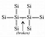
Now if one of the bonds gets broken due to some reason (collisions or high temperature) then one electron gets free and it will be having sufficient energy to cross the band gap and be ready for conduction- So in intrinsic semiconductors, current flows due to breakage of crystal bonds.
Now if one of the bonds gets broken due to some reason (collisions or high temperature) then one electron gets free and it will be having sufficient energy to cross the band gap and be ready for conduction- So in intrinsic semiconductors, current flows due to breakage of crystal bonds.
Which one of the following bonds produces asolid that reflects light in the visible region andwhose electrical conductivity decreases withtemperature and has high melting point? [2010]- a)metallic bonding
- b)van der Waal's bonding
- c)ionic bonding
- d)covalent bonding
Correct answer is option 'A'. Can you explain this answer?
Which one of the following bonds produces asolid that reflects light in the visible region andwhose electrical conductivity decreases withtemperature and has high melting point? [2010]
a)
metallic bonding
b)
van der Waal's bonding
c)
ionic bonding
d)
covalent bonding
 | Naveen Menon answered |
For a metal, conductivity decreases with
increase in temperature.
Also, metal has high melting point.
increase in temperature.
Also, metal has high melting point.


The conductivity of P – type semiconductor is due to- a)both electrons and holes
- b)holes
- c)electrons
- d)none of the above.
Correct answer is option 'B'. Can you explain this answer?
The conductivity of P – type semiconductor is due to
a)
both electrons and holes
b)
holes
c)
electrons
d)
none of the above.
| | Lavanya Menon answered |
A P-type semiconductor is formed when a trivalent electron deficient impurities such as boron group elements are doped with intrinsic semiconductor. As the impurities are electron deficient, they take electrons from the valence band creating a number of holes. Due this reason conductivity in P-type semiconductor is mainly due to holes rather than electrons.
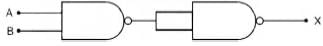
Symbolic representation of four logic gate are shown as [2011]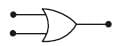
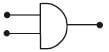
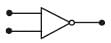
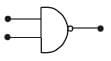 Pick out which ones are for AND, NAND and NOT gates, respectively
- a)(ii), (iii) and (iv)
- b)(iii), (ii) and (i)
- c)(iii), (iii) and (iv)
- d)(ii), (iv) and (iii)
Correct answer is option 'D'. Can you explain this answer?
Symbolic representation of four logic gate are shown as [2011]
Pick out which ones are for AND, NAND and NOT gates, respectively
a)
(ii), (iii) and (iv)
b)
(iii), (ii) and (i)
c)
(iii), (iii) and (iv)
d)
(ii), (iv) and (iii)
| | Ayaan Madhukar answered |
Simple bro...
Correct answer is option (D)...
Correct answer is option (D)...
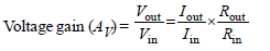
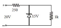
The input resistance of a silicon transistor is100 W. Base current is changed by 40 μA whichresults in a change in collector current by 2 mA.This transistor is used as a common emitteramplifier with a load resistance of 4 KΩ. Thevoltage gain of the amplifier is : [2012M]- a)2000
- b)3000
- c)4000
- d)1000
Correct answer is option 'A'. Can you explain this answer?
The input resistance of a silicon transistor is100 W. Base current is changed by 40 μA whichresults in a change in collector current by 2 mA.This transistor is used as a common emitteramplifier with a load resistance of 4 KΩ. Thevoltage gain of the amplifier is : [2012M]
a)
2000
b)
3000
c)
4000
d)
1000
 | Prasenjit Pillai answered |
A solid having uppermost energy – band partially filled with electrons is called- a)none of the above
- b)a conductor
- c)a semi – conductor
- d)an insulator
Correct answer is option 'B'. Can you explain this answer?
A solid having uppermost energy – band partially filled with electrons is called
a)
none of the above
b)
a conductor
c)
a semi – conductor
d)
an insulator
| | Riya Banerjee answered |
Conductor is an object or type of material that allows the flow of an electrical current in one more directions. A metal wire is a common electrical conductor. In metals such as copper or aluminium, the mobile charged particles are welcome.
An N-type Ge is obtained on doping the Ge- crystal with- a)boron
- b)gold
- c)aluminum
- d)phosphorus
Correct answer is option 'D'. Can you explain this answer?
An N-type Ge is obtained on doping the Ge- crystal with
a)
boron
b)
gold
c)
aluminum
d)
phosphorus
 | Ishani Patel answered |
Explanation:The addition of pentavalent impurities such as antimony, arsenic or phosphorous contributes free electrons, greatly increasing the conductivity of the intrinsic semiconductor.
Hole is- a)An anti-particle of electron
- b)An artifically created particle
- c)Absence of free electrons
- d)A vacancy created when an electron leaves a covalent bond
Correct answer is option 'D'. Can you explain this answer?
Hole is
a)
An anti-particle of electron
b)
An artifically created particle
c)
Absence of free electrons
d)
A vacancy created when an electron leaves a covalent bond
| | Zeal Gosai answered |
Actually hole is not anything we just asume that when an electron moves it creates a vacancy which we call a hole.
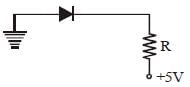
In a p-n junction, as the diffusion process continues the width of the depletion zone- a)decreases
- b)increases
- c)remains the same
- d)oscillates
Correct answer is option 'B'. Can you explain this answer?
In a p-n junction, as the diffusion process continues the width of the depletion zone
a)
decreases
b)
increases
c)
remains the same
d)
oscillates
| | Preeti Iyer answered |
In reverse biasing, the positive terminal of the battery is connected to the n-type whereas the negative terminal is connected to the p-type junction. So the positive terminal tends to pull the electrons (near to the depletion layer) in n-type towards itself whereas the negative terminal pulls the holes towards itself which results in an increase in the width of the depletion layer.
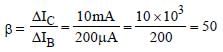
In a CE transistor amplifier, the audio signalvoltage across the collector resistance of 2kΩ is 2V. If the base resistance is 1kΩ and thecurrent amplification of the transistor is 100, theinput signal voltage is : [2012]- a)0.1 V
- b)1.0 V
- c)1 mV
- d)10 mV
Correct answer is option 'D'. Can you explain this answer?
In a CE transistor amplifier, the audio signalvoltage across the collector resistance of 2kΩ is 2V. If the base resistance is 1kΩ and thecurrent amplification of the transistor is 100, theinput signal voltage is : [2012]
a)
0.1 V
b)
1.0 V
c)
1 mV
d)
10 mV
 | Ishaan Menon answered |
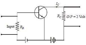
The output voltage, across the load RC
V0 = IC RC = 2
The collector current (IC)
V0 = IC RC = 2
The collector current (IC)
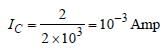
Current gain (β)
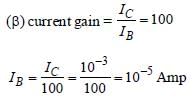
Input voltage (Vi)
Vi = RB IB = 1 × 10, × 10–5 = 10–2 Volt
Vi = 10 mV
Vi = RB IB = 1 × 10, × 10–5 = 10–2 Volt
Vi = 10 mV
When the conductivity of a semiconductor is only due to breaking of the covalent bonds, the semiconductor is called- a)donor
- b)acceptor
- c)intrinsic
- d)extrinsic
Correct answer is option 'C'. Can you explain this answer?
When the conductivity of a semiconductor is only due to breaking of the covalent bonds, the semiconductor is called
a)
donor
b)
acceptor
c)
intrinsic
d)
extrinsic
 | Arpita Nair answered |
Explanation:A pure semiconductor is called intrinsic semiconductor, e.g., silicon, germanium. The presence of the mobile charge carriers is the intrinsic property of the material. At room temperature, some covalent bonds are broken and electrons are made free. The absence of electron in the covalent bond form hole.The electrical conduction is by means of mobile electrons and holes. Hole act as positive charge, because it can attract an electron. If some other bond is broken and the electron thus freed fills this hole(vacancy), it seems as though the hole is moving.Actually an electron is travelling in opposite direction. In a pure(intrinsic) semiconductor, the number of holes is equal to the number of free electrons.
When a P- N junction is reversed biased, the flow of current across the junction is mainly due to- a)both drift and diffusion of the charges
- b)depends upon the nature of material.
- c)diffusion of charge carriers
- d)drift of charges
Correct answer is option 'D'. Can you explain this answer?
When a P- N junction is reversed biased, the flow of current across the junction is mainly due to
a)
both drift and diffusion of the charges
b)
depends upon the nature of material.
c)
diffusion of charge carriers
d)
drift of charges
| | Upasana Sen answered |
When p-n junction is reverse biased, the flow of current is due to drifting of minority charge carriers across the junction.
When n –type of semiconductor is heated- a)number of electrons increases while that of holes decreases
- b)number of electrons and holes increases equally
- c)number of holes increases while that of electrons is same
- d)number of electrons and holes remains same
Correct answer is option 'B'. Can you explain this answer?
When n –type of semiconductor is heated
a)
number of electrons increases while that of holes decreases
b)
number of electrons and holes increases equally
c)
number of holes increases while that of electrons is same
d)
number of electrons and holes remains same
 | Gauri Khanna answered |
Explanation:Due to heating, when a free electron is produced then simultaneously a hole is also produced.
In the middle of the depletion layer of a reverse biased p-n-junction, the- a)potential is maximum
- b)electric field is maximum
- c)electric field is zero
- d)potential is zero
Correct answer is option 'C'. Can you explain this answer?
In the middle of the depletion layer of a reverse biased p-n-junction, the
a)
potential is maximum
b)
electric field is maximum
c)
electric field is zero
d)
potential is zero
| | Vijay Bansal answered |
Due to the reverse biasing the width of depletion region increases and current flowing through the diode is almost zero. In this case electric field is almost zero at the middle of the depletion region.
Basic materials used in the present solid state electronic devices like diode, transistor, ICs, etc are- a)Semiconductors
- b)metals
- c)insulators
- d)conductors
Correct answer is option 'A'. Can you explain this answer?
Basic materials used in the present solid state electronic devices like diode, transistor, ICs, etc are
a)
Semiconductors
b)
metals
c)
insulators
d)
conductors
 | Keerthana Mehta answered |
Explanation:Semiconductors are materials that have electrical conductivity between conductors such as most metals and nonconductors or insulators like ceramics. Semiconductor material is used in the manufacturing of electrical components and used in electronic devices such as transistors and diodes.Semiconductors are the basic materials used in the present solid state electronic devices like diode, transistor, ICs etc
Which of the following is not a semiconductor?- a)Germanium
- b)Selenium
- c)Radium
- d)Silicon
Correct answer is option 'C'. Can you explain this answer?
Which of the following is not a semiconductor?
a)
Germanium
b)
Selenium
c)
Radium
d)
Silicon
 | Rishika Chauhan answered |
Explanation:Materials that have the resistance levels between those of a conductor and an insulator are referred to as semiconductors.They are quite common, found in almost all electronic devices. Good examples of semiconductor materials are germanium, selenium, and silicon.Radium is a chemical element with symbol Ra and atomic number 88. It is the sixth element in group 2 of the periodic table, also known as the alkaline earth metals.
In a pure, or intrinsic, semiconductor, valence band holes and conduction-band electrons are always present- a)such that number of holes is greater than the number of electrons
- b)in equal numbers
- c)such that number of electrons is greater than the number of holes
- d)none of these
Correct answer is option 'B'. Can you explain this answer?
In a pure, or intrinsic, semiconductor, valence band holes and conduction-band electrons are always present
a)
such that number of holes is greater than the number of electrons
b)
in equal numbers
c)
such that number of electrons is greater than the number of holes
d)
none of these
 | Sinjini Tiwari answered |
Explanation:An intrinsic semiconductor, also called an undoped semiconductor or i-type semiconductor, is a pure semiconductor without any significant dopant species present. The number of charge carriers is therefore determined by the properties of the material itself instead of the amount of impurities. In intrinsic semiconductors the number of excited electrons and the number of holes are equal: n = p.
In the following figure, the diodes which are forward biased, are [2011M]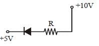
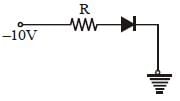

- a)(C) only
- b)(C) and (A)
- c)(B) and (D)
- d)(A), (B) and (D)
Correct answer is option 'B'. Can you explain this answer?
In the following figure, the diodes which are forward biased, are [2011M]
a)
(C) only
b)
(C) and (A)
c)
(B) and (D)
d)
(A), (B) and (D)
 | Abhijeet Goyal answered |
Only in (A) and (C) diodes are forward biased
as p-type should be at higher potential and
n-type at lower potential.
as p-type should be at higher potential and
n-type at lower potential.
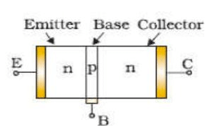
For transistor action :
(1) Base, emitter and collector regions should have similar size and doping concentrations.
(2) The base region must be very thin and lightly doped.
(3) The eimtter-base junction is forward biased and base-collector junction is reverse based.
(4) Both the emitter-base junction as well as the base-collector junction are forward biased.- a)(3), (4)
- b)(4), (1)
- c)(1), (2)
- d)(2), (3)
Correct answer is option 'D'. Can you explain this answer?
For transistor action :
(1) Base, emitter and collector regions should have similar size and doping concentrations.
(2) The base region must be very thin and lightly doped.
(3) The eimtter-base junction is forward biased and base-collector junction is reverse based.
(4) Both the emitter-base junction as well as the base-collector junction are forward biased.
a)
(3), (4)
b)
(4), (1)
c)
(1), (2)
d)
(2), (3)
 | Kunal Rane answered |
For transistor action, the base region must
be very thin and lightly doped. Also, the
emitter-base junction is forward biased and
base-collector junction is reverse biased
be very thin and lightly doped. Also, the
emitter-base junction is forward biased and
base-collector junction is reverse biased
In forward biasing of the p–n junction [2011]- a)the positive terminal of the battery isconnected to p–side and the depletionregion becomes thick
- b)the positive terminal of the battery isconnected to n–side and the depletionregion becomes thin
- c)the positive terminal of the battery isconnected to n–side and the depletionregion becomes thick
- d)the positive terminal of the battery isconnected to p–side and the depletionregion becomes thin
Correct answer is option 'D'. Can you explain this answer?
In forward biasing of the p–n junction [2011]
a)
the positive terminal of the battery isconnected to p–side and the depletionregion becomes thick
b)
the positive terminal of the battery isconnected to n–side and the depletionregion becomes thin
c)
the positive terminal of the battery isconnected to n–side and the depletionregion becomes thick
d)
the positive terminal of the battery isconnected to p–side and the depletionregion becomes thin
 | Ayush Chavan answered |
In forward biasing of the p-n junction, the
positive terminal of the battery is connected
to p-side and the negative terminal of the
battery is connected to n-side. The depletion
region becomes thin.
positive terminal of the battery is connected
to p-side and the negative terminal of the
battery is connected to n-side. The depletion
region becomes thin.
The depletion layer in the p-n junction is caused- a)drift of electrons
- b)drift of holes
- c)migration of impurity ions
- d)diffusion of carrier ions
Correct answer is option 'D'. Can you explain this answer?
The depletion layer in the p-n junction is caused
a)
drift of electrons
b)
drift of holes
c)
migration of impurity ions
d)
diffusion of carrier ions
| | Madhurima Mishra answered |
Depletion Layer in the p-n Junction
The p-n junction is a key component in various electronic devices such as diodes and transistors. It is formed by bringing together a p-type semiconductor (which has an excess of holes) and an n-type semiconductor (which has an excess of electrons). When these two materials are joined, a depletion layer is formed at the interface between them.
The depletion layer is a region in the p-n junction where there are no free charge carriers (electrons or holes). It is caused by a combination of diffusion and electric field effects. The depletion layer plays a crucial role in the operation of the p-n junction.
Diffusion of Carrier Ions
One of the main factors contributing to the formation of the depletion layer is the diffusion of carrier ions. In the p-type region, where there is an excess of holes, some of these holes will diffuse across the junction into the n-type region. Similarly, in the n-type region, some of the excess electrons will diffuse into the p-type region.
This diffusion process continues until an equilibrium is reached, where the concentration of carrier ions is equal on both sides of the junction. As a result, a region is formed near the junction that is depleted of carriers, hence the name "depletion layer."
Electric Field Effects
In addition to diffusion, the formation of the depletion layer is also influenced by electric field effects. When the p-n junction is formed, the excess holes in the p-region and excess electrons in the n-region create an electric field that opposes further diffusion of carriers.
This electric field acts as a barrier to the diffusion of holes from the p-region to the n-region and electrons from the n-region to the p-region. As a result, the depletion layer widens and the electric field strength increases, creating a potential barrier that prevents the flow of current in the absence of an external bias.
Conclusion
In summary, the depletion layer in the p-n junction is primarily caused by the diffusion of carrier ions. The excess carriers in the p-type and n-type regions diffuse across the junction, leading to the formation of a region depleted of carriers. The electric field effects also contribute to the widening of the depletion layer by opposing further carrier diffusion. Understanding the formation and characteristics of the depletion layer is essential in analyzing the behavior and functionality of p-n junction devices.
Pure Si at 500K has equal number ofelectron (ne) and hole (nh) concentrations of1.5 × 1016 m–3. Doping by indium increases nhto 4.5 × 10²² m–3. The doped semiconductor isof [2011M]- a)n–type with electron concentrationne = 5 × 10²² m–3
- b)p–type with electron concentrationne = 2.5 ×10¹⁰ m–3
- c)n–type with electron concentrationne = 2.5 × 10²³ m–3
- d)p–type having electron concentrationne = 5 × 10⁹ m–3
Correct answer is option 'D'. Can you explain this answer?
Pure Si at 500K has equal number ofelectron (ne) and hole (nh) concentrations of1.5 × 1016 m–3. Doping by indium increases nhto 4.5 × 10²² m–3. The doped semiconductor isof [2011M]
a)
n–type with electron concentrationne = 5 × 10²² m–3
b)
p–type with electron concentrationne = 2.5 ×10¹⁰ m–3
c)
n–type with electron concentrationne = 2.5 × 10²³ m–3
d)
p–type having electron concentrationne = 5 × 10⁹ m–3
 | Deepak Joshi answered |
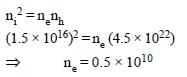
or ne = 5 × 10⁹
Given nh = 4.5 × 10²²
⇒nh >> ne
∴ Semiconductor is p-type and
ne = 5 × 10⁹ m–3.
Given nh = 4.5 × 10²²
⇒nh >> ne
∴ Semiconductor is p-type and
ne = 5 × 10⁹ m–3.
In a common emitter (CE) amplifier having a voltage gain G, the transistor used has transconductance 0.03 mho and current gain 25. If the above transistor is replaced with another one with transconductance 0.02 mho and current gain 20, the voltage gain will be [NEET 2013] - a)1.5 G
- b)1/3 G
- c)5/4 G
- d)2/3 G
Correct answer is option 'D'. Can you explain this answer?
In a common emitter (CE) amplifier having a voltage gain G, the transistor used has transconductance 0.03 mho and current gain 25. If the above transistor is replaced with another one with transconductance 0.02 mho and current gain 20, the voltage gain will be [NEET 2013]
a)
1.5 G
b)
1/3 G
c)
5/4 G
d)
2/3 G
| | Isha Rane answered |
Given:
Transconductance of 1st transistor (gm1) = 0.03 mho
Current gain of 1st transistor (β1) = 25
Voltage gain of Common Emitter amplifier = G
To Find:
Voltage gain of Common Emitter amplifier when the transistor is replaced with another one with gm2 = 0.02 mho and β2 = 20
Solution:
We know that the voltage gain of a common emitter amplifier is given by the formula:
G = -gm * R_c * β
Where gm is the transconductance of the transistor, Rc is the collector resistance and β is the current gain.
Let's assume that the collector resistance remains the same in both cases. Therefore, we can write:
G1 = -gm1 * Rc * β1
G2 = -gm2 * Rc * β2
Dividing G2 by G1, we get:
G2/G1 = (-gm2 * Rc * β2) / (-gm1 * Rc * β1)
Simplifying the above equation, we get:
G2/G1 = (gm1/gm2) * (β2/β1)
Substituting the given values, we get:
G2/G1 = (0.03/0.02) * (20/25) = 0.9
Therefore, the voltage gain of the common emitter amplifier when the transistor is replaced with another one with gm2 = 0.02 mho and β2 = 20 is:
G2 = G1 * (G2/G1) = G * 0.9
G2 = 0.9G
Hence, the correct option is (d) 2/3 G.
The main difference between conductors, semiconductors and insulators is because of- a)Work function
- b)Mobility of electrons
- c)Energy of electrons
- d)Width of forbidden energy gap
Correct answer is option 'D'. Can you explain this answer?
The main difference between conductors, semiconductors and insulators is because of
a)
Work function
b)
Mobility of electrons
c)
Energy of electrons
d)
Width of forbidden energy gap
| | Niti Saha answered |
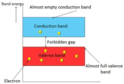
Explanation:Forbidden gap plays a major role for determining the electrical conductivity of material. Based on the forbidden gap materials are classified in to three types, they are : Insulators : The forbidden gap between the valence band and conduction band is very large in insulators. The energy gap of insulator is approximately equal to 15 electron volts (eV).Conductors: In a conductor, valence band and conduction band overlap each other. Therefore, there is no forbidden gap in a conductor.Semiconductors: In semiconductors, the forbidden gap between valence band and conduction band is very small. It has a forbidden gap of about 1 electron volt (eV).
In the case of metals the valence and conduction bands have- a)no overlap, energy gap is large
- b)no overlap, energy gap is small
- c)overlap, energy gap =0
- d)no overlap, energy gap =0
Correct answer is option 'C'. Can you explain this answer?
In the case of metals the valence and conduction bands have
a)
no overlap, energy gap is large
b)
no overlap, energy gap is small
c)
overlap, energy gap =0
d)
no overlap, energy gap =0
 | Yash Kumar answered |
Explanation:
In the case of metals, the valence and conduction bands have an overlap, and the energy gap between them is zero.
1. Valence Band:
- The valence band is the highest energy band that is fully occupied by electrons in a material at absolute zero temperature.
- It consists of the valence electrons, which are tightly bound to the atomic nuclei.
- These electrons are not free to move and contribute to the electrical conductivity of the material.
2. Conduction Band:
- The conduction band is the energy band located just above the valence band.
- It contains empty or partially filled energy states that are available for electrons to move freely and contribute to the electrical conductivity of the material.
- Electrons in the conduction band have higher energy and are not bound to any specific atom.
3. Energy Gap:
- The energy gap is the energy difference between the valence and conduction bands.
- In insulators, this gap is large, typically on the order of several electron volts, which makes it difficult for electrons to move from the valence band to the conduction band.
- In semiconductors, the energy gap is smaller than in insulators, allowing some electrons to acquire enough energy to move from the valence band to the conduction band, contributing to electrical conductivity.
- In metals, the energy gap between the valence and conduction bands is zero, meaning that there is no energy barrier for electrons to move from the valence band to the conduction band.
- This overlap allows electrons to move freely throughout the material, resulting in high electrical conductivity.
Conclusion:
In summary, in the case of metals, the valence and conduction bands have an overlap, and the energy gap between them is zero. This overlap allows electrons to move freely, contributing to the high electrical conductivity observed in metals.
Doping of semiconductor is the process of- a)adding a surface coating
- b)adding impurity to pure semiconductor
- c)removing impurity from pure semiconductor
- d)None of these
Correct answer is option 'B'. Can you explain this answer?
Doping of semiconductor is the process of
a)
adding a surface coating
b)
adding impurity to pure semiconductor
c)
removing impurity from pure semiconductor
d)
None of these
 | Mehul Choudhary answered |
Doping of Semiconductors
Doping is a fundamental process in semiconductor technology that enhances the electrical properties of pure semiconductors. Here's a detailed explanation of the process:
What is Doping?
- Doping refers to the intentional introduction of impurities into a pure semiconductor material.
- The primary purpose is to modify the electrical characteristics, enhancing conductivity.
Types of Doping
- N-Type Doping:
- Involves adding elements with extra electrons, such as phosphorus or arsenic, to silicon.
- This process increases the number of free electrons, enhancing the material's conductivity.
- P-Type Doping:
- Involves adding elements that create "holes" or positive charge carriers, such as boron.
- This results in a deficiency of electrons, allowing positive charge carriers to dominate.
Significance of Doping
- Doping allows for the control of the electrical properties of semiconductors, enabling them to be used in various electronic devices.
- It is crucial for the manufacturing of diodes, transistors, and integrated circuits.
Conclusion
- The correct answer to the question of what doping is pertains to option 'B': adding impurity to pure semiconductor.
- This process is essential for tailoring semiconductor materials to meet specific electronic requirements and enhance their functionality.
A p- type semiconductor can be obtained by adding- a)gallium to pure silicon
- b)phosphorus to pure germanium
- c)arsenic to pure silicon
- d)antimony to pure germanium
Correct answer is option 'A'. Can you explain this answer?
A p- type semiconductor can be obtained by adding
a)
gallium to pure silicon
b)
phosphorus to pure germanium
c)
arsenic to pure silicon
d)
antimony to pure germanium
 | Gauri Sharma answered |
Explanation:In P-type doping, boron or gallium is the dopant. Boron and gallium each have only three outer electrons. When mixed into the silicon lattice, they form "holes" in the lattice where a silicon electron has nothing to bond to. The absence of an electron creates the effect of a positive charge, hence the name P-type.Holes can conduct current. A hole happily accepts an electron from a neighbor, moving the hole over a space. P-type silicon is a good conductor.
C and Si both have same lattice structure, having 4 bonding electrons in each. However, C isinsulator whereas Si is intrinsic semiconductor.This is because : [2012]- a)In case of C the valence band is notcompletely filled at absolute zerotemperature.
- b)In case of C the conduction band is partlyfilled even at absolute zero temperature.
- c)The four bonding electrons in the case of Clie in the second orbit, whereas in the caseof Si they lie in the third.
- d)The four bonding electrons in the case of Clie in the third orbit, whereas for Si they liein the fourth orbit.
Correct answer is option 'C'. Can you explain this answer?
C and Si both have same lattice structure, having 4 bonding electrons in each. However, C isinsulator whereas Si is intrinsic semiconductor.This is because : [2012]
a)
In case of C the valence band is notcompletely filled at absolute zerotemperature.
b)
In case of C the conduction band is partlyfilled even at absolute zero temperature.
c)
The four bonding electrons in the case of Clie in the second orbit, whereas in the caseof Si they lie in the third.
d)
The four bonding electrons in the case of Clie in the third orbit, whereas for Si they liein the fourth orbit.
| | Subhankar Choudhary answered |
Explanation:
C and Si have the same lattice structure, but their electrical properties are different. The reason for this difference lies in the electronic configuration of the two elements.
Valence electrons
Both C and Si have 4 valence electrons, which are involved in bonding. The electronic configuration of C is 1s2 2s2 2p2, while that of Si is 1s2 2s2 2p6 3s2 3p2. This means that the valence electrons of C lie in the second orbit, whereas those of Si lie in the third orbit.
Bonding
The valence electrons of C and Si are involved in covalent bonding, which means that they share electrons with their neighboring atoms. In the case of C, each atom forms 4 covalent bonds, resulting in a very stable structure. However, this stable structure also means that the valence band is not completely filled at absolute zero temperature. Therefore, C is an insulator.
Intrinsic semiconductor
On the other hand, Si is an intrinsic semiconductor because its valence band is completely filled at absolute zero temperature, but there is a small energy gap between the valence band and the conduction band. This energy gap is small enough that thermal energy can cause electrons to jump from the valence band to the conduction band, allowing the material to conduct electricity. This property of semiconductors is utilized in many electronic devices.
Conclusion
In summary, the difference in electronic configuration between C and Si leads to differences in their electrical properties. While C is an insulator due to the incomplete filling of its valence band, Si is an intrinsic semiconductor due to the small energy gap between its valence and conduction bands.
In a n-type semiconductor, which of the followingstatement is true? [NEET 2013]- a)Electrons are minority carriers andpentavalent atoms are dopants.
- b)Holes are minority carriers and pentavalentatoms are dopants.
- c)Holes are majority carriers and trivalentatoms are dopants.
- d)Electrons are majority carriers and trivalentatoms are dopants.
Correct answer is option 'B'. Can you explain this answer?
In a n-type semiconductor, which of the followingstatement is true? [NEET 2013]
a)
Electrons are minority carriers andpentavalent atoms are dopants.
b)
Holes are minority carriers and pentavalentatoms are dopants.
c)
Holes are majority carriers and trivalentatoms are dopants.
d)
Electrons are majority carriers and trivalentatoms are dopants.
| | Ayush Chavan answered |
In a n-type semiconductor holes are
minority carriers and pentavalent atoms
are dopants.
minority carriers and pentavalent atoms
are dopants.
If a small amount of antimony is added togermanium crystal [2011]- a)it becomes a p–type semiconductor
- b)the antimony becomes an acceptor atom
- c)there will be more free electrons than holesin the semiconductor
- d)its resistance is increased
Correct answer is option 'C'. Can you explain this answer?
If a small amount of antimony is added togermanium crystal [2011]
a)
it becomes a p–type semiconductor
b)
the antimony becomes an acceptor atom
c)
there will be more free electrons than holesin the semiconductor
d)
its resistance is increased
 | Rohan Unni answered |
When small amount of antimony
(pentavalent) is added to germanium crystal
then crystal becomes n-type semi conductor.
Therefore, there will be more free electrons
than holes in the semiconductor.
(pentavalent) is added to germanium crystal
then crystal becomes n-type semi conductor.
Therefore, there will be more free electrons
than holes in the semiconductor.
Transfer characteristics [output voltage (V0) vs input voltage (V1)] for a base biased transistor in CE configuration is as shown in the figure. For using transistor as a switch, it is used : [2012]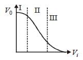
- a)in region III
- b)both in region (I) and (III)
- c)in region II
- d)in region (I)
Correct answer is option 'B'. Can you explain this answer?
Transfer characteristics [output voltage (V0) vs input voltage (V1)] for a base biased transistor in CE configuration is as shown in the figure. For using transistor as a switch, it is used : [2012]
a)
in region III
b)
both in region (I) and (III)
c)
in region II
d)
in region (I)
| | Kunal Rane answered |
I → ON
II → OFF
In IInd state it is used as a amplifier it is
active region
II → OFF
In IInd state it is used as a amplifier it is
active region
A transistor is operated in common emitterconfiguration at VC = 2V such that a change inthe base current from 100 μA to 300 μA producesa change in the collector current from 10mA to20 mA. The current gain is [2011]- a)50
- b)75
- c)100
- d)25
Correct answer is option 'A'. Can you explain this answer?
A transistor is operated in common emitterconfiguration at VC = 2V such that a change inthe base current from 100 μA to 300 μA producesa change in the collector current from 10mA to20 mA. The current gain is [2011]
a)
50
b)
75
c)
100
d)
25
| | Prasenjit Pillai answered |
The current gain
Majority current carriers in N – types are- a)holes
- b)negative ions
- c)positive ions
- d)electrons
Correct answer is option 'D'. Can you explain this answer?
Majority current carriers in N – types are
a)
holes
b)
negative ions
c)
positive ions
d)
electrons
 | Anjali Reddy answered |
Explanation:The more abundant charge carriers are called majority carriers, which are primarily responsible for current transport in a piece of semiconductor. In n-type semiconductors they are electrons, while in p-type semiconductors they are holes.
The difference in variation of resistance with temperature in a metal and semiconductor is due to- a)type of bonding
- b)crystal structure
- c)variation of scattering with temperature
- d)variation in number of charge carries with temperature
Correct answer is option 'D'. Can you explain this answer?
The difference in variation of resistance with temperature in a metal and semiconductor is due to
a)
type of bonding
b)
crystal structure
c)
variation of scattering with temperature
d)
variation in number of charge carries with temperature
| | Shraddha Choudhury answered |
In metals, scattering increases with temperature and hence the flow of electrons is restricted. In semiconductors, the number of charge carriers increases with temperature which overcomes the effect of increasing scattering and hence the resistivity of semiconductors decreases with an increase in temperature but that of metals increases.
A piece of copper and another of germanium are cooled from room temperature to 80 K. The resistance of- a)copper decreases and that of germanium increases
- b)each of them increases
- c)each of them decreases
- d)copper increases and that of germanium decreases
Correct answer is option 'A'. Can you explain this answer?
A piece of copper and another of germanium are cooled from room temperature to 80 K. The resistance of
a)
copper decreases and that of germanium increases
b)
each of them increases
c)
each of them decreases
d)
copper increases and that of germanium decreases
| | Geetika Tiwari answered |
We know, a piece of copper is a metal while that of germanium is a semiconducting material. For metals resistance increases with increase in temperature. The semiconductor has a negative temperature coefficient of resistance. Hence, when it is cooled its resistance increases.
Motion of hole is a convenient way of describing- a)the actual motion of bound electrons
- b)the actual motion of energy gap
- c)the actual motion of free electrons
- d)the actual motion of conduction electrons
Correct answer is option 'A'. Can you explain this answer?
Motion of hole is a convenient way of describing
a)
the actual motion of bound electrons
b)
the actual motion of energy gap
c)
the actual motion of free electrons
d)
the actual motion of conduction electrons
| | Anjali Reddy answered |
Explanation:The holes are just the abscence of a electron in a energy band. But its easier to describe the abscence of a electron as a single moving positive charge than it is to describe the motion of all the other electrons in the band.In a band you have N electrons. Remove one of those electrons(by for instance p-doping) and you have N-1 electrons left. Now you can either choose to describe this with the behavior of those N-1 electrons. Or you can choose to describe it as if there is one single hole moving around in the band.So mathematicly the holes behave just like a positivly charged electron.
In a semiconductor, the forbidden energy gap between the valance band and the conduction band is of the order of- a)1 ev
- b)1 MeV
- c)5 eV
- d)1 GeV
Correct answer is option 'A'. Can you explain this answer?
In a semiconductor, the forbidden energy gap between the valance band and the conduction band is of the order of
a)
1 ev
b)
1 MeV
c)
5 eV
d)
1 GeV
 | Sankar Gupta answered |
Explanation:The material which has electrical conductivity between that of a conductor and an insulator is called as semiconductor. Silicon, germanium and graphite are some examples of semiconductors.
In semiconductors, the forbidden gap between valence band and conduction band is very small. It has a forbidden gap of about 1 electron volt (eV).
Depletion region (space charge) is formed because- a)majority carriers while diffusing to the other side leave behind immobile ionized atoms
- b)majority carriers while drifting to the other side leave behind immobile ionized atoms
- c)majority carriers while diffusing to the other side leave behind highly mobile ionized atoms
- d)minority carriers while diffusing to the other side leave behind immobile ionized atoms
Correct answer is option 'A'. Can you explain this answer?
Depletion region (space charge) is formed because
a)
majority carriers while diffusing to the other side leave behind immobile ionized atoms
b)
majority carriers while drifting to the other side leave behind immobile ionized atoms
c)
majority carriers while diffusing to the other side leave behind highly mobile ionized atoms
d)
minority carriers while diffusing to the other side leave behind immobile ionized atoms
| | Sankar Gupta answered |
Explanation:The depletion region, also called depletion layer, depletion zone, junction region, space charge region or space charge layer, is an insulating region within a conductive, doped semiconductor material where the mobile charge carriers have been diffused away, or have been forced away by an electric field. The only elements left in the depletion region are ionized donor or acceptor impurities.The depletion region is so named because it is formed from a conducting region by removal of all free charge carriers, leaving none to carry a current.
In an N-P-N transistor, P-type crystal is- a)collector
- b)base
- c)grid
- d)emitter
Correct answer is option 'B'. Can you explain this answer?
In an N-P-N transistor, P-type crystal is
a)
collector
b)
base
c)
grid
d)
emitter
| | Gauri Khanna answered |
Explanation:When the p-type crystal is grown between relatively wide sections of n-type crystals then the transistor is called NPN transistor.
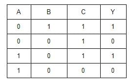
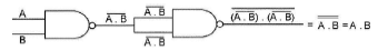
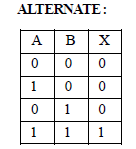
The following Figure shows a logic gate circuit with two inputs A and B and the output Y. The voltage waveforms of A, B and Y are given :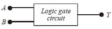
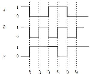 The logic gate is :
- a)NAND gate
- b)NOR gate
- c)OR gate
- d)AND gate
Correct answer is option 'A'. Can you explain this answer?
The following Figure shows a logic gate circuit with two inputs A and B and the output Y. The voltage waveforms of A, B and Y are given :
The logic gate is :
a)
NAND gate
b)
NOR gate
c)
OR gate
d)
AND gate
 | Aniket Chawla answered |
From the given waveforms, the truth table
is as follows.
is as follows.
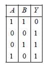
The above truth table is for NAND gate.
Therefore, the logic gate is NAND gate.
Therefore, the logic gate is NAND gate.
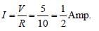
Two ideal diodes are connected to a battery as shown in the circuit. The current supplied by the battery is :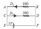
- a)0.75 A
- b)zero
- c)0.25 A
- d)0.5 A
Correct answer is option 'D'. Can you explain this answer?
Two ideal diodes are connected to a battery as shown in the circuit. The current supplied by the battery is :
a)
0.75 A
b)
zero
c)
0.25 A
d)
0.5 A
| | Aniket Chawla answered |
Here D1 is in forward bias and D2 is in
reverse bias so, D1 will conduct and D2 will
not conduct. Thus, no current will flow
through DC.
reverse bias so, D1 will conduct and D2 will
not conduct. Thus, no current will flow
through DC.


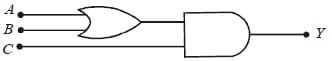
To get an output Y = 1 in the given circuit which of the following input will be correct:
[2012M]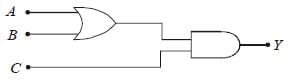
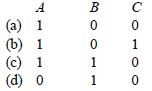
- a)a
- b)b
- c)c
- d)d
Correct answer is option 'B'. Can you explain this answer?
To get an output Y = 1 in the given circuit which of the following input will be correct:
[2012M]
[2012M]
a)
a
b)
b
c)
c
d)
d
| | Deepak Joshi answered |
When A = 1, B = 0, C = 1 then Y = 1
y1 = 1 + 0 = 1
y = y1C = 1.1 = 1
y1 = 1 + 0 = 1
y = y1C = 1.1 = 1
The figure shows a logic circuit with two inputs A and B and the output C. The voltage wave forms across A, B and C are as given. The logic circuit gate is : [2012]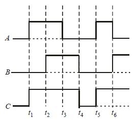
- a)OR gate
- b)NOR gate
- c)AND gate
- d)NAND gate
Correct answer is option 'A'. Can you explain this answer?
The figure shows a logic circuit with two inputs A and B and the output C. The voltage wave forms across A, B and C are as given. The logic circuit gate is : [2012]
a)
OR gate
b)
NOR gate
c)
AND gate
d)
NAND gate
| | Satyam answered |
A se the graph carefully
Chapter doubts & questions for Semiconductors - 30-Day Revision Course for NEET 2026 is part of NEET exam preparation. The chapters have been prepared according to the NEET exam syllabus. The Chapter doubts & questions, notes, tests & MCQs are made for NEET 2026 Exam. Find important definitions, questions, notes, meanings, examples, exercises, MCQs and online tests here.
Chapter doubts & questions of Semiconductors - 30-Day Revision Course for NEET in English & Hindi are available as part of NEET exam. Download more important topics, notes, lectures and mock test series for NEET Exam by signing up for free.
30-Day Revision Course for NEET85 videos|301 docs|171 tests |