


All Exams > Electrical Engineering (EE) > Topicwise Question Bank for Electrical Engineering > All Questions
All questions of Digital Electronics for Electrical Engineering (EE) Exam
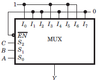
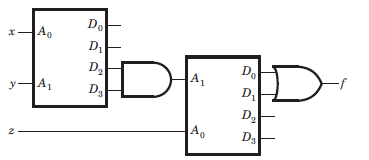
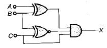
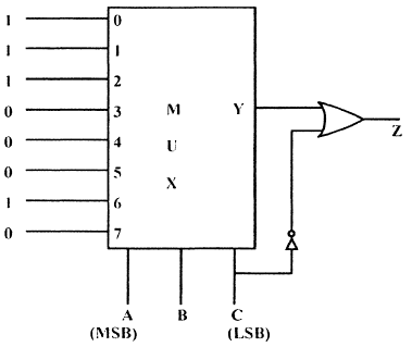
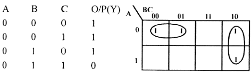
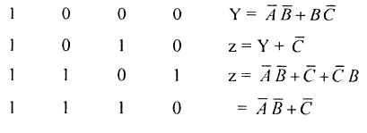
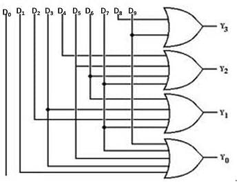
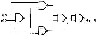
A MUX network is shown in fig.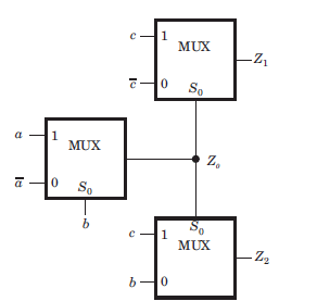 Que: This circuit act as a
- a)Full adder
- b)Half adder
- c)Full subtractor
- d)Half subtractor
Correct answer is option 'A'. Can you explain this answer?
A MUX network is shown in fig.
Que: This circuit act as a
a)
Full adder
b)
Half adder
c)
Full subtractor
d)
Half subtractor
 | Naroj Boda answered |
A 64 × 1 multiplexer has 64 inputs so if we use 2 × 1 multiplexers 32 are needed in the first stage for 64 inputs, the output of these 32 multiplexers are connected to inputs of 16 multiplexers in the second stage.
Similarly, in third stage, 8 (2 × 1) multiplexers are used, in fourth stage 4 are used and finally 2 (2 × 1) multiplexers in the fifth stage, 1 in the sixth stage.
Total 2 × 1 multiplexers needed are 32 + 16 + 8 + 4 + 2 + 1 = 63

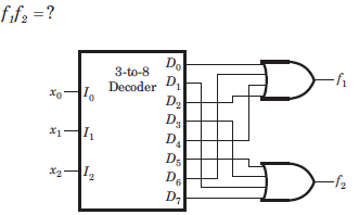
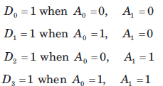
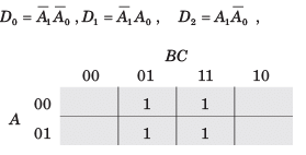
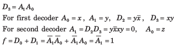
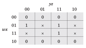
Can you explain the answer of this question below:A switching function of four variable, f (w, x y, z) is to equal the product of two other function f1 and f2, of the same variable f = f1f2 . The function f and f1 are as follows :
f = ∑m(4,7,15)
f = ∑m(0,1,2, 3, 4,7, 8,9,10,11,15)
Que: The number of full specified function, that will satisfy the given condition, is
- A:
32
- B:
16
- C:
4
- D:
1
The answer is a.
A switching function of four variable, f (w, x y, z) is to equal the product of two other function f1 and f2, of the same variable f = f1f2 . The function f and f1 are as follows :
f = ∑m(4,7,15)
f = ∑m(0,1,2, 3, 4,7, 8,9,10,11,15)
Que: The number of full specified function, that will satisfy the given condition, is
32
16
4
1
| | Ravi Singh answered |
f = ∑m(4,7,15)
f1 = ∑m(0,1,2, 3, 4,7, 8,9,10,11,15)
f2 = ∑m(4,7,15) + ∑dc(5, 6, 12, 13, 14)
There are 5 don't care condition. So 25 = 32 different functions f2
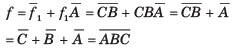
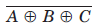
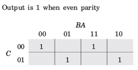
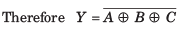
What are the essential prime implicants of following Boolean function x'z + y`z + xz'- a) x'z and y'z
- b) x'z & xz'
- c) y'z only
- d) xz' only.
Correct answer is option 'B'. Can you explain this answer?
What are the essential prime implicants of following Boolean function x'z + y`z + xz'
a)
x'z and y'z
b)
x'z & xz'
c)
y'z only
d)
xz' only.
 | Gate Gurus answered |
flx, y, z)= xlz + ylz + xzl These pairs are essential

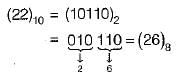
A decimal number (22)10 may be represented by the following ways: - a)(1 1 0 0 1)GRAY
- b) ( 1 0 1 1 0)2
- c)(26)8
- d)(16)18
Correct answer is option 'C'. Can you explain this answer?
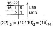
A decimal number (22)10 may be represented by the following ways:
a)
(1 1 0 0 1)GRAY
b)
( 1 0 1 1 0)2
c)
(26)8
d)
(16)18
| | Yash Patel answered |
The binary equivalent of (22)10 = (10110)2 as follows:
∴ (22)10 = (10110)2
- The GRAY code of (10110)2 is obtained as follows:
Thus, (10110)2 = (11101)gray
- The octal equivalent of (22)10 = (26)8 obtained as follows:
- The hexadecimal equivalent of (22)10 obtained as follows:


11001, 1001 and 111001 correspond to the 2’s complement representation of the following set of numbers- a)25, 9 and 57 respectively
- b)-6, -6 and -6 respectively
- c)-7, -7 and -7 respectively
- d)-25, -9 and -57 respectively
Correct answer is option 'C'. Can you explain this answer?
11001, 1001 and 111001 correspond to the 2’s complement representation of the following set of numbers
a)
25, 9 and 57 respectively
b)
-6, -6 and -6 respectively
c)
-7, -7 and -7 respectively
d)
-25, -9 and -57 respectively
 | Swara Dasgupta answered |
2's complement of 11001 = 00110 + 1 = 00111
00111 is 7 in decimal, so 11001 is 2's complement representation of -7.
2's complement of 1001 = 0110 + 1 = 0111
0111 is 7 in decimal, so 1001 is 2's complement representation of -7.
2's complement of 111001 = 000110 + 1 = 000111
000111 is 7 in decimal, so 111001 is 2's complement representation of -7.
The circuits of NOR based S-R latch classified as asynchronous sequential circuits, why?- a)Because of inverted outputs
- b)Because of triggering functionality
- c)Because of cross-coupled connection
- d)Because of inverted outputs & triggering functionality
Correct answer is option 'C'. Can you explain this answer?
The circuits of NOR based S-R latch classified as asynchronous sequential circuits, why?
a)
Because of inverted outputs
b)
Because of triggering functionality
c)
Because of cross-coupled connection
d)
Because of inverted outputs & triggering functionality
| | Pooja Patel answered |
The cross-coupled connections from the output of one gate to the input of the other gate constitute a feedback path. For this reason, the circuits of NOR based S-R latch classified as asynchronous sequential circuits. Moreover, they are referred to as asynchronous because they function in the absence of a clock pulse.
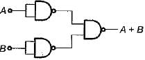
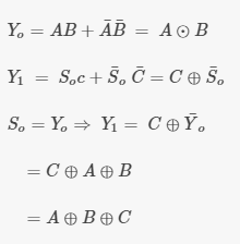
The reduced form of the Boolean expression of 
- a)A + B
- b)

- c)

- d)

Correct answer is option 'C'. Can you explain this answer?
The reduced form of the Boolean expression of
a)
A + B
b)
c)
d)
| | Arya Tiwari answered |
On multiplying the decimal number continuously by 2, the binary equivalent is obtained.
What is F's complement of (2BFD)16- a)E304
- b)D402
- c)D403
- d)C403
Correct answer is option 'B'. Can you explain this answer?
What is F's complement of (2BFD)16
a)
E304
b)
D402
c)
D403
d)
C403
| | Mahi Chavan answered |
F'S complement of 2BFD is FFF F - 2BFD = D402

Each product term of a group, w’.x.y’ and w.y, represents the ____________ in that group.- a)Input
- b)POS
- c)Sum-of-Minterms
- d)Sum of Maxterms
Correct answer is option 'C'. Can you explain this answer?
Each product term of a group, w’.x.y’ and w.y, represents the ____________ in that group.
a)
Input
b)
POS
c)
Sum-of-Minterms
d)
Sum of Maxterms
 | Husban Yousaf answered |
Because minters are called products of logic and of sets of variables
A signed integer has been stored in a byte using 2’s complement format. We wish to store the same integer in 16-bit word. We should copy the original byte to the less significant byte of the word and fill the more significant byte with- a)0
- b)1
- c)equal to the MSB of the original byte
- d)complement of the MSB of the original byte.
Correct answer is option 'C'. Can you explain this answer?
A signed integer has been stored in a byte using 2’s complement format. We wish to store the same integer in 16-bit word. We should copy the original byte to the less significant byte of the word and fill the more significant byte with
a)
0
b)
1
c)
equal to the MSB of the original byte
d)
complement of the MSB of the original byte.
 | Navya Sarkar answered |
See a example
A switching function of four variable, f (w, x y, z) is to equal the product of two other function f1and f2, of the same variable f = f1f2.The function f and f1are as follows : f =∑m(4,7,15) , f1 =∑m(0,1,2, 3, 4,7, 8,9,10,11,15)Que: The simplest function for f2 isa) xb)  c) yd)
  Correct answer is option 'A'. Can you explain this answer?
 | Aim It Academy answered |


Consider the following set of instruction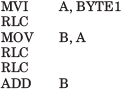 If BYTE1 = 07H, then content of A, after the execution of program will be
- a)46H
- b)70H
- c)38H
- d)68H
Correct answer is option 'A'. Can you explain this answer?
Consider the following set of instruction
If BYTE1 = 07H, then content of A, after the execution of program will be
a)
46H
b)
70H
c)
38H
d)
68H
| | Sanvi Kapoor answered |
This program multiply BYTE1 by 10. Hence content of A will be 46H.
07H = 0710 , 7 x 10 = 70, 7010 = 46H
Consider the following statements associated with logic gates:
1. Logic circuit of any complexity can be realised by using only the three basic gates namely AND, GR and NOT.
2. AND, OR and NOT .gates are called universal building blocks.
3. AND/OR/INVERT logic (AO! logic) can be converted to NAND logic or NOR logic.
4. A NAND gate can be used as an inverter by connecting all its input terminals except one, to logic 1 and applying the signal to be inverted to the remaining terminal.
Q. Which of the statements given above is/are correct?- a)1,3 and 4
- b)Only 3
- c)1 and 3
- d)1 and 4
Correct answer is option 'C'. Can you explain this answer?
Consider the following statements associated with logic gates:
1. Logic circuit of any complexity can be realised by using only the three basic gates namely AND, GR and NOT.
2. AND, OR and NOT .gates are called universal building blocks.
3. AND/OR/INVERT logic (AO! logic) can be converted to NAND logic or NOR logic.
4. A NAND gate can be used as an inverter by connecting all its input terminals except one, to logic 1 and applying the signal to be inverted to the remaining terminal.
Q. Which of the statements given above is/are correct?
a)
1,3 and 4
b)
Only 3
c)
1 and 3
d)
1 and 4
| | Dhruv Datta answered |
- Statement-1 is correct because any circuit can be realized using AND, OR and NOT gates.
- The two logic gates NAND and NOR can realize any logic circuit single-handedly. Hence, these two gates are called universal building blocks. AND, OR and NOT are called basic gates. Thus, statement-2 is not correct.
- Both NAND and NOR gates can perform all the three basic logic functions (AND, OR and NOT). Therefore, AND/OR/INVERT logic can be converted to NAND logic or NOR logic. Hence, statement-3 is correct.
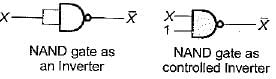
Statement-4 is not correct.
The output Y of a 2-bit comparator is logic 1 whenever the 2-bit input A is greater than the 2-bit input B. The number of combinations for which the output is logic 1, is- a)4
- b)6
- c)8
- d)10
Correct answer is option 'B'. Can you explain this answer?
The output Y of a 2-bit comparator is logic 1 whenever the 2-bit input A is greater than the 2-bit input B. The number of combinations for which the output is logic 1, is
a)
4
b)
6
c)
8
d)
10
 | Cstoppers Instructors answered |
The only possible combinations are
A = 01 and B = 0 0
A = 10 and B = 00, 01
A = 11 and B = 00, 01, 10
So there are only 6 combinations
Tips and Tricks:

where n = 2 bit
A = 01 and B = 0 0
A = 10 and B = 00, 01
A = 11 and B = 00, 01, 10
So there are only 6 combinations
Tips and Tricks:
where n = 2 bit
Consider the following statements associated with data representation by 1’s and 2‘s complements:
1. The 2’s complement system requires only one arithmetic operation.
2. The 1 ’s complement system requires two arithmetic operations.
3. The 1 's complement is often used in logical manipulations for inversion operation.
4. The 2 ’s complement is used only for arithmetic applications.Which of the statements given above are correct?- a)1 ,3 and 4
- b)1 , 2 , 3 and 4
- c)2, 3 and 4
- d)1,2 and 3
Correct answer is option 'A'. Can you explain this answer?
Consider the following statements associated with data representation by 1’s and 2‘s complements:
1. The 2’s complement system requires only one arithmetic operation.
2. The 1 ’s complement system requires two arithmetic operations.
3. The 1 's complement is often used in logical manipulations for inversion operation.
4. The 2 ’s complement is used only for arithmetic applications.
1. The 2’s complement system requires only one arithmetic operation.
2. The 1 ’s complement system requires two arithmetic operations.
3. The 1 's complement is often used in logical manipulations for inversion operation.
4. The 2 ’s complement is used only for arithmetic applications.
Which of the statements given above are correct?
a)
1 ,3 and 4
b)
1 , 2 , 3 and 4
c)
2, 3 and 4
d)
1,2 and 3
| | Sarita Yadav answered |
1, 3, and 4
Explanation:
1. The 2's complement system requires only one arithmetic operation: This statement is correct. In the 2's complement system, both addition and subtraction can be performed with the same operation (addition). To subtract, we simply add the 2's complement of the number to be subtracted.
2. The 1's complement system requires two arithmetic operations: This statement is incorrect. The 1's complement system also requires only one arithmetic operation (addition) for both addition and subtraction. However, in this system, an end-around carry might be needed for the final result.
3. The 1's complement is often used in logical manipulations for inversion operation: This statement is correct. The 1's complement can be used to invert the bits of a binary number (changing 0s to 1s and vice versa). This operation is useful for logical operations like bitwise NOT.
4. The 2's complement is used only for arithmetic applications: This statement is correct. The 2's complement representation is primarily used for arithmetic operations, such as addition and subtraction, as it simplifies the operations and eliminates the need for separate circuits for these operations.
Consider the following program of 8085 assembly language: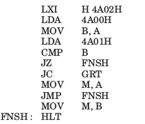 Que: The memory requirement for this program is
- a)20 Byte
- b)21 Byte
- c)23 Byte
- d)18 Byte
Correct answer is option 'C'. Can you explain this answer?
Consider the following program of 8085 assembly language:
Que: The memory requirement for this program is
a)
20 Byte
b)
21 Byte
c)
23 Byte
d)
18 Byte
| | Kabir Verma answered |
Operand R, M or implied : 1–Byte instruction
Operand 8–bit : 2–Byte instruction
Operand 16–bit : 3–Byte instruction
Operand 8–bit : 2–Byte instruction
Operand 16–bit : 3–Byte instruction
3–Byte instruction are: LXI, LDA, JZ, JC, JMP
P–Byte instruction are : MOV, CMP, HLT
P–Byte instruction are : MOV, CMP, HLT
Hence memory = 3 x 6 + 1 x 5 = 23 bytes
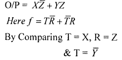
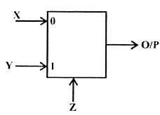
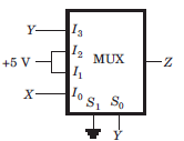
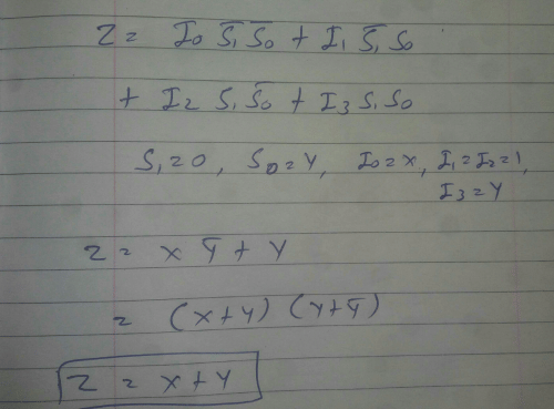
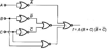
Consider a multiplexer with X &Y as data inputs and z as a control pin. If Z = 0, selects input X and Z = I , selects input Y what are the connections required to realize the 2 - variable Boolean functions f T R
R- a) 1 to X' and T' to Y
- b) T to X, T' to Y, R to Z
- c) 1 to X, 0 to Y, T to Z
- d) T to X, T' to Y, R to X
Correct answer is option 'B'. Can you explain this answer?
Consider a multiplexer with X &Y as data inputs and z as a control pin. If Z = 0, selects input X and Z = I , selects input Y what are the connections required to realize the 2 - variable Boolean functions f T R
Ra)
1 to X' and T' to Y
b)
T to X, T' to Y, R to Z
c)
1 to X, 0 to Y, T to Z
d)
T to X, T' to Y, R to X
| | Vedika Singh answered |
The initial state of MOD — 16, down counter is 0110. What state will be it be after 37 clock pulses??- a) Indeterminate
- b) 0110
- c) 0101
- d) 0001
Correct answer is option 'D'. Can you explain this answer?
The initial state of MOD — 16, down counter is 0110. What state will be it be after 37 clock pulses??
a)
Indeterminate
b)
0110
c)
0101
d)
0001
 | Anirban Khanna answered |
I.
After every 16 clock pulse counter reach to initial state.
After 32 clock pulses counter will be at 0110
after 33 clock pulse, 0101
After 34 clock pulse, 0100
After 35 clock pulse, 0011
After 36 clock pulse, 0010
After 37 clock pulse, 0001.
II
After Every 16 clock pulses counter will be at initial state, 0110
37 mod 16 = 5.
As it is a down counter, it will be 5 states down from 0110 = 0110 - 0101= 0001.
How many OR gates are required for a Decimal-to-bcd encoder?- a)2
- b)10
- c)3
- d)4
Correct answer is option 'D'. Can you explain this answer?
How many OR gates are required for a Decimal-to-bcd encoder?
a)
2
b)
10
c)
3
d)
4
| | Pooja Patel answered |
An encoder is a combinational circuit encoding the information of 2n input lines to n output lines, thus producing the binary equivalent of the input.
This is clear from the diagram that it requires 4 OR gates:
This is clear from the diagram that it requires 4 OR gates:
Conversion of excess-3 code to BCD code can be achieved by using- a)4 x 16 decoder
- b)4 bit Full adder
- c)4 x 16 De-MUX
- d)4 bit Half adder
Correct answer is option 'C'. Can you explain this answer?
Conversion of excess-3 code to BCD code can be achieved by using
a)
4 x 16 decoder
b)
4 bit Full adder
c)
4 x 16 De-MUX
d)
4 bit Half adder
| | Sinjini Mehta answered |
The number of AND gates required will be equal to the number of outputs in a demultiplexer.


An 8085 Microprocessor based system uses a 4 k x 8 bit RAM whose starting address is AAOOH. The address of last byte in this RAM is- a) OFFFH
- b) 1000 H
- c) B9 FFH
- d)BAOOH
Correct answer is option 'C'. Can you explain this answer?
An 8085 Microprocessor based system uses a 4 k x 8 bit RAM whose starting address is AAOOH. The address of last byte in this RAM is
a)
OFFFH
b)
1000 H
c)
B9 FFH
d)
BAOOH
| | Sanya Agarwal answered |
4K x 8 = 212 x 8 bit it has 12 bits So address of last - byte will be AA 00 + 0 FFF = B9FF
112 4-bit 2's complement no's 1011 and 0110 are added, then result expressed in 2's complementnotation is- a) 0001
- b) 0010
- c) 1101
- d) Can not be expressed in 4 bit 2's complement
Correct answer is option 'A'. Can you explain this answer?
112 4-bit 2's complement no's 1011 and 0110 are added, then result expressed in 2's complementnotation is
a)
0001
b)
0010
c)
1101
d)
Can not be expressed in 4 bit 2's complement
 | Shivani Yadav answered |
Solution:
Conversion of 2s complement numbers:
• 1011 → -5
• 0110 → 6
Addition of two 4-bit 2s complement numbers:
• -5 + 6 = 1
Since the result is positive, it can be represented in 4-bit 2s complement notation as:
• 0001
Therefore, the correct answer is option 'A' (0001).
Conversion of 2s complement numbers:
• 1011 → -5
• 0110 → 6
Addition of two 4-bit 2s complement numbers:
• -5 + 6 = 1
Since the result is positive, it can be represented in 4-bit 2s complement notation as:
• 0001
Therefore, the correct answer is option 'A' (0001).
What is the function of an enable input on a multiplexer chip?- a)To apply Vcc
- b)To connect ground
- c)To active the entire chip
- d)To active one half of the chip
Correct answer is option 'C'. Can you explain this answer?
What is the function of an enable input on a multiplexer chip?
a)
To apply Vcc
b)
To connect ground
c)
To active the entire chip
d)
To active one half of the chip
| | Siddharth Khanna answered |
The function of an enable input on a multiplexer chip is to activate or deactivate the entire chip. When the enable input is high (or active), the multiplexer chip is enabled and can perform its intended function. On the other hand, when the enable input is low (or inactive), the multiplexer chip is disabled and its outputs are in a high-impedance state.
When the enable input is active, the multiplexer chip acts as a data selector, allowing one of multiple inputs to be selected and routed to the output. The selection of the input is determined by the control inputs of the chip.
Below is a detailed explanation of the function of the enable input on a multiplexer chip:
1. Multiplexer Basics:
- A multiplexer, also known as a data selector, is a digital circuit that selects one of many inputs and routes it to a single output.
- It is commonly represented by the symbol ⊕ or MUX.
2. Enable Input:
- The enable input on a multiplexer chip is denoted as EN or E, and it controls the activation of the chip.
- The enable input is typically an active-high input, meaning that when it is high (logic 1), the chip is enabled.
3. Chip Activation:
- When the enable input is active (high), the multiplexer chip is enabled and can perform its function.
- The chip becomes operational, and its outputs are determined by the control inputs and the selected input.
- The selected input is determined by the control inputs, such as address lines or select inputs.
4. Chip Deactivation:
- When the enable input is inactive (low), the multiplexer chip is disabled.
- The chip enters a high-impedance state, which means that its outputs are effectively disconnected and do not drive any signal.
- This high-impedance state prevents any interference or conflicts with other circuitry that may be connected to the outputs of the disabled chip.
5. Usefulness of Enable Input:
- The enable input is useful in applications where the activation or deactivation of the multiplexer chip needs to be controlled.
- It allows for greater flexibility in circuit design by providing the ability to enable or disable the chip as needed.
In summary, the enable input on a multiplexer chip is responsible for activating or deactivating the entire chip. When the enable input is high, the chip is enabled and can perform its function of selecting and routing one of multiple inputs to the output. When the enable input is low, the chip is disabled, and its outputs are in a high-impedance state.
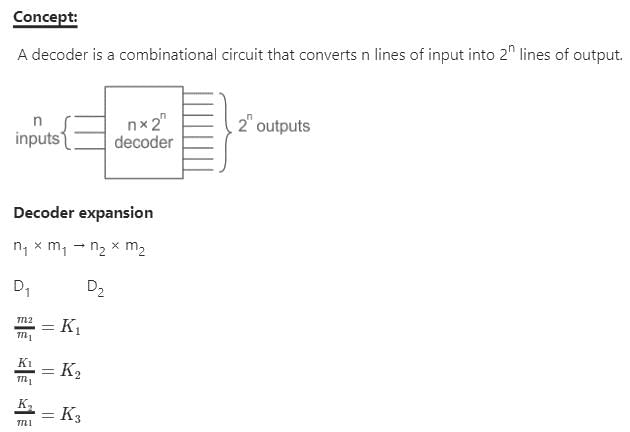
It is possible for an enable or strobe input to undergo an expansion of two or more MUX ICs to the digital multiplexer with the proficiency of large number of _______- a)Inputs
- b)Outputs
- c)Selection lines
- d)Enable lines
Correct answer is option 'A'. Can you explain this answer?
It is possible for an enable or strobe input to undergo an expansion of two or more MUX ICs to the digital multiplexer with the proficiency of large number of _______
a)
Inputs
b)
Outputs
c)
Selection lines
d)
Enable lines
| | Ashutosh Majumdar answered |
Answer:
To understand the answer to this question, let's first discuss the basic concept of a digital multiplexer.
A digital multiplexer, also known as a data selector, is a combinational circuit that selects one of many input signals and routes it to a single output line based on the control inputs. It is widely used in various electronic applications, such as data transmission, signal routing, and digital communication systems.
A multiplexer can have multiple inputs, outputs, and selection lines. The selection lines determine which input signal gets routed to the output line. The number of selection lines in a multiplexer is determined by the number of input lines and is given by the equation:
n = log2(N)
Where n is the number of selection lines and N is the number of input lines. For example, if we have 4 input lines, we would need 2 selection lines (n = log2(4) = 2).
In the given question, it is mentioned that an enable or strobe input undergoes an expansion of two or more multiplexer ICs. This means that multiple multiplexer ICs are cascaded together to form a larger multiplexer.
When multiple multiplexer ICs are cascaded, the enable or strobe input of each IC is connected in parallel. This allows the enable or strobe input to control the operation of all the cascaded ICs simultaneously.
By expanding the multiplexer using multiple ICs, we can increase the number of inputs that can be selected. Each IC will have a certain number of inputs, outputs, and selection lines. By cascading multiple ICs together, we can effectively increase the number of inputs of the multiplexer.
However, it is important to note that the number of outputs and selection lines remains the same, as these are determined by the individual ICs. Only the number of inputs can be increased by cascading multiple ICs.
Therefore, the correct answer to the given question is option 'A' - Inputs.
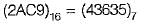
If (2AC9)16 = (Z)7, then the value of Z is- a)43635
- b)58477
- c)42587
- d)38999
Correct answer is option 'A'. Can you explain this answer?
If (2AC9)16 = (Z)7, then the value of Z is
a)
43635
b)
58477
c)
42587
d)
38999
| | Sanskriti Bajaj answered |
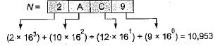
Thus, (2AC9)16 - (10,953)10
Now, the decimal number is converted into the number of base 7 as follows:
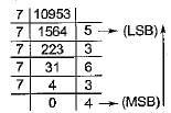
Thus
If half adders and full adders are implements using gates, then for the addition of two 17 bit numbers (using minimum gates) the number of half adders and full adders required will be- a)0, 17
- b)16, 1
- c)1, 16
- d)8, 8
Correct answer is option 'C'. Can you explain this answer?
If half adders and full adders are implements using gates, then for the addition of two 17 bit numbers (using minimum gates) the number of half adders and full adders required will be
a)
0, 17
b)
16, 1
c)
1, 16
d)
8, 8
 | Imtiaz Ahmad answered |
Take 2 numbers for 17 bits, for the first 2 bits of each number we need one-half adder and for rest(16 bit of each number) we will have one carry of previous sum and two bits of each number so we need one full adder for each rest of bits, that is, 16 full adder.
The number of two input NAND gate required to implement an OR gate and an EX-NOR gate are respectively- a)2 and 5
- b)3 and 4
- c)3 and 5
- d)2 and 4
Correct answer is option 'C'. Can you explain this answer?
The number of two input NAND gate required to implement an OR gate and an EX-NOR gate are respectively
a)
2 and 5
b)
3 and 4
c)
3 and 5
d)
2 and 4
| | Prasad Saini answered |
OR gate using NAND gate:
EX-NOR gate using NAND gate:
Thus, we require 3 NAND gates for an OR gate while 5 NAND gates for an EX-NOR gate.
EX-NOR gate using NAND gate:
Thus, we require 3 NAND gates for an OR gate while 5 NAND gates for an EX-NOR gate.
Consider the following statements associated with the use of various adder circuits:
1. A ripple carry adder is a parallel adder in which the carry-out of each full-adder is the carry-in to the next most significant adder.
2. Serial adders are used where speed is more important than circuit minimization.
3. The look-ahead carry adder speeds up the process by eliminating the ripple carry.
4. Serial adders are faster than parallel addersWhich of the statements given above are correct?- a)1,2 and 4
- b)2 and 4 only
- c)1 and 3 only
- d)2, 3 and 4
Correct answer is option 'C'. Can you explain this answer?
Consider the following statements associated with the use of various adder circuits:
1. A ripple carry adder is a parallel adder in which the carry-out of each full-adder is the carry-in to the next most significant adder.
2. Serial adders are used where speed is more important than circuit minimization.
3. The look-ahead carry adder speeds up the process by eliminating the ripple carry.
4. Serial adders are faster than parallel adders
Which of the statements given above are correct?
a)
1,2 and 4
b)
2 and 4 only
c)
1 and 3 only
d)
2, 3 and 4
| | Sanchita Choudhary answered |
- Serial adders are used where circuit minimization is more important than speed because they require one clock pulse for each pair of bits added and hence slower than parallel adders. Thus, statements 2 and 4 are not correct.
- Statements 1 and 3 are correct.
Consider the following statements:
1. Sequential circuits are always faster than combination circuits.
2. In an asynchronous circuit there is no problem of stability.
3. The logic circuits whose outputs at any instant of time depend only on the input signals present at that time are known as combinational circuits.
4. In a combinational circuit, for a change in the input, the output appears immediately.
5. In a sequential circuits, the output signals are fed back to the input side.Which of the statement given above are correct? - a)2, 3 and 4
- b)1. and 5 only
- c)3 and 5 only
- d)1,2 and 4
Correct answer is option 'C'. Can you explain this answer?
Consider the following statements:
1. Sequential circuits are always faster than combination circuits.
2. In an asynchronous circuit there is no problem of stability.
3. The logic circuits whose outputs at any instant of time depend only on the input signals present at that time are known as combinational circuits.
4. In a combinational circuit, for a change in the input, the output appears immediately.
5. In a sequential circuits, the output signals are fed back to the input side.
Which of the statement given above are correct?
a)
2, 3 and 4
b)
1. and 5 only
c)
3 and 5 only
d)
1,2 and 4
| | Muskaan Nair answered |
• Combinational circuits are often faster than sequential circuits since the combinations circuits do not require memory whereas the sequential circuits need memory devices to perform their operations in sequence. Hence statement - 1 is not correct.
• in an asynchronous circuit, events are allowed to occur without any synchronisation In such a case, the system become: unstable which results in difficulties. Hence statement-2 is not correct.
• Statement-3 is correct which is the definitioi of a combinational circuit.
• in a combinational circuit, for a change if the input, the output appears immediately except for the propagation delay througt circuit gates. Thus, statement-4 is no correct.
• In a sequential circuit, an output signal is e function of the present input signals and e sequence of the past input signals i.e. the past output signals since the output signals are fed back to the input side. Hence, statement-5 is correct.
Thus, statements 3 and 5 are only correct.
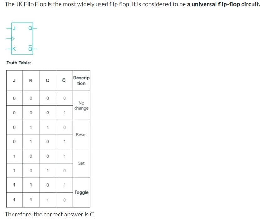
What J-K input condition will always set ‘Q+ upon the occurrence of the active clock transition ?- a)J = 1, K = 0
- b)J = 1 , K = 1
- c)J = 0 , K = 1
- d)J = 0, K = 0
Correct answer is option 'A'. Can you explain this answer?
What J-K input condition will always set ‘Q+ upon the occurrence of the active clock transition ?
a)
J = 1, K = 0
b)
J = 1 , K = 1
c)
J = 0 , K = 1
d)
J = 0, K = 0
| | Shivam Das answered |
Truth table for J-K flip-flop is shown below.
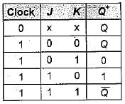
When J = 1 and K = 0, output (Q+) is always set upon the occurrence of the active clock transition.
When J = 1 and K = 0, output (Q+) is always set upon the occurrence of the active clock transition.
Synchronous counter is a type of ____________- a)SSI counters
- b)LSI counters
- c)MSI counters
- d)VLSI counters
Correct answer is option 'C'. Can you explain this answer?
Synchronous counter is a type of ____________
a)
SSI counters
b)
LSI counters
c)
MSI counters
d)
VLSI counters
| | Pooja Patel answered |
Synchronous Counter is a Medium Scale Integrated (MSI). In Synchronous Counters, the clock pulse is supplied to all the flip-flops simultaneously.
In the truth table of an N-input OR gate, in the column for the output of the gate,- a)the number of zeros is equal to N.
- b)the number of zeros is always 1.
- c)the output is zero if any one of the input is zero
- d)the number of times a zero occurs is a complex function of N.
Correct answer is option 'B'. Can you explain this answer?
In the truth table of an N-input OR gate, in the column for the output of the gate,
a)
the number of zeros is equal to N.
b)
the number of zeros is always 1.
c)
the output is zero if any one of the input is zero
d)
the number of times a zero occurs is a complex function of N.
| | Vaibhav Joshi answered |
A two input OR gate truth table is shown below:
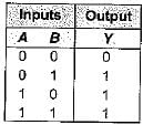
From the truth table of OR gate it is clear tha output is 0’s only when all the inputs are 0’s otherwise for all other input combination outpu is always 1's. Hence, in the column for the outpu of the OR gate, the number of zeros is always 1's.
From the truth table of OR gate it is clear tha output is 0’s only when all the inputs are 0’s otherwise for all other input combination outpu is always 1's. Hence, in the column for the outpu of the OR gate, the number of zeros is always 1's.
Find the number of 2 × 1 MUX (multiplexers) required to implement 16 × 1 MUX.- a)15
- b)20
- c)5
- d)9
Correct answer is option 'A'. Can you explain this answer?
Find the number of 2 × 1 MUX (multiplexers) required to implement 16 × 1 MUX.
a)
15
b)
20
c)
5
d)
9
| | Mayank Sengupta answered |
It seems like you were cut off mid-sentence. Could you please provide more context or complete your question?
Which is the major functioning responsibility of the multiplexing combinational circuit?- a)Decoding the binary information
- b)Generation of all minterms in an output function with OR-gate
- c)Generation of selected path between multiple sources and a single destination
- d)Encoding of binary information
Correct answer is option 'C'. Can you explain this answer?
Which is the major functioning responsibility of the multiplexing combinational circuit?
a)
Decoding the binary information
b)
Generation of all minterms in an output function with OR-gate
c)
Generation of selected path between multiple sources and a single destination
d)
Encoding of binary information
 | Isha Bajaj answered |
The major functioning responsibility of a multiplexing combinational circuit is the generation of a selected path between multiple sources and a single destination. Let's break down this answer in detail:
1. What is a multiplexing combinational circuit?
A multiplexing combinational circuit is a digital circuit that allows multiple input signals to be transmitted over a single transmission line or channel. It uses a combination of logic gates to select and route the desired input signal to the output.
2. Understanding the options:
a) Decoding the binary information:
Decoding refers to the process of converting a binary code into a more meaningful form. While decoding can be a part of the multiplexing process, it is not the major functioning responsibility of the circuit.
b) Generation of all minterms in an output function with OR-gate:
A minterm is a product term in Boolean algebra that represents a specific combination of input variables. While generating minterms can be a part of the multiplexing process, it is not the major functioning responsibility of the circuit.
c) Generation of selected path between multiple sources and a single destination:
This is the correct answer. The main purpose of a multiplexing combinational circuit is to select and route the desired input signal to a single output destination. It allows multiple sources to share a common transmission line or channel, enabling efficient communication.
d) Encoding of binary information:
Encoding refers to the process of converting meaningful data into a coded form. While encoding can be a part of the multiplexing process, it is not the major functioning responsibility of the circuit.
3. Importance of selecting a path:
In many applications, especially in communication systems, there is a need to transmit multiple signals over limited resources. Multiplexing allows efficient utilization of these resources by selecting and routing the desired signals to their respective destinations. By choosing the appropriate path, the multiplexing combinational circuit ensures that the desired signal reaches the destination without interference or loss.
4. How the circuit works:
The multiplexing combinational circuit uses logic gates, such as AND gates and OR gates, to select the desired input signal based on control signals. These control signals determine which input signal is routed to the output. By manipulating the control signals, different input signals can be selected and transmitted at different times, effectively sharing the transmission line or channel.
In conclusion, the major functioning responsibility of a multiplexing combinational circuit is to generate a selected path between multiple sources and a single destination. It allows efficient utilization of resources and enables the transmission of multiple signals over a common transmission line or channel.
The minimum number of NOR gates requires to implement the expression
f(A, B, C) = πM(0, 1, 2, 3, 4, 7) is- a)5
- b)4
- c)7
- d)6
Correct answer is option 'D'. Can you explain this answer?
The minimum number of NOR gates requires to implement the expression
f(A, B, C) = πM(0, 1, 2, 3, 4, 7) is
f(A, B, C) = πM(0, 1, 2, 3, 4, 7) is
a)
5
b)
4
c)
7
d)
6
| | Shivam Das answered |
Given expressio n is f = πM( 0, 1, 2, 3, 4, 7)
The K-map for this expression is shown below.
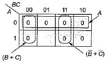
The minimized expression in POS form is
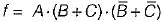
The minimized expression 'f' can be implemented using two input NOR gate as shown below.
Thus, we require six NOR gates.
The K-map for this expression is shown below.
The minimized expression in POS form is
The minimized expression 'f' can be implemented using two input NOR gate as shown below.
Thus, we require six NOR gates.


The flag bits in an ALU is defined as ___________- a)The total number of registers
- b)The status bit conditions
- c)The total number of control lines
- d)All of the Mentioned
Correct answer is option 'B'. Can you explain this answer?
The flag bits in an ALU is defined as ___________
a)
The total number of registers
b)
The status bit conditions
c)
The total number of control lines
d)
All of the Mentioned
| | Sravya Khanna answered |
Flag bits in an ALU
The flag bits in an Arithmetic Logic Unit (ALU) are defined as the status bit conditions. These flag bits are used to indicate the results of arithmetic and logical operations performed by the ALU. They provide information about the outcome of an operation, such as whether a result is zero, negative, or positive.
Understanding flag bits
Flag bits are important for program control and decision making. They are used by the control unit to determine the next course of action based on the results of the ALU operation. The flag bits are typically stored in a register or a set of registers within the ALU.
Types of flag bits
There are several types of flag bits that are commonly found in ALUs:
1. Zero (Z) flag: This flag is set when the result of an operation is zero. It indicates that the two operands of the operation are equal.
2. Carry (C) flag: This flag is set when an arithmetic operation generates a carry or borrow. It is used in multi-digit addition and subtraction operations.
3. Sign (S) flag: This flag indicates the sign of the result. It is set when the result is negative.
4. Overflow (V) flag: This flag is set when an arithmetic operation results in an overflow, which occurs when the result is too large to be represented using the available number of bits.
Importance of flag bits
Flag bits are crucial for program execution as they allow the control unit to make decisions based on the outcome of ALU operations. For example, the zero flag may be used to check if a value is equal to zero, while the carry flag may be used for implementing arithmetic operations on larger numbers.
Conclusion
In conclusion, the flag bits in an ALU are defined as the status bit conditions. They provide information about the outcome of arithmetic and logical operations performed by the ALU. The flag bits are essential for program control and decision making, allowing the control unit to determine the next course of action based on the results of the ALU operation.
Chapter doubts & questions for Digital Electronics - Topicwise Question Bank for Electrical Engineering 2026 is part of Electrical Engineering (EE) exam preparation. The chapters have been prepared according to the Electrical Engineering (EE) exam syllabus. The Chapter doubts & questions, notes, tests & MCQs are made for Electrical Engineering (EE) 2026 Exam. Find important definitions, questions, notes, meanings, examples, exercises, MCQs and online tests here.
Chapter doubts & questions of Digital Electronics - Topicwise Question Bank for Electrical Engineering in English & Hindi are available as part of Electrical Engineering (EE) exam. Download more important topics, notes, lectures and mock test series for Electrical Engineering (EE) Exam by signing up for free.