


All Exams > Electrical Engineering (EE) > Electrical Engineering SSC JE (Technical) > All Questions
All questions of Basic Electronics for Electrical Engineering (EE) Exam
Nuclues is made of–- a)Electrons and protons
- b)Protons and neutrons
- c)Photons and neutrons
- d)Photons and electrons
Correct answer is option 'B'. Can you explain this answer?
Nuclues is made of–
a)
Electrons and protons
b)
Protons and neutrons
c)
Photons and neutrons
d)
Photons and electrons
 | Bijoy Kapoor answered |
Atomic particles. Protons and neutrons are heavier than electrons and reside in the nucleus at the center of the atom. Electrons are extremely lightweight and exist in a cloud orbiting the nucleus. OPTION B IS CORRECT.

The transistor configuration which provides highest output impedance is :- a)Common Base
- b)Common Emitter
- c)Common Collector
- d)None of the above
Correct answer is option 'A'. Can you explain this answer?
The transistor configuration which provides highest output impedance is :
a)
Common Base
b)
Common Emitter
c)
Common Collector
d)
None of the above
| | Harshad Singh answered |
Explanation:
The output impedance of a transistor circuit is defined as the ratio of the change in output voltage to the change in output current. It is an important parameter to consider while designing amplifier circuits as it determines the load that can be connected to the circuit without affecting its performance.
The three basic transistor configurations are common base (CB), common emitter (CE), and common collector (CC). Each configuration has its own characteristics and advantages, but when it comes to output impedance, the common base configuration provides the highest output impedance.
Reasons why common base configuration provides highest output impedance:
1. Current gain is low: In common base configuration, the input signal is applied to the emitter and the output is taken from the collector. The base is common to both input and output circuits. The current gain in this configuration is low due to the fact that the base current is small compared to the emitter current. As a result, the output impedance is high.
2. Voltage gain is high: In common base configuration, the voltage gain is high due to the fact that the input impedance is low and the output impedance is high. This makes it suitable for impedance matching applications.
3. Low power output: In common base configuration, the power output is low due to the fact that the collector current is small compared to the emitter current. This makes it suitable for high-frequency applications where low power is required.
Conclusion:
In conclusion, the common base configuration provides the highest output impedance due to its low current gain, high voltage gain, and low power output. This makes it suitable for applications where high input impedance and low output impedance are required.

The emitter of a transistor is doped the heaviest because of it :
- A:
dissipates maximum power
- B:
is supplier of charge carriers
- C:
receives the input
- D:
should have low resistance
The answer is b.
dissipates maximum power
is supplier of charge carriers
receives the input
should have low resistance
 | Kaavya Sengupta answered |
The role of the emitter region is to emit or inject current carriers into the base region, which then moves to the collector region of the transistor, where the transistor outputs the current signal.
In a bipolar junction transistor, majority charge carriers flow from the emitter to the collector and then out from the collector. In other words, when electrons flow from emitter to collector, the current flows from collector to emitter for NPN transistor and vice versa in PNP transistor.
The reason the emitter is the most heavily doped region is because it serves to inject a large amount of charge carriers into the base, which then travels into the collector, so that switching or amplification can occur.
For a NPN bipolar transistor, what is the main stream of current in the base region?- a)Drift of holes.
- b)Diffusion of holes
- c)Drift of electrons
- d)Diffusion of electrons
Correct answer is 'B'. Can you explain this answer?
For a NPN bipolar transistor, what is the main stream of current in the base region?
a)
Drift of holes.
b)
Diffusion of holes
c)
Drift of electrons
d)
Diffusion of electrons
 | Anirban Khanna answered |
Diffusion current is a current in a semiconductor caused by the diffusion of charge carriers (holes and/or electrons). ... Diffusion current can be in the same or opposite direction of a drift current.
The phenomenon known as "Early Effect" in a bipolar transistor refers to a reduction of theeffective base-width caused by- a)electron-hole recombination at the base
- b)the reverse biasing of the base -collector junction
- c)the forward biasing of emitter -base junction
- d)the early removal of stored base charge during saturation-to-cutoff switcing
Correct answer is option 'B'. Can you explain this answer?
The phenomenon known as "Early Effect" in a bipolar transistor refers to a reduction of theeffective base-width caused by
a)
electron-hole recombination at the base
b)
the reverse biasing of the base -collector junction
c)
the forward biasing of emitter -base junction
d)
the early removal of stored base charge during saturation-to-cutoff switcing
| | Shashank Shukla answered |
0 voltage
A silicon transistor with VBE sat = 0.8 V, b dc = 100 and VCE sat = 0.2 V is used in the circuit shown in given figure What is the minimum value of RC for which transistor is in saturation ?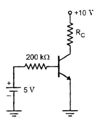
- a)4286W
- b)4667W
- c)500W
- d)1000W
Correct answer is 'B'. Can you explain this answer?
A silicon transistor with VBE sat = 0.8 V, b dc = 100 and VCE sat = 0.2 V is used in the circuit shown in given figure What is the minimum value of RC for which transistor is in saturation ?
a)
4286W
b)
4667W
c)
500W
d)
1000W
 | Engineers Adda answered |
Step 1
Apply kvl in 1 loop
5 - IbRb - 0.8 =0
5 - Ib*(200*1000ohm) - 0.8 =0
Base current (Ib)=(5-0.8)/(200*1000ohm)
=(4.2)/(200*1000)
=(2.1)/(100000)
5 - IbRb - 0.8 =0
5 - Ib*(200*1000ohm) - 0.8 =0
Base current (Ib)=(5-0.8)/(200*1000ohm)
=(4.2)/(200*1000)
=(2.1)/(100000)
2nd step
we know, collector current (Ic)= beta times of base current
so, Ic=(100*2.1)/(100000)=0.0021
so, Ic=(100*2.1)/(100000)=0.0021
3 step:-
Apply kvl in 2 loop
10 - 0.0021*Rc - 0.2 =0
minimum value of Rc is
Rc=(9.8)/(0.0021)
=4666.66ohm
=4667 ohm
10 - 0.0021*Rc - 0.2 =0
minimum value of Rc is
Rc=(9.8)/(0.0021)
=4666.66ohm
=4667 ohm
Two P-N junction diodes are connected back to back to make a transistor. Which one of the following is correct?- a)the current gain of such a transistor will be high.
- b)the current gain of such a transistor will be moderate
- c)it cannot be used a s a transistor due to large base width.
- d)it can be used only for PNP transistor
Correct answer is option 'C'. Can you explain this answer?
Two P-N junction diodes are connected back to back to make a transistor. Which one of the following is correct?
a)
the current gain of such a transistor will be high.
b)
the current gain of such a transistor will be moderate
c)
it cannot be used a s a transistor due to large base width.
d)
it can be used only for PNP transistor
| | Aisha Gupta answered |
This doesn't work because base region is wide and are equally doped, whereas in actual transistor base is very thin and lightly doped. In two discrete diodes connected back-to-back, has 4 doped regions instead of 3. Hence, two diodes connected back-to-back can never be used as a transistor.
Voltage power supplies use a high resistance across the output of the supply. That resistance is called- a) high Voltage resistors.
- b) potentiometers.
- c) bleeder resistors.
- d) holding resistors.
Correct answer is option 'C'. Can you explain this answer?
Voltage power supplies use a high resistance across the output of the supply. That resistance is called
a)
high Voltage resistors.
b)
potentiometers.
c)
bleeder resistors.
d)
holding resistors.
| | Prasad Saini answered |
Bleeder resistors are standard high value resistors which are used to discharge the capacitor in filter circuit. The discharging of the capacitors is really important because even if the power supply is OFF, a charged capacitor can give a shock to anybody.
For the BJT circuit shown, assume that the b of the transistor is very large and VBE = 0.7 V. The mode of operation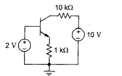
- a)cutoff
- b)saturation
- c)normal active
- d)reverse active
Correct answer is option 'B'. Can you explain this answer?
For the BJT circuit shown, assume that the b of the transistor is very large and VBE = 0.7 V. The mode of operation
a)
cutoff
b)
saturation
c)
normal active
d)
reverse active
 | Baishali Bajaj answered |
Considering collector to base voltage (𝑉𝐶𝐵) is 0.2V
Emitter base junction forward biased Collector base junction Reverse biased Input junction F.B and output junction R.B
For the circuit shown in figure given below, assume b = hFE = 100. The transistor is in =100.The transistor is in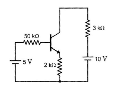
- a)active region and VCE = 5 V.
- b)saturation region
- c)active region and VCE = 1.42 V.
- d)cut off region.
Correct answer is option 'B'. Can you explain this answer?
For the circuit shown in figure given below, assume b = hFE = 100. The transistor is in =100.The transistor is in
a)
active region and VCE = 5 V.
b)
saturation region
c)
active region and VCE = 1.42 V.
d)
cut off region.
 | Vidya K S answered |
Cut off region
when a transistor is used in switching mode then what is the turn on time ?- a)sum of delay time and rise time
- b)Sum of rise time and storage time
- c)Sum of delay time and storage time
- d)Sum of rise time and fall time
Correct answer is option 'A'. Can you explain this answer?
when a transistor is used in switching mode then what is the turn on time ?
a)
sum of delay time and rise time
b)
Sum of rise time and storage time
c)
Sum of delay time and storage time
d)
Sum of rise time and fall time
| | Rajeev Sharma answered |
Turn-on time of the transistor is the time taken by the transistor from the instant the pulse is applied to the instant the transistor switches into the ON state and is the sum of the delay time (td) and rise time (tr).
T(on) = tr + td
To find out the turn-on time of the transistor, the delay time and rise time have to be calculated.
P-type semiconductors are–- a)Positively charged
- b)Electrically neutral
- c)Obtained when phosphorus is added as impurity to silicon or germanium
- d)Obtained when arsenic is added as impurity to germanium or silicon
Correct answer is option 'B'. Can you explain this answer?
P-type semiconductors are–
a)
Positively charged
b)
Electrically neutral
c)
Obtained when phosphorus is added as impurity to silicon or germanium
d)
Obtained when arsenic is added as impurity to germanium or silicon
 | Sagarika Patel answered |
In p-type semiconductors, holes are the majority carriers and electrons are the minority carriers. P-type semiconductors are created by doping an intrinsic semiconductor with acceptor impurities (or doping an n-type semiconductor). A common p-type dopant for silicon is boron.
A resistor with colour bands: red-red-red-gold, has the value: - a)22k 5%
- b)2k2 5%
- c)220R 5%
- d)22R 5%
Correct answer is option 'B'. Can you explain this answer?
A resistor with colour bands: red-red-red-gold, has the value:
a)
22k 5%
b)
2k2 5%
c)
220R 5%
d)
22R 5%
| | Sanya Agarwal answered |
Standard EIA Decade Values Table - decade 1 to 10 kΩ The 4 color band resistor color code red-red-red-gold stands for 2.2 kΩ +/-5%, in words: two point two Kiloohms with plus/minus five percent tolerance.
For transistor, turn-off time is:- a)Sum of storage time and fall time
- b)Maximum value of storage time
- c)Maximum value of fall time
- d)Sum of rise time and fall time
Correct answer is option 'A'. Can you explain this answer?
For transistor, turn-off time is:
a)
Sum of storage time and fall time
b)
Maximum value of storage time
c)
Maximum value of fall time
d)
Sum of rise time and fall time
| | Snehal Rane answered |
Turn-off time (TOFF) − The sum of storage time (ts) and fall time (tf) is defined as the Turn-off time.
Consider the following statements: FETs when compared to BJTs have
1. high input impedance.
2. current flow due to majority carriers.
3. low input impedance
4. current flow due to minority carries.
Which of the statement given above are correct ?- a)1 and 4
- b)2 and 3
- c)3 and 4
- d)1 and 2
Correct answer is option 'D'. Can you explain this answer?
Consider the following statements: FETs when compared to BJTs have
1. high input impedance.
2. current flow due to majority carriers.
3. low input impedance
4. current flow due to minority carries.
Which of the statement given above are correct ?
1. high input impedance.
2. current flow due to majority carriers.
3. low input impedance
4. current flow due to minority carries.
Which of the statement given above are correct ?
a)
1 and 4
b)
2 and 3
c)
3 and 4
d)
1 and 2
 | Chaman Prajapati answered |
1 &4
An electron in the conduction band–- a)Has a lower energy than an electron in the valence band
- b)Has a higher energy than an electron in the valence band
- c)Is located near the surface of the solid
- d)Is bound to its parent atom
Correct answer is option 'B'. Can you explain this answer?
An electron in the conduction band–
a)
Has a lower energy than an electron in the valence band
b)
Has a higher energy than an electron in the valence band
c)
Is located near the surface of the solid
d)
Is bound to its parent atom
 | Asishnair123 answered |
An electron jumps from the valence band to the conduction band only when it gains energy ....so it is obvious that the conduction band electron will have a greater energy
Doping of a semiconductor with small traces of impurity atoms generally changes the resistivity as follows–- a)Decreases
- b)Increases
- c)Does not change
- d)May increase or decreases depending on the dopant
Correct answer is option 'B'. Can you explain this answer?
Doping of a semiconductor with small traces of impurity atoms generally changes the resistivity as follows–
a)
Decreases
b)
Increases
c)
Does not change
d)
May increase or decreases depending on the dopant
 | Mrinalini Sen answered |
The answer is a.
Adding impurity increases conductivity and reduces resistivity
Adding impurity increases conductivity and reduces resistivity
The voltage divider bias circuit is used in amplifiers quite often becuase it- a)limits the ac signal going to the base
- b)makes the operating point almost independent ofb.
- c)reduces the dc base current
- d)reduces the cost of the circuit
Correct answer is option 'B'. Can you explain this answer?
The voltage divider bias circuit is used in amplifiers quite often becuase it
a)
limits the ac signal going to the base
b)
makes the operating point almost independent ofb.
c)
reduces the dc base current
d)
reduces the cost of the circuit
| | Anirban Khanna answered |
The Common Emitter Amplifier circuit has a resistor in its Collector circuit. The current flowing through this resistor produces the voltage output of the amplifier. The Base of the transistor used in a common emitter amplifier is biased using two resistors as a potential divider network.
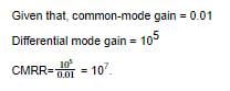
An op-amp has a common mode gain of 0.01 and a differential mode gain of 105. Its CMRR would be- a)10–7
- b)10–3
- c)103
- d)107
Correct answer is option 'D'. Can you explain this answer?
An op-amp has a common mode gain of 0.01 and a differential mode gain of 105. Its CMRR would be
a)
10–7
b)
10–3
c)
103
d)
107
| | Sarita Yadav answered |
-In electronics, the common mode rejection ratio (CMRR) of a differential amplifier (or other device) is a metric used to quantify the ability of the device to reject common-mode signals, i.e. those that appear simultaneously and in-phase on both inputs.
-
Resistivity of a semiconductor depends upon–- a)Shape nature of the semiconductor
- b)Atomic nature of the semiconductor
- c)Length of the semiconductor
- d)Shape and atomic nature of the semiconductor
Correct answer is option 'B'. Can you explain this answer?
Resistivity of a semiconductor depends upon–
a)
Shape nature of the semiconductor
b)
Atomic nature of the semiconductor
c)
Length of the semiconductor
d)
Shape and atomic nature of the semiconductor
| | Avinash Mehta answered |
Resistivity is the intrinsic property, it doesn't depend upon length and shape of the semiconductors.
It depends on atomic nature of the semiconductor.
The current ICBO flows in the- a)emitter and base leads
- b)collector and base leads.
- c)emitter and collector leads
- d)none of these
Correct answer is option 'B'. Can you explain this answer?
The current ICBO flows in the
a)
emitter and base leads
b)
collector and base leads.
c)
emitter and collector leads
d)
none of these
 | Shivam Sharma answered |
ICBO is the collector current with collector junction reverse biased and base open-circuited. ICEO is the collector current with collector junction reverse biased and emitter open-circuited. ICBO is reverse leakage current going from the Collector to the Base. This current is then amplified by β to produce additional Collector current, thus the "1+β" term.
The addition of pentavalent impurity to a semiconductor creates more–- a)Free electrons
- b)Holes
- c)Positrons
- d)Free electrons and holes
Correct answer is option 'A'. Can you explain this answer?
The addition of pentavalent impurity to a semiconductor creates more–
a)
Free electrons
b)
Holes
c)
Positrons
d)
Free electrons and holes
| | Baishali Bajaj answered |
When pentavalent impurities like phosphorus or arsenic are added into semiconductor, four electrons form bonds with the surrounding silicon atoms leaving one electron free. The resulting material has a large number of free electrons.
The Barkhausen criterion for sustained oscillations is given by- a)Ab = 1
- b)|Ab| > 1
- c)|Ab| < 1
- d)ÐAb=180º
Correct answer is option 'B'. Can you explain this answer?
The Barkhausen criterion for sustained oscillations is given by
a)
Ab = 1
b)
|Ab| > 1
c)
|Ab| < 1
d)
ÐAb=180º
| | Ishan Saini answered |
The Barkhausen criterion for sustained oscillations is a condition that must be satisfied for the circuit to produce oscillations. It is named after German physicist Heinrich Barkhausen, who first proposed the concept in 1921. The criterion states that the loop gain of the amplifier must be equal to or greater than unity and the phase shift around the loop must be a multiple of 360 degrees.
Explanation:
The Barkhausen criterion can be expressed mathematically as follows:
Ab = AβH
Where Ab is the loop gain, A is the voltage gain of the amplifier, β is the feedback factor, and H is the transfer function of the feedback network.
In order for the circuit to produce sustained oscillations, the loop gain must be equal to or greater than unity. This means that the output of the amplifier must be fed back to the input with sufficient gain to overcome losses in the circuit and maintain the oscillations.
The phase shift around the loop must be a multiple of 360 degrees. This means that the feedback signal must be in phase with the input signal at the frequency of oscillation. If the phase shift is not a multiple of 360 degrees, the oscillations will be damped out over time.
The Barkhausen criterion can be simplified to a condition that the magnitude of the loop gain must be greater than or equal to 1 and the phase shift around the loop must be an integer multiple of 360 degrees. This can be expressed mathematically as:
|Ab| ≥ 1 and Φ = 2πn
Where |Ab| is the magnitude of the loop gain, Φ is the phase shift around the loop, and n is an integer.
Conclusion:
In summary, the Barkhausen criterion is a condition that must be satisfied for a circuit to produce sustained oscillations. It requires that the loop gain be equal to or greater than unity and the phase shift around the loop be a multiple of 360 degrees. The criterion can be expressed mathematically as |Ab| ≥ 1 and Φ = 2πn.
In a common collector amplifier the voltage gain is- a)constant
- b)less than I
- c)varies with input voltage.
- d)varies with load impedance
Correct answer is option 'B'. Can you explain this answer?
In a common collector amplifier the voltage gain is
a)
constant
b)
less than I
c)
varies with input voltage.
d)
varies with load impedance
| | Niharika Basu answered |
The output voltage on a common-collector amplifier will be in phase with the input voltage, making the common-collector a non-inverting amplifier circuit. The current gain of a common-collector amplifier is equal to β plus 1. The voltage gain is approximately equal to 1 (in practice, just a little bit less).
The addition of a very small quantity of aluminium to a silicon or germanium crystal makes it–- a)A good conductor
- b)A good insulator
- c)P-type semiconductor
- d)N-type semiconductor
Correct answer is option 'C'. Can you explain this answer?
The addition of a very small quantity of aluminium to a silicon or germanium crystal makes it–
a)
A good conductor
b)
A good insulator
c)
P-type semiconductor
d)
N-type semiconductor
| | Pranab Basu answered |
Explanation:
P-type semiconductor:
When a small quantity of impurity atoms such as aluminum, boron or gallium are added to pure semiconductor materials such as silicon or germanium, it creates a material called P-type semiconductor. P-type semiconductor is created by doping a small quantity of trivalent impurity atoms in the pure semiconductor material. In P-type semiconductor, the majority carriers are holes and the minority carriers are electrons.
Working principle:
When a small quantity of aluminum is added to a silicon or germanium crystal, a P-type semiconductor is created. The aluminum atoms have only three valence electrons compared to the four valence electrons of the silicon or germanium atoms. This creates a hole in the crystal lattice structure of the silicon or germanium material.
As a result, the P-type semiconductor material has an excess of holes or positive charge carriers. When a voltage is applied across the P-type semiconductor material, these holes act as charge carriers and move towards the negative terminal of the voltage source.
Applications:
P-type semiconductor materials are widely used in the fabrication of electronic devices such as transistors, diodes, and integrated circuits. P-type semiconductors are used in the base layer of bipolar junction transistors (BJTs) and metal-oxide-semiconductor field-effect transistors (MOSFETs).
Conclusion:
Hence, the addition of a very small quantity of aluminum to a silicon or germanium crystal makes it a P-type semiconductor material. P-type semiconductors have an excess of holes or positive charge carriers, and they are widely used in electronic devices.
For a sine wave with peak value Emax the average value is –when the phase difference between the current and voltage is –- a)0.636 Emax
- b)0.707 Emax
- c)0.434 Emax
- d)1.414 Emax
Correct answer is option 'A'. Can you explain this answer?
For a sine wave with peak value Emax the average value is –when the phase difference between the current and voltage is –
a)
0.636 Emax
b)
0.707 Emax
c)
0.434 Emax
d)
1.414 Emax
| | Mahi Bose answered |
Average Value of a Sine Wave with Phase Difference
Explanation:
When a sine wave is applied to a circuit, the current and voltage may not be in phase with each other. The phase difference between the current and voltage is represented by the angle Φ.
The average value of a sine wave with peak value Emax can be calculated using the formula:
Vavg = (2/π) * Emax * sin(Φ/2)
Where Vavg is the average value of the sine wave.
To find the phase difference at which the average value is maximum, we need to differentiate this equation with respect to Φ and equate it to zero.
dVavg/dΦ = (Emax/π) * cos(Φ/2) = 0
cos(Φ/2) = 0
Φ/2 = π/2, 3π/2, 5π/2, ...
Φ = π, 3π, 5π, ...
The phase difference at which the average value is maximum is therefore Φ = π.
Substituting this value into the equation for Vavg gives:
Vavg = (2/π) * Emax * sin(π/2)
Vavg = 0.636 * Emax
Therefore, the correct option is A) 0.636 * Emax.
Conclusion:
The average value of a sine wave with peak value Emax is maximum when the phase difference between the current and voltage is π. At this phase difference, the average value is 0.636 * Emax.
Ebers-Model of transistor represents two diodes- a)in series
- b)in parallel
- c)back to back
- d)none of the above
Correct answer is option 'C'. Can you explain this answer?
Ebers-Model of transistor represents two diodes
a)
in series
b)
in parallel
c)
back to back
d)
none of the above
| | Bijoy Kapoor answered |
Ebers Moll model is a simple and elegant way of representing the transistor as a circuit model. The Ebers Moll model of transistor holds for all regions of operation of transistor. This model is based on assumption that base spreading resistance can be neglected. It will be obvious that why two diodes connected back to back will not function as a transistor from the following discussion, as dependent current source term will be missing which is responsible for all the interesting properties of transistor.
The electrical resistivity of –- a)Intrinsic semiconductor decreases with increases of temperature
- b)Intrinsic semiconductor increases with increases of temperature
- c)Metals in independent of temperature
- d)Metals decreases with increasing temperature
Correct answer is option 'A'. Can you explain this answer?
The electrical resistivity of –
a)
Intrinsic semiconductor decreases with increases of temperature
b)
Intrinsic semiconductor increases with increases of temperature
c)
Metals in independent of temperature
d)
Metals decreases with increasing temperature
| | Vidya K S answered |
Intrinsic semiconductors are not a conductivity
The emitter resistor RE is bypassed by a capacitor in order to- a)Reduce the voltage gain
- b)cause thermal run away
- c)stabilize the Q-point
- d)Increase the voltage gain
Correct answer is option 'C'. Can you explain this answer?
The emitter resistor RE is bypassed by a capacitor in order to
a)
Reduce the voltage gain
b)
cause thermal run away
c)
stabilize the Q-point
d)
Increase the voltage gain
| | Srestha Gupta answered |
Correct Answer :- C
Explanation : The main function of the emitter resistor RE bypassed by a capacitor is to improve the stability of the transistor.
Covalent bond exists in –- a)Copper
- b)NaCI crystal
- c)Silicon
- d)Arsenic
Correct answer is option 'C'. Can you explain this answer?
Covalent bond exists in –
a)
Copper
b)
NaCI crystal
c)
Silicon
d)
Arsenic
| | Baishali Bajaj answered |
The atom which has eight electrons in the outermost orbit is said to be completely filled and most stable. ... Silicon atom needs four more electrons to become most stable. Silicon atom forms four covalent bonds with the four neighboring atoms. In covalent bonding each valence electron is shared by two atoms.
In a good conductor, the energy gap between the conduction band and the valence band is –- a)Infinity
- b)Wide
- c)Narrow
- d)Zero
Correct answer is option 'D'. Can you explain this answer?
In a good conductor, the energy gap between the conduction band and the valence band is –
a)
Infinity
b)
Wide
c)
Narrow
d)
Zero
| | Nayanika Kaur answered |
Explanation:
In a good conductor, the energy gap between the conduction band and the valence band is zero. This means that the valence band and conduction band overlap, allowing electrons to move freely throughout the material.
Valence Band:
The valence band is the energy band where valence electrons are present. These electrons are bound to atoms, and they do not contribute to the electrical conductivity of the material.
Conduction Band:
The conduction band is the energy band above the valence band, where electrons can move freely. Electrons in the conduction band can conduct electricity, and this is what makes a material a good conductor.
Energy Gap:
The energy gap is the difference in energy between the valence band and the conduction band. In a good conductor, this energy gap is zero, which means that there is no energy required to move electrons from the valence band to the conduction band. This is why electrons can move freely throughout the material.
Conclusion:
In summary, the energy gap between the conduction band and the valence band is zero in a good conductor. This allows electrons to move freely throughout the material, making it a good conductor of electricity.
ICBO in transistor can be reduced by reducing- a)IB
- b)VCC
- c)IE
- d)temperature
Correct answer is option 'D'. Can you explain this answer?
ICBO in transistor can be reduced by reducing
a)
IB
b)
VCC
c)
IE
d)
temperature
| | Aditya Deshmukh answered |
ICBO is the collector current with collector junction reverse biased and base open-circuited. ICEO is the collector current with collector junction reverse biased and emitter open-circuited.
The temperature co-efficient of an intrinsic semiconductor is –- a)zero
- b)Positive
- c)Negative
- d)None of these
Correct answer is option 'C'. Can you explain this answer?
The temperature co-efficient of an intrinsic semiconductor is –
a)
zero
b)
Positive
c)
Negative
d)
None of these
 | Sukhadeep answered |
As temp increases the resist decreases -> -ve coeff
The shape of the transfer characteristic of JFET is very nearly a- a)hyperbola
- b)straight line
- c)parabola
- d)none of the above
Correct answer is option 'A'. Can you explain this answer?
The shape of the transfer characteristic of JFET is very nearly a
a)
hyperbola
b)
straight line
c)
parabola
d)
none of the above
| | Sandeep Saha answered |
Transfer Characteristic of JFET
The transfer characteristic of a JFET (Junction Field Effect Transistor) is the relationship between the input voltage (VGS) and the output current (ID). This characteristic curve is an important parameter for understanding the behavior of the JFET in different circuit configurations.
Shape of Transfer Characteristic
The shape of the transfer characteristic of a JFET is very nearly a hyperbola. A hyperbola is a curve that has two branches that are asymptotic to two intersecting lines. The transfer characteristic of a JFET is almost symmetric about the origin, and the two branches of the hyperbola represent the saturation and cutoff regions of operation.
Explanation
The transfer characteristic of a JFET can be derived from the basic equation that governs the operation of the device, known as the Shockley equation. This equation relates the drain current ID to the gate-source voltage VGS and the device parameters such as the threshold voltage Vp and the transconductance parameter gm.
ID = IDSS(1 - VGS/Vp)²
where IDSS is the maximum drain current that can flow through the device when VGS = 0.
When VGS is zero, the device is in the cutoff region and no current flows through the channel. As VGS increases, the channel resistance decreases, and the drain current ID starts to increase. When VGS reaches a certain value known as the pinch-off voltage VP, the channel resistance becomes very small, and the drain current ID reaches its maximum value IDSS.
As VGS continues to increase beyond VP, the channel resistance remains constant, and the drain current ID remains at its maximum value. This region is known as the saturation region.
The transfer characteristic of a JFET is almost symmetric about the origin, and the two branches of the hyperbola represent the saturation and cutoff regions of operation. The slope of the curve in the saturation region is determined by the transconductance parameter gm, which is a measure of the device's ability to amplify an input signal.
Conclusion
In conclusion, the transfer characteristic of a JFET is very nearly a hyperbola, and it is an important parameter for understanding the behavior of the device in different circuit configurations. The shape of the characteristic curve is determined by the basic equation that governs the operation of the JFET and its device parameters such as the threshold voltage and the transconductance parameter.
The emitter of a transistor is doped the heaviest because of it :- a)dissipates maximum power
- b)is supplier of charge carriers
- c)receives the input
- d)should have low resistance
Correct answer is option 'B'. Can you explain this answer?
The emitter of a transistor is doped the heaviest because of it :
a)
dissipates maximum power
b)
is supplier of charge carriers
c)
receives the input
d)
should have low resistance
| | Aisha Gupta answered |
The reason the emitter is the most heavily doped region is because it serves to inject a large amount of charge carriers into the base, which then travels into the collector, so that switching or amplification can occur.
The energy band gap of silicon is –- a)0.72 eV
- b)1.1 eV
- c)6 eV
- d)Between 0.72 to 1.1 eV
Correct answer is option 'B'. Can you explain this answer?
The energy band gap of silicon is –
a)
0.72 eV
b)
1.1 eV
c)
6 eV
d)
Between 0.72 to 1.1 eV
| | Sharmila Kulkarni answered |
Energy Band Gap of Silicon
Introduction:
Silicon is the most widely used semiconductor material in the electronics industry due to its excellent electrical and physical properties.
Energy Band Gap:
The energy band gap is the energy difference between the valence band and the conduction band. It is a critical parameter that determines the electrical properties of a semiconductor material.
Energy Band Gap of Silicon:
The energy band gap of silicon is 1.1 eV. This means that it requires 1.1 eV of energy to break an electron free from the valence band and move it to the conduction band.
Significance:
The energy band gap of silicon is of great significance in the electronics industry as it determines the minimum energy required to excite electrons from the valence band to the conduction band. This, in turn, affects the conductivity and other electrical properties of the material.
Applications:
The energy band gap of silicon makes it suitable for a wide range of applications, including:
- Solar cells
- Transistors
- Integrated circuits
- Light-emitting diodes (LEDs)
- Sensors
Conclusion:
In conclusion, the energy band gap of silicon is 1.1 eV, and this property makes it a widely used semiconductor material in the electronics industry.
All the rules and laws of D.C. circuit also supply to A.C. circuit containing–- a)Capacitance only
- b)Inductance only
- c)Resistance only
- d)All above
Correct answer is option 'C'. Can you explain this answer?
All the rules and laws of D.C. circuit also supply to A.C. circuit containing–
a)
Capacitance only
b)
Inductance only
c)
Resistance only
d)
All above
| | Amar Sengupta answered |
Understanding D.C. and A.C. Circuits
In electrical engineering, D.C. (Direct Current) circuits and A.C. (Alternating Current) circuits have distinct behaviors and governing laws. The distinction primarily lies in how different components affect current flow.
Resistance in Circuits
- D.C. circuits obey Ohm's Law, where voltage (V), current (I), and resistance (R) are related by the formula V = I × R.
- Resistance is a passive component that opposes current flow, and its effect is the same in both D.C. and A.C. circuits.
- Therefore, all laws applicable to resistance in D.C. circuits also apply to A.C. circuits.
Capacitance and Inductance in A.C. Circuits
- Capacitors and inductors behave differently in A.C. circuits compared to D.C. circuits.
- In a D.C. circuit, a capacitor will charge to a certain voltage and then block further current flow, while an inductor will resist changes in current but does not affect steady-state D.C.
- In A.C. circuits, capacitors and inductors introduce phase shifts and reactance, making them essential for understanding circuit behavior but not directly comparable to resistance laws.
Conclusion
- Thus, the statement that "all the rules and laws of D.C. circuits also apply to A.C. circuits containing resistance only" holds true.
- Capacitance and inductance introduce complexities that are not present in D.C. circuits, making the application of their rules in A.C. circuits distinct.
In summary, only resistance retains the same governing rules across both types of circuits, affirming that the correct answer is option 'C'.
Which of the following is not a semiconductor?- a)Silicon
- b)Germanium
- c)Arsenic
- d)Selenium
Correct answer is option 'C'. Can you explain this answer?
Which of the following is not a semiconductor?
a)
Silicon
b)
Germanium
c)
Arsenic
d)
Selenium
| | Sagarika Patel answered |
The semiconductor industry, this process is commonly referred to as “doping.” Arsenic, phosphorus, antimony and boron are all used for doping semiconductors. These elements each produce unique electrical conductivity properties when used as dopants. As a result, they are not interchangeable.
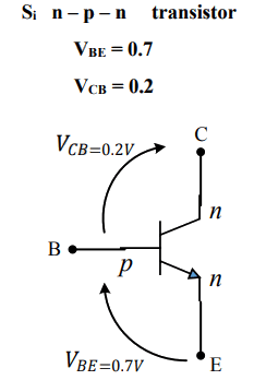
In cutoff region in an N-P-N transistor- a)VCB is + Ve and VBE is – ve
- b)VCB is – ve and VBE is + ve
- c)Both VCB and VBE are positive
- d)Both VCB and VBE are negative
Correct answer is option 'A'. Can you explain this answer?
In cutoff region in an N-P-N transistor
a)
VCB is + Ve and VBE is – ve
b)
VCB is – ve and VBE is + ve
c)
Both VCB and VBE are positive
d)
Both VCB and VBE are negative
 | Rahul Chatterjee answered |
Whenever we observe the terminals of a BJT and see that the emitter-base junction is not at least 0.6-0.7 volts, the transistor is in the cutoff region. In cutoff, the transistor appears as an open circuit between the collector and emitter terminals. As is seen in 2, this implies Vout is equal to 10 volts.
The BJT amplifier which offers highest input impedance and least voltage gain is- a)CE
- b)CB
- c)CC
- d)Cascode amplifier
Correct answer is option 'C'. Can you explain this answer?
The BJT amplifier which offers highest input impedance and least voltage gain is
a)
CE
b)
CB
c)
CC
d)
Cascode amplifier
| | Arindam Sengupta answered |
BJT Amplifiers
BJT (Bipolar Junction Transistor) amplifiers are designed to amplify signals in electronic devices. There are three types of BJT amplifiers: Common Emitter (CE), Common Base (CB), and Common Collector (CC).
Input Impedance and Voltage Gain
Input impedance refers to the measure of how much an amplifier resists the flow of signals into the input terminals, while voltage gain refers to the measure of how much an amplifier increases the voltage of an input signal.
CE, CB, and CC amplifiers all have different input impedance and voltage gain values. However, the CC amplifier offers the highest input impedance and the least voltage gain among the three types.
Cascode Amplifier
A cascode amplifier is a two-stage amplifier that combines the CE and CC amplifiers to improve their performance. It offers high input impedance and high voltage gain, making it an excellent choice for RF (Radio Frequency) applications.
However, the cascode amplifier requires extra components and is more complicated to design and implement than the CE, CB, and CC amplifiers.
Conclusion
In summary, the CC amplifier offers the highest input impedance and the least voltage gain among the three types of BJT amplifiers. The cascode amplifier, on the other hand, offers high input impedance and high voltage gain but requires more components and is more complicated to design and implement.
Application of DC voltage to a diode, transistor, or other device to produce a desired mode of operation is called- a)biasing
- b)reduction
- c)bounding
- d)modulation
Correct answer is option 'A'. Can you explain this answer?
Application of DC voltage to a diode, transistor, or other device to produce a desired mode of operation is called
a)
biasing
b)
reduction
c)
bounding
d)
modulation
| | Kiran Iyer answered |
Explanation:
Biasing is the process of applying DC voltage to a diode, transistor, or other device to produce a desired mode of operation. It is an essential process in electronic circuits that allows devices to work correctly under specific conditions. The DC voltage applied to the device is called the bias voltage, and it determines the operating point of the device. The bias voltage affects the voltage and current levels of the device, which, in turn, affects its behavior.
Importance of Biasing:
Biasing is a critical process in electronic circuits, and it is essential for the following reasons:
- It sets the operating point of the device, which affects its behavior and performance.
- It ensures that the device operates within its safe operating range.
- It prevents the device from being damaged due to excessive voltage or current.
- It improves the stability and reliability of the circuit.
Types of Biasing:
There are different types of biasing techniques used in electronic circuits, some of them are:
- Fixed Biasing
- Self-Biasing
- Voltage Divider Biasing
- Emitter Biasing
- Collector-to-Base Biasing
Conclusion:
Biasing is a crucial process in electronic circuits that involves applying a DC voltage to a device to produce a desired mode of operation. It is essential for setting the operating point of the device, ensuring its safe operation, and improving the stability and reliability of the circuit. Different types of biasing techniques are used in electronic circuits depending on the application and device used.
Which one of the following specifications is not correct for a common collector amplifier ?- a)High input impedance
- b)Low output impedance
- c)High voltage gain
- d)High current gain
Correct answer is option 'C'. Can you explain this answer?
Which one of the following specifications is not correct for a common collector amplifier ?
a)
High input impedance
b)
Low output impedance
c)
High voltage gain
d)
High current gain
| | Raghav Majumdar answered |
Common Collector Amplifier
A common collector amplifier is also known as an emitter follower. It is a type of transistor amplifier circuit in which the collector terminal of the transistor is common to both the input and output signals. The emitter terminal is used as the output while the base terminal is used as the input.
Specifications of Common Collector Amplifier
- High input impedance: The input impedance of a common collector amplifier is very high. This is because the input signal is applied to the base terminal of the transistor, which has a very high impedance.
- Low output impedance: The output impedance of a common collector amplifier is very low. This is because the output signal is taken from the emitter terminal, which has a very low impedance.
- High current gain: The current gain of a common collector amplifier is very high. This is because the emitter current is almost equal to the collector current.
- Incorrect specification: High voltage gain is not a correct specification for a common collector amplifier. This is because the voltage gain of a common collector amplifier is always less than 1. This means that the output voltage is always less than the input voltage.
Conclusion
In summary, a common collector amplifier has a high input impedance, low output impedance, and high current gain. However, it does not have a high voltage gain.


............... are immobile.- a)Electrons
- b)Ions
- c)Holes
- d)None of these
Correct answer is option 'B'. Can you explain this answer?
............... are immobile.
a)
Electrons
b)
Ions
c)
Holes
d)
None of these
| | Mahesh Datta answered |
I'm sorry, I need more information or context to understand what you are asking for. Can you please provide more details or a specific question?
The action of a JFET in its equivalent circuit can best be represented as a- a)Current Controlled Current source
- b)Current Controlled Voltage Source
- c)Voltage Controlled Voltage source
- d)Voltage Controlled Current Source
Correct answer is option 'D'. Can you explain this answer?
The action of a JFET in its equivalent circuit can best be represented as a
a)
Current Controlled Current source
b)
Current Controlled Voltage Source
c)
Voltage Controlled Voltage source
d)
Voltage Controlled Current Source
| | Prateek Mehra answered |
The JFET Action Explained
The Junction Field Effect Transistor (JFET) operates primarily as a voltage-controlled device. Its equivalent circuit representation is crucial for understanding its functionality.
Voltage Controlled Current Source
- The JFET uses a voltage applied to its gate terminal to control the current flowing through its drain-source channel.
- The gate-source voltage (Vgs) influences the conductivity of the channel, making it a voltage-controlled device.
Current Flow Mechanism
- When a negative voltage is applied to the gate (for an n-channel JFET), it repels charge carriers (electrons), reducing the channel's conductivity.
- Conversely, a zero or positive voltage increases the channel’s conductivity, allowing more current to flow from the drain to the source.
Comparison with Other Sources
- Current Controlled Current Source: This would imply that output current is controlled by input current, which is not the case in JFETs.
- Current Controlled Voltage Source: Does not apply, as JFET operation relies on voltage to control current, not vice versa.
- Voltage Controlled Voltage Source: While JFET gates respond to voltage, the output current is not directly linked to an output voltage in this manner.
Conclusion
- In summary, the JFET acts as a Voltage Controlled Current Source because the gate voltage controls the amount of drain current flowing through the device.
- This characteristic is fundamental to its applications in amplification and switching circuits.
In A.C. circuit the power curve is a sine wave having–- a)Double the frequency of voltage
- b)Same frequency as that of voltage
- c)Half the frequency of the voltage
- d)None of these
Correct answer is option 'A'. Can you explain this answer?
In A.C. circuit the power curve is a sine wave having–
a)
Double the frequency of voltage
b)
Same frequency as that of voltage
c)
Half the frequency of the voltage
d)
None of these
| | Shivam Ghosh answered |
Understanding Power in A.C. Circuits
In an Alternating Current (A.C.) circuit, the relationship between voltage and power can be complex. One essential aspect is how the power waveform behaves in relation to the voltage waveform.
Frequency of Power vs. Voltage
- The power in an A.C. circuit is calculated using the formula:
- P(t) = V(t) * I(t)
- Here, V(t) is the voltage waveform and I(t) is the current waveform.
Voltage and Current Waveforms
- In a purely resistive circuit:
- Voltage (V) and current (I) are in phase, meaning they reach their maximum and minimum values simultaneously.
- In inductive or capacitive circuits:
- The current lags or leads the voltage, respectively.
Power Waveform Characteristics
- The product of two sinusoidal functions (voltage and current) produces a waveform that is not merely a sine wave.
- When you multiply two sine waves of the same frequency, the resulting waveform contains terms that double the frequency due to the trigonometric identity:
- sin(A) * sin(B) = 0.5 [cos(A-B) - cos(A+B)]
- Thus, the power waveform has components at twice the frequency of the original sine wave voltages and currents.
Conclusion
- Therefore, in A.C. circuits, the power curve indeed has a frequency that is double that of the voltage waveform, confirming that the correct answer is option 'A'.
This understanding is crucial for analyzing and designing A.C. electrical systems efficiently.
Chapter doubts & questions for Basic Electronics - Electrical Engineering SSC JE (Technical) 2026 is part of Electrical Engineering (EE) exam preparation. The chapters have been prepared according to the Electrical Engineering (EE) exam syllabus. The Chapter doubts & questions, notes, tests & MCQs are made for Electrical Engineering (EE) 2026 Exam. Find important definitions, questions, notes, meanings, examples, exercises, MCQs and online tests here.
Chapter doubts & questions of Basic Electronics - Electrical Engineering SSC JE (Technical) in English & Hindi are available as part of Electrical Engineering (EE) exam. Download more important topics, notes, lectures and mock test series for Electrical Engineering (EE) Exam by signing up for free.
Electrical Engineering SSC JE (Technical)23 videos|95 docs|42 tests |