


All Exams > Electrical Engineering (EE) > Analog and Digital Electronics > All Questions
All questions of Simple Diode Circuits for Electrical Engineering (EE) Exam
The diode in a half wave rectifier has a forward resistance RF. The voltage is Vmsinωt and the load resistance is RL. The DC current is given by _________- a)Vm/√2RL
- b)Vm/(RF+RL)π
- c)2Vm/√π
- d)Vm/RL
Correct answer is option 'B'. Can you explain this answer?
The diode in a half wave rectifier has a forward resistance RF. The voltage is Vmsinωt and the load resistance is RL. The DC current is given by _________
a)
Vm/√2RL
b)
Vm/(RF+RL)π
c)
2Vm/√π
d)
Vm/RL
| | Bibek Saha answered |
For a half wave rectifier, the IDC=IAVG=Im/π
I= Vmsinωt/(RF+RL)=Imsinωt
Im =Vm/ RF+RL So, IDC=Im/π=Vm/(RF+RL).
I= Vmsinωt/(RF+RL)=Imsinωt
Im =Vm/ RF+RL So, IDC=Im/π=Vm/(RF+RL).

A full wave rectifier uses load resistor of 1500Ω. Assume the diodes have Rf=10Ω, Rr=∞. The voltage applied to diode is 30V with a frequency of 50Hz. Calculate the AC power input.- a)368.98mW
- b)275.2mW
- c)145.76mW
- d)456.78mW
Correct answer is option 'B'. Can you explain this answer?
A full wave rectifier uses load resistor of 1500Ω. Assume the diodes have Rf=10Ω, Rr=∞. The voltage applied to diode is 30V with a frequency of 50Hz. Calculate the AC power input.
a)
368.98mW
b)
275.2mW
c)
145.76mW
d)
456.78mW
 | Nidhi Tiwari answered |
The AC power input PIN=IRMS2(RF+Rr).
IRMS=Im/√2=Vm/(Rf+RL)√2=30/(1500+10)*1.414=13.5mA
So, PIN=(13.5*10-3)2*(1500+10)=275.2mW.
IRMS=Im/√2=Vm/(Rf+RL)√2=30/(1500+10)*1.414=13.5mA
So, PIN=(13.5*10-3)2*(1500+10)=275.2mW.
Efficiency of a half wave rectifier is- a)50%
- b)60%
- c)40.6%
- d)46%
Correct answer is option 'C'. Can you explain this answer?
Efficiency of a half wave rectifier is
a)
50%
b)
60%
c)
40.6%
d)
46%
| | Sakshi Tiwari answered |
Efficiency of a Half Wave Rectifier
Introduction:
A half wave rectifier is a circuit that converts an alternating current (AC) input signal into a direct current (DC) output signal. It uses a diode as a rectifying element to allow current flow in only one direction. The efficiency of a rectifier is a measure of how effectively it converts AC power to DC power.
Efficiency Formula:
The efficiency of a rectifier is calculated using the formula:
Efficiency = (DC Power Output / AC Power Input) * 100%
The DC Power Output is the power delivered to the load, and the AC Power Input is the power supplied by the AC source.
Efficiency Calculation for a Half Wave Rectifier:
In a half wave rectifier, the AC input signal is applied across a diode and a load resistor. The diode conducts current only during the positive half cycles of the input signal, blocking the negative half cycles. This results in a pulsating DC output signal.
1. DC Power Output Calculation:
The DC power output can be calculated using the formula:
DC Power Output = (Vrms^2) / RL
Where Vrms is the root mean square value of the output voltage and RL is the load resistance.
2. AC Power Input Calculation:
The AC power input can be calculated using the formula:
AC Power Input = (Vrms^2) / RL
Where Vrms is the root mean square value of the input voltage and RL is the load resistance.
3. Efficiency Calculation:
Substituting the values in the efficiency formula, we get:
Efficiency = [(Vrms^2) / RL] / [(Vrms^2) / RL] * 100%
Simplifying the equation, we find:
Efficiency = 50% * (RL / RL)
The load resistance RL cancels out, resulting in an efficiency of 50%.
Conclusion:
The efficiency of a half wave rectifier is 50% because it conducts current only during the positive half cycles of the input signal, resulting in a pulsating DC output. This means that half of the AC power is wasted or not utilized effectively, leading to an efficiency of 50%.
A full wave rectifier supplies a load of 1KΩ. The AC voltage applied to diodes is 220V (rms). If diode resistance is neglected, what is the ripple voltage?- a)0.562V
- b)78.5V
- c)95.4V
- d)0.344V
Correct answer is option 'C'. Can you explain this answer?
A full wave rectifier supplies a load of 1KΩ. The AC voltage applied to diodes is 220V (rms). If diode resistance is neglected, what is the ripple voltage?
a)
0.562V
b)
78.5V
c)
95.4V
d)
0.344V
 | EduRev GATE answered |
Explanation: The ripple voltage (Vϒ)RMS = ϒ * VDC.
Here ϒ is ripple factor of a full wave rectifier and it is 0.482.
Here ϒ is ripple factor of a full wave rectifier and it is 0.482.
VDC = (2/π) * VRMS* √2 = 0.636 * 220 * √2 = 198V
Hence, (Vϒ)RMS = 0.482 * 198 = 95.4V.
Hence, (Vϒ)RMS = 0.482 * 198 = 95.4V.
Transformer utilisation factor of a half wave rectifier is _________- a)0.234
- b)0.279
- c)0.287
- d)0.453
Correct answer is option 'C'. Can you explain this answer?
Transformer utilisation factor of a half wave rectifier is _________
a)
0.234
b)
0.279
c)
0.287
d)
0.453
 | Neha Basak answered |
Transformer utilisation factor is the ratio of AC power delivered to load to the DC power rating. This factor indicates effectiveness of transformer usage by rectifier. For a half wave rectifier, it’s low and equal to 0.287.
Determine the minimum value of load resistance that can be used in the circuit with (IZ)Min=3mA. The input voltage is 10V and the resistance R is 500Ω. The Zener diode has a VZ=6V 0and (IZ)MAX=90mA.- a)1KΩ
- b)2.4KΩ
- c)1.2KΩ
- d)3.6KΩ
Correct answer is option 'C'. Can you explain this answer?
Determine the minimum value of load resistance that can be used in the circuit with (IZ)Min=3mA. The input voltage is 10V and the resistance R is 500Ω. The Zener diode has a VZ=6V 0and (IZ)MAX=90mA.
a)
1KΩ
b)
2.4KΩ
c)
1.2KΩ
d)
3.6KΩ
 | Asha Nambiar answered |
The I=(VIN-VZ)/R=(10-6)/500=8mA. (IL)MAX=I-(IZ)MIN=8-3=5mA. (RL)MIN=VZ/(IL)MAX=6/5m=1.2KΩ.
The percentage voltage regulation (VL) is given by_________- a)(VNL-VL)/VNL*100
- b)(VNL+VL)/VNL*100
- c)(VNL-VL)/VL*100
- d)(VNL+VL)/VL*100
Correct answer is option 'A'. Can you explain this answer?
The percentage voltage regulation (VL) is given by_________
a)
(VNL-VL)/VNL*100
b)
(VNL+VL)/VNL*100
c)
(VNL-VL)/VL*100
d)
(VNL+VL)/VL*100
| | Swati Shah answered |
The change in the output voltage from no load to full load condition is called as voltage regulation, where VNL is the voltage at no load condition. It is used to maintain a nearly constant output voltage. If the regulation is high, the output voltage is stable.
In a half wave rectifier, the sine wave input is 200sin300t. The average value of output voltage is?- a)57.876V
- b)67.453V
- c)63.694V
- d)76.987V
Correct answer is option 'C'. Can you explain this answer?
In a half wave rectifier, the sine wave input is 200sin300t. The average value of output voltage is?
a)
57.876V
b)
67.453V
c)
63.694V
d)
76.987V
 | Sonal Tiwari answered |
Comparing with the standard equation, Vm=200V.
Average value is given by, Vavg=Vm/π.
So, 200/π=63.694.
Average value is given by, Vavg=Vm/π.
So, 200/π=63.694.
In a half wave rectifier, the sine wave input is 50sin50t. If the load resistance is of 1K, then average DC power output will be?- a)3.99V
- b)2.5V
- c)5.97V
- d)6.77V
Correct answer is option 'B'. Can you explain this answer?
In a half wave rectifier, the sine wave input is 50sin50t. If the load resistance is of 1K, then average DC power output will be?
a)
3.99V
b)
2.5V
c)
5.97V
d)
6.77V
 | Charvi Kaur answered |
The standard form of a sine wave is Vmsinωt. BY comparing the given information with this equation, Vm =50.
Power=Vm2/RL=50*50/1000=2.5V.
Power=Vm2/RL=50*50/1000=2.5V.
If the peak voltage on a centre tapped full wave rectifier circuit is 5V and diode cut in voltage is 0.7. The peak inverse voltage on diode is_________- a)4.3V
- b)9.3V
- c)5.7V
- d)10.7V
Correct answer is option 'B'. Can you explain this answer?
If the peak voltage on a centre tapped full wave rectifier circuit is 5V and diode cut in voltage is 0.7. The peak inverse voltage on diode is_________
a)
4.3V
b)
9.3V
c)
5.7V
d)
10.7V
 | Bhargavi Kulkarni answered |
PIV is the maximum reverse bias voltage that can be appeared across a diode in the given circuit, if PIV rating is less than this value of breakdown of diode will occur. For a rectifier, PIV=2Vm-Vd = 10-0.7 = 9.3V.
Efficiency of a centre tapped full wave rectifier is _________- a)50%
- b)46%
- c)70%
- d)81.2%
Correct answer is option 'D'. Can you explain this answer?
Efficiency of a centre tapped full wave rectifier is _________
a)
50%
b)
46%
c)
70%
d)
81.2%
 | Arshiya Dasgupta answered |
Efficiency of a rectifier is the effectiveness to convert AC to DC. It’s obtained by taking ratio of DC power output to maximum AC power delivered to load. It’s usually expressed in percentage. For centre tapped full wave rectifier, it’s 81.2%.
If peak voltage for a half wave rectifier circuit is 5V and diode cut in voltage is 0.7, then peak inverse voltage on diode will be?- a)5V
- b)4.9V
- c)4.3V
- d)6.7V
Correct answer is option 'C'. Can you explain this answer?
If peak voltage for a half wave rectifier circuit is 5V and diode cut in voltage is 0.7, then peak inverse voltage on diode will be?
a)
5V
b)
4.9V
c)
4.3V
d)
6.7V
| | Aashna Dey answered |
PIV is the maximum reverse bias voltage that can be appeared across a diode in the given circuit, If the PIV rating is less than this value of breakdown of diode will occur. For a rectifier, PIV=Vm-Vd=5-0.7=4.3V.
A full wave rectifier delivers 50W to a load of 200Ω. If the ripple factor is 2%, calculate the AC ripple across the load.- a)2V
- b)5V
- c)4V
- d)1V
Correct answer is option 'A'. Can you explain this answer?
A full wave rectifier delivers 50W to a load of 200Ω. If the ripple factor is 2%, calculate the AC ripple across the load.
a)
2V
b)
5V
c)
4V
d)
1V
| | Gaurav Chauhan answered |
We know that, PDC=VDC2/RL. So, VDC=(PDC*RL)1/2=100001/2=100V.
Here, ϒ=0.02
ϒ=VAC/VDC=VAC/100.So, VAC=0.02*100=2V.
Here, ϒ=0.02
ϒ=VAC/VDC=VAC/100.So, VAC=0.02*100=2V.
When is a regulator used?- a)when there are small variations in load current and input voltage
- b)when there are large variations in load current and input voltage
- c)when there are no variations in load current and input voltage
- d)when there are small variations in load current and large variations in input voltage
Correct answer is option 'A'. Can you explain this answer?
When is a regulator used?
a)
when there are small variations in load current and input voltage
b)
when there are large variations in load current and input voltage
c)
when there are no variations in load current and input voltage
d)
when there are small variations in load current and large variations in input voltage
 | Mira Mishra answered |
The regulator has following limitations: 1.It has low efficiency for heavy load currents 2. The output voltage changes slightly due to Zener impedance. Hence, it is used when there are small variations in load current and input voltage.
Transformer utilization factor of a centre tapped half wave rectifier is_________- a)0.623
- b)0.678
- c)0.693
- d)0.625
Correct answer is option 'C'. Can you explain this answer?
Transformer utilization factor of a centre tapped half wave rectifier is_________
a)
0.623
b)
0.678
c)
0.693
d)
0.625
| | Aniket Shah answered |
Understanding Transformer Utilization Factor (TUF)
The Transformer Utilization Factor (TUF) is a measure used in electrical engineering to assess how effectively a transformer is being utilized. It is particularly relevant in rectifier circuits, such as a center-tapped half-wave rectifier.
Definition of TUF
- TUF is defined as the ratio of the DC output power to the AC input power.
- In half-wave rectifiers, TUF helps determine the efficiency of transformer usage.
Calculating TUF for Center-Tapped Half-Wave Rectifier
- In a center-tapped half-wave rectifier, the transformer is utilized only during one half of the AC cycle.
- The effective output DC voltage (V_dc) can be calculated, and the load resistance (R) is considered to find the output power.
- For a center-tapped transformer, the average output voltage (V_avg) is given as V_m/π, where V_m is the peak voltage.
Derivation of TUF Value
- The TUF for a center-tapped half-wave rectifier is derived as follows:
- Output Power (P_dc) = V_dc²/R
- Input Power (P_ac) = (V_rms²)/(R)
- By substituting and simplifying, we find TUF = P_dc / P_ac = 0.693, leading to the answer.
Conclusion
- Therefore, the Transformer Utilization Factor for a center-tapped half-wave rectifier is 0.693, making option 'C' the correct answer.
- This indicates that the transformer is utilized effectively, providing a balance between output power and transformer capacity.
Understanding TUF is essential for designing efficient rectifier circuits and ensuring optimal transformer performance in electrical systems.
Which of the following is not a necessary component in a clamper circuit?- a)Diode
- b)Capacitor
- c)Resistor
- d)Independent DC Supply
Correct answer is option 'D'. Can you explain this answer?
Which of the following is not a necessary component in a clamper circuit?
a)
Diode
b)
Capacitor
c)
Resistor
d)
Independent DC Supply
| | Tanya Chauhan answered |
In a clamper circuit, the primary purpose is to shift the DC level of the input signal without altering the shape of the signal. This is achieved by adding a DC bias to the input signal. The necessary components in a clamper circuit include a diode, a capacitor, and a resistor.
- Diode: The diode is an essential component in a clamper circuit as it allows the flow of current in one direction while blocking it in the opposite direction. It helps in shifting the DC level of the input signal by allowing the capacitor to charge or discharge through it.
- Capacitor: The capacitor is another necessary component in a clamper circuit. It is connected in parallel to the diode and is charged or discharged depending on the input signal. The capacitor stores the charge and releases it during the negative half-cycle of the input signal, thereby shifting the DC level of the signal.
- Resistor: The resistor is also an important component in a clamper circuit. It is connected in series with the diode and capacitor. The resistor limits the current flowing through the circuit and helps in stabilizing the voltage across the capacitor.
- Independent DC Supply: The independent DC supply is not a necessary component in a clamper circuit. It is not required because the purpose of a clamper circuit is to shift the DC level of the input signal using the existing components. The diode, capacitor, and resistor work together to achieve this without the need for an additional DC supply.
Therefore, the correct answer is option 'D' - Independent DC Supply.
For the given circuit for a 20 Vpeak sinusoidal input vi, what is the value of vi at which the clipping begins?
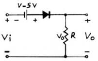
- a)5 V
- b)0 V
- c)-5 V
- d)Clipping doesn’t occur
Correct answer is option 'C'. Can you explain this answer?
For the given circuit for a 20 Vpeak sinusoidal input vi, what is the value of vi at which the clipping begins?
a)
5 V
b)
0 V
c)
-5 V
d)
Clipping doesn’t occur
 | Ankit Mukherjee answered |
It is not possible to determine the value of vi at which the clipping begins without additional information about the circuit. The clipping voltage depends on the specific characteristics and parameters of the circuit, such as the diode threshold voltage or the supply voltage.
A transistor series regulator has the following specifications: VIN=15V, VZ=8.3V, β=100, R=1.8KΩ, RL=2KΩ. What will be the Zener current in the regulator circuit?- a)4.56mA
- b)3.26mA
- c)3.68mA
- d)none
Correct answer is option 'C'. Can you explain this answer?
A transistor series regulator has the following specifications: VIN=15V, VZ=8.3V, β=100, R=1.8KΩ, RL=2KΩ. What will be the Zener current in the regulator circuit?
a)
4.56mA
b)
3.26mA
c)
3.68mA
d)
none
| | Asha Nambiar answered |
We know, VO=VZ-VBE=8.3-0.7=7.6V. VCE=VIN-V0=15-7.6=7.4V. So, IR=(VIN-VZ)/R=(15-8.3)/1.8m=3.72mA. IL=VO/RL=7.6/2000=3.8mA. IB=IL/ β=3.8mA/100=0.038mA. Finally, IZ=IR-IB=3.72-0.038=3.682mA.
A transistor in a series voltage regulator acts like a variable resistor. The value of its resistance is determined by _______- a)emitter current
- b)base current
- c)collector current
- d)it is not controlled by the transistor terminals
Correct answer is option 'B'. Can you explain this answer?
A transistor in a series voltage regulator acts like a variable resistor. The value of its resistance is determined by _______
a)
emitter current
b)
base current
c)
collector current
d)
it is not controlled by the transistor terminals
 | Jaya Yadav answered |
The principle is based on the fact that a large fraction of the increase in input voltage appears across the transistor so that the output voltage remains to be constant. When input voltage is increased, the output voltage also increases which biases the transistor towards less current.
Determine the maximum and minimum values of load current for which the Zener diode shunt regulator will maintain regulation when VIN=24V and R=500Ω. The Zener diode has a VZ=12V and (IZ)MAX=90mA.- a)40mA, 0mA respectively
- b)36mA, 5mA respectively
- c)10mA, 6mA respectively
- d)21mA, 0mA respectively
Correct answer is option 'D'. Can you explain this answer?
Determine the maximum and minimum values of load current for which the Zener diode shunt regulator will maintain regulation when VIN=24V and R=500Ω. The Zener diode has a VZ=12V and (IZ)MAX=90mA.
a)
40mA, 0mA respectively
b)
36mA, 5mA respectively
c)
10mA, 6mA respectively
d)
21mA, 0mA respectively
| | Jaya Dasgupta answered |
The current through the resistance R is given by, I=(VIN-VZ)/R= (24-12)/500=24mA. (IL)MAX=I-(IZ)MIN=24-3=21mA .This current is less than (IZ)MAX. So, we assume that all the input current flows through the Zener diode. Under this condition, (IL)MINis 0mA.
In a centre tapped full wave rectifier, the input sine wave is 250sin100t. The output ripple frequency will be _________- a)50Hz
- b)100Hz
- c)25Hz
- d)200Hz
Correct answer is option 'B'. Can you explain this answer?
In a centre tapped full wave rectifier, the input sine wave is 250sin100t. The output ripple frequency will be _________
a)
50Hz
b)
100Hz
c)
25Hz
d)
200Hz
 | Srishti Chopra answered |
The equation of sine wave is in the form Vmsinωt. So, by comparing we get ω=100. Frequency, f =ω/2=50Hz. The output of centre tapped full wave rectifier has double the frequency of inpu. Hence, fout = 100Hz.
A Zener regulator has to handle supply voltage variation from 19.5V to 22.5V. Find the magnitude of regulating resistance, if the load resistance is 6KΩ. The Zener diode has the following specifications: breakdown voltage =18V, (IZ)Min=2µA, maximum power dissipation=60mW and Zener resistance =20Ω.- a)0 < R < 500Ω
- b)77.8 < R < 500Ω
- c)77.8 < R < 100Ω
- d)18 < R < 500Ω
Correct answer is option 'B'. Can you explain this answer?
A Zener regulator has to handle supply voltage variation from 19.5V to 22.5V. Find the magnitude of regulating resistance, if the load resistance is 6KΩ. The Zener diode has the following specifications: breakdown voltage =18V, (IZ)Min=2µA, maximum power dissipation=60mW and Zener resistance =20Ω.
a)
0 < R < 500Ω
b)
77.8 < R < 500Ω
c)
77.8 < R < 100Ω
d)
18 < R < 500Ω
 | Saptarshi Nair answered |
(PZ)MAX/rZ=(IZ)MAX2 . So, (IZ)MAX =60m/20=54.8µA. IL=VO/RL=18/6000=3mA.
RMAX=(VMin-VZ)/[( IZ)Min+( IL)MAX]=(19.5-18)/(2µ+3m)=500Ω.
RMin=(VMAX-VZ)/[( IZ)MAX+( IL)Min]=(22.5-18)/(54.8m+3m)=77.8Ω.
RMAX=(VMin-VZ)/[( IZ)Min+( IL)MAX]=(19.5-18)/(2µ+3m)=500Ω.
RMin=(VMAX-VZ)/[( IZ)MAX+( IL)Min]=(22.5-18)/(54.8m+3m)=77.8Ω.
Ripple factor of a half wave rectifier is_________(Im is the peak current and RL is load resistance)- a)1.414
- b)1.21
- c)1.4
- d)e)a) 1.414b) 1.21c) 1.4
Correct answer is option 'B'. Can you explain this answer?
Ripple factor of a half wave rectifier is_________(Im is the peak current and RL is load resistance)
a)
1.414
b)
1.21
c)
1.4
d)
e)a) 1.414b) 1.21c) 1.4
 | Kiran Gupta answered |
The ripple factor of a rectifier is the measure of disturbances produced in the output. It’s the effectiveness of a power supply filter to reduce the ripple voltage. The ratio of ripple voltage to DC output voltage is ripple factor which is 1.21.
The limiting value of the current resistor used in a Zener diode (when used as a regulator)- a)(R)min=[(Vin)max + VZ/R
- b)(R)min=[(Vin)max-VZ]/R
- c)(R)min=[(Vin)max-VZ]R
- d) (R)min=[(Vin)max+ VZ]R
Correct answer is option 'B'. Can you explain this answer?
The limiting value of the current resistor used in a Zener diode (when used as a regulator)
a)
(R)min=[(Vin)max + VZ/R
b)
(R)min=[(Vin)max-VZ]/R
c)
(R)min=[(Vin)max-VZ]R
d)
(R)min=[(Vin)max+ VZ]R
 | Shreya Choudhary answered |
When the input voltage is maximum, the load current is minimum, the Zener current should not increase the maximum rated value. Therefore there should be a minimum value of resistor.
If input frequency is 50Hz for a full wave rectifier, the ripple frequency of it would be _________- a)100Hz
- b)50Hz
- c)25Hz
- d)500Hz
Correct answer is option 'A'. Can you explain this answer?
If input frequency is 50Hz for a full wave rectifier, the ripple frequency of it would be _________
a)
100Hz
b)
50Hz
c)
25Hz
d)
500Hz
 | Tanvi Sarkar answered |
In the output of the centre tapped rectifier, one of the half cycle is repeated. The frequency will be twice as that of input frequency. So, it’s 100Hz.
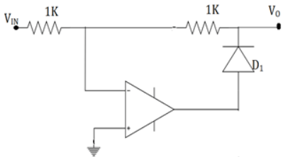
The below figure arrives to a conclusion that _________
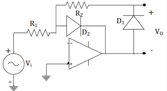
- a)for Vi > 0, V0=-(R2/R1)Vi
- b) for Vi > 0, V0=0
- c)Vi < 0, V0=-(R2/R1)Vi
- d)Vi < 0, V0=0
Correct answer is option 'B'. Can you explain this answer?
The below figure arrives to a conclusion that _________
a)
for Vi > 0, V0=-(R2/R1)Vi
b)
for Vi > 0, V0=0
c)
Vi < 0, V0=-(R2/R1)Vi
d)
Vi < 0, V0=0
| | Juhi Joshi answered |
The given op-amp is in inverting mode and this makes the output voltage to have a phase shift of 180°. The output voltage is now negative. So, the diode 1 is reverse biased and diode 2 is forward biased. Then output is clearly zero.
In the given limiter circuit, an input voltage Vi=10sin100πt is applied. Assume that the diode drop is 0.7V when it’s forward biased. The zener breakdown voltage is 6.8V.The maximum and minimum values of outputs voltage are _______
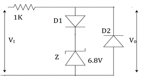
- a)6.1V,-0.7V
- b)0.7V,-7.5V
- c)7.5V,-0.7V
- d)7.5V,-7.5V
Correct answer is option 'C'. Can you explain this answer?
In the given limiter circuit, an input voltage Vi=10sin100πt is applied. Assume that the diode drop is 0.7V when it’s forward biased. The zener breakdown voltage is 6.8V.The maximum and minimum values of outputs voltage are _______
a)
6.1V,-0.7V
b)
0.7V,-7.5V
c)
7.5V,-0.7V
d)
7.5V,-7.5V
 | Ishani Chauhan answered |
With VI= 10V when maximum, D1 is forward biased, D2 is reverse biased. Zener is in breakdown region. VOMAX=sum of breakdown voltage and diode drop=6.8+0.7=7.5V. VOMIN=negative of voltage drop=-0.7V. There will be no breakdown voltage here.
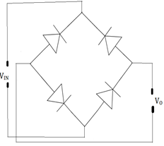
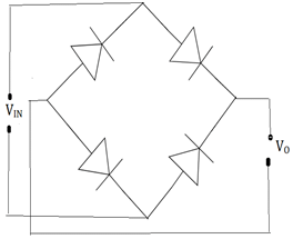
In the circuits given below, the correct full wave rectifier is _________- a)
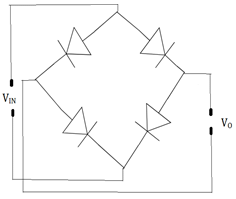
- b)
- c)
- d)
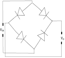
Correct answer is option 'C'. Can you explain this answer?
In the circuits given below, the correct full wave rectifier is _________
a)
b)
c)
d)
 | Rutuja Deshpande answered |
When the input is applied, a full wave rectifier should have a current flow. The flow should be in the same direction for both positive and negative half cycles. Only the third circuit satisfies the above condition.
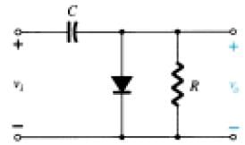
What is the circuit in the given diagram called?
- a)Clipper
- b)Clamper
- c)Half wave rectifier
- d)Full wave rectifier
Correct answer is option 'B'. Can you explain this answer?
What is the circuit in the given diagram called?
a)
Clipper
b)
Clamper
c)
Half wave rectifier
d)
Full wave rectifier
| | Sarita Yadav answered |
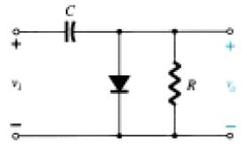
During the positive half cycle, the diode is forward biased and no signal appears across the output. The capacitor holds the charge in that state. During negative cycle, diode is reverse biased and diode does not conduct. The charge in capacitor is released and is obtained at the output.
When the regulation by a Zener diode is with a varying input voltage, what happens to the voltage drop across the resistance?- a)Decreases
- b)Has no effect on voltage
- c)Increases
- d)The variations depend on temperature
Correct answer is option 'C'. Can you explain this answer?
When the regulation by a Zener diode is with a varying input voltage, what happens to the voltage drop across the resistance?
a)
Decreases
b)
Has no effect on voltage
c)
Increases
d)
The variations depend on temperature
 | Bijoy Chauhan answered |
When the input voltage varies, the input current also varies. This makes more current to flow in the diode. This increase in the current should balance a change in the load current. Hence the voltage drop increases across the resistor.
For the given circuit, what is the minimum peak value of the output waveform if the input waveform is 10V square wave with switching time of 1 second?
Assume that the input switches between +10V and -10V DC levels.
- a)0 V
- b)-5 V
- c)-20 V
- d)-10 V
Correct answer is option 'C'. Can you explain this answer?
For the given circuit, what is the minimum peak value of the output waveform if the input waveform is 10V square wave with switching time of 1 second?
Assume that the input switches between +10V and -10V DC levels.
Assume that the input switches between +10V and -10V DC levels.
a)
0 V
b)
-5 V
c)
-20 V
d)
-10 V
| | Sarita Yadav answered |
For the positive half of the input, the diode is in the on state and hence acts as a short circuit and hence vo = 0 V. For the negative half cycle, the resistor receives voltage input both from the source and the capacitor which is charged during the positive half of the input. Hence, vo = -20 V.
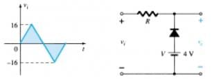
For a sinusoidal input of 20 Vpeak to the given circuit, what is the minimum value of the output waveform?
- a)20 V
- b)25 V
- c)-25 V
- d)0 V
Correct answer is option 'D'. Can you explain this answer?
For a sinusoidal input of 20 Vpeak to the given circuit, what is the minimum value of the output waveform?
a)
20 V
b)
25 V
c)
-25 V
d)
0 V
| | Ravi Singh answered |
The given circuit is a clipper that cuts off a part of the negative cycle of the input sinusoid i.e. the output becomes zero for a certain region of the input waveform. Hence, the minimum value is 0 V.
For the given input waveform to the given circuit, what is the peak value of the output waveform?
- a)0 V
- b)16 V
- c)12 V
- d)None of these
Correct answer is option 'B'. Can you explain this answer?
For the given input waveform to the given circuit, what is the peak value of the output waveform?
a)
0 V
b)
16 V
c)
12 V
d)
None of these
| | Yash Patel answered |
In the given circuit, the diode is in the off stage when vi > 4 V. Hence, when vi > 4 V, vo = vi and hence the peak value of vo = the peak value of vi = 16 V.
For the given input waveform to the given circuit, what is the minimum value of the output waveform?
- a)4 V
- b)16 V
- c)12 V
- d)0 V
Correct answer is option 'A'. Can you explain this answer?
For the given input waveform to the given circuit, what is the minimum value of the output waveform?
a)
4 V
b)
16 V
c)
12 V
d)
0 V
| | Sarita Yadav answered |
The circuit above is a parallel clipper. When the input is less than 4V, then diode is forward biased and thus output voltage is 4V. When input increases above 4V, the diode is reverse biased and output is equal to the input. Hence, minimum output is 4V.
In a centre tapped full wave rectifier, RL=1KΩ and for diode Rf=10Ω. The primary voltage is 800sinωt with transformer turns ratio=2. The ripple factor will be _________ 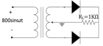
- a)54%
- b)48%
- c)26%
- d)81%
Correct answer is option 'B'. Can you explain this answer?
In a centre tapped full wave rectifier, RL=1KΩ and for diode Rf=10Ω. The primary voltage is 800sinωt with transformer turns ratio=2. The ripple factor will be _________
a)
54%
b)
48%
c)
26%
d)
81%
| | Charvi Kaur answered |
The ripple factor ϒ= [(IRMS/IAVG)2 – 1]1/2. IRMS =Im /√2=Vm/(Rf+RL)√2=200/1.01=198.
(Secondary line to line voltage is 800/2=400. Due to centre tap Vm=400/2=200)
IRMS=198/√2=140mA, IAVG=2*198/π=126mA. ϒ=[(140/126)2-1]1/2=0.48. So, ϒ=48%.
(Secondary line to line voltage is 800/2=400. Due to centre tap Vm=400/2=200)
IRMS=198/√2=140mA, IAVG=2*198/π=126mA. ϒ=[(140/126)2-1]1/2=0.48. So, ϒ=48%.
For the given circuit and input waveform, the peak value of the output is +30V.

- a)True
- b)False
- c)Value can not be determined
- d)None of the above
Correct answer is option 'A'. Can you explain this answer?
For the given circuit and input waveform, the peak value of the output is +30V.
a)
True
b)
False
c)
Value can not be determined
d)
None of the above
| | Ravi Singh answered |
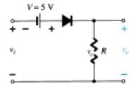
The given circuit is a clamper with an independent DC supply of +10 V. Keeping in mind the connection of the diode and the DC supply, we see that the output waveform is clamped at +10V i.e. it shifts up by +10V. Hence, the maximum value of vo = +30 V.
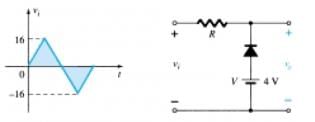
For a sinusoidal input of 20 Vpeak to the given circuit, what is the peak value of the output waveform?
- a)20 V
- b)25 V
- c)0 V
- d)-25 V
Correct answer is option 'B'. Can you explain this answer?
For a sinusoidal input of 20 Vpeak to the given circuit, what is the peak value of the output waveform?
a)
20 V
b)
25 V
c)
0 V
d)
-25 V
| | Ravi Singh answered |
In the given circuit, the output becomes zero for vi less than -5 V. Hence, the peak value of the output is 25 V owing to the additive effect of V for vi.
What is the output as a function of the input voltage (for positive values) for the given figure. Assume it’s an ideal op-amp with zero forward drop (Di=0)
- a)0
- b)-Vi
- c)Vi
- d) 2Vi
Correct answer is option 'C'. Can you explain this answer?
What is the output as a function of the input voltage (for positive values) for the given figure. Assume it’s an ideal op-amp with zero forward drop (Di=0)
a)
0
b)
-Vi
c)
Vi
d)
2Vi
| | Sarthak Yadav answered |
When the input of the inverted mode op-amp is positive, the output is negative.
The diode is reverse biased. The input appears at the output.
The diode is reverse biased. The input appears at the output.
Chapter doubts & questions for Simple Diode Circuits - Analog and Digital Electronics 2026 is part of Electrical Engineering (EE) exam preparation. The chapters have been prepared according to the Electrical Engineering (EE) exam syllabus. The Chapter doubts & questions, notes, tests & MCQs are made for Electrical Engineering (EE) 2026 Exam. Find important definitions, questions, notes, meanings, examples, exercises, MCQs and online tests here.
Chapter doubts & questions of Simple Diode Circuits - Analog and Digital Electronics in English & Hindi are available as part of Electrical Engineering (EE) exam. Download more important topics, notes, lectures and mock test series for Electrical Engineering (EE) Exam by signing up for free.
Analog and Digital Electronics135 videos|183 docs|71 tests |