


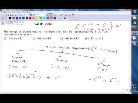
All Exams > Electrical Engineering (EE) > Digital Electronics > All Questions
All questions of Practice Tests: Digital Electronics for Electrical Engineering (EE) Exam
If Vin is 0.99 V, what is the digital output of the ADC 0801 after INTER goes low?- a)0011 0011
- b)0101 1111
- c)0111 1100
- d)1111 1111
Correct answer is option 'A'. Can you explain this answer?
If Vin is 0.99 V, what is the digital output of the ADC 0801 after INTER goes low?
a)
0011 0011
b)
0101 1111
c)
0111 1100
d)
1111 1111
| | Gitanjali Deshpande answered |
Given: Vin = 0.99 V
ADC0801 is an 8-bit analog to digital converter.
It has a resolution of 2^8 = 256 levels.
The input voltage range of the ADC is from 0 to 5 V.
The conversion formula for the ADC0801 is given as:
Digital output = (Vin / Vref) * 256
where Vref is the reference voltage, which is equal to 5 V for the ADC0801.
Calculating the digital output:
Digital output = (0.99 V / 5 V) * 256
= 50.664
The digital output is a binary number, so we need to convert the decimal number 50.664 to binary.
The integer part of the number is 50, which is equal to 0011 0010 in binary.
The fractional part of the number is 0.664. To convert this to binary, we can multiply it by 2 and take the integer part of the result. This gives:
0.664 * 2 = 1.328
integer part = 1
0.328 * 2 = 0.656
integer part = 0
0.656 * 2 = 1.312
integer part = 1
0.312 * 2 = 0.624
integer part = 0
and so on...
Continuing this process for 8 bits, we get:
0.664 * 2 = 1.328 --> 1
0.328 * 2 = 0.656 --> 0
0.656 * 2 = 1.312 --> 1
0.312 * 2 = 0.624 --> 0
0.624 * 2 = 1.248 --> 1
0.248 * 2 = 0.496 --> 0
0.496 * 2 = 0.992 --> 0
0.992 * 2 = 1.984 --> 1
So the final binary value is:
0011 0010.1010
However, the ADC0801 only outputs an 8-bit digital value, so we need to round the binary number to the nearest 8-bit value.
The 9th bit is a 1, so we round up to the next 8-bit value, which is:
0011 0011
Therefore, the digital output of the ADC0801 after INTER goes low is option 'A' - 0011 0011.

Which of the following is incorrect?- a)(8)16 = (8)8
- b)(5)16 = (5)8
- c)(8)2 = (2)10
- d)(2)16 = (2)10
Correct answer is option 'A'. Can you explain this answer?
Which of the following is incorrect?
a)
(8)16 = (8)8
b)
(5)16 = (5)8
c)
(8)2 = (2)10
d)
(2)16 = (2)10
 | Shanta B answered |
Since, (8)16=(10) 8 so option (a) is incorrect
and (8) 2 will be not possible so (c) also incorrect
and (8) 2 will be not possible so (c) also incorrect
In 8421 Binary coded Decimal system the decimal number 237 is represented by- a)1000110111
- b)1000111110
- c)001000110111
- d)10010010011
Correct answer is option 'C'. Can you explain this answer?
In 8421 Binary coded Decimal system the decimal number 237 is represented by
a)
1000110111
b)
1000111110
c)
001000110111
d)
10010010011
| | Ravi Singh answered |
Correct Answer :- c
Explanation : The decimal number is 2 3 7.
2 = 0010
3 = 0011
7 = 0111
The answer is correct C. 0010 0011 0111.
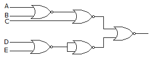
For the logic circuit of the given figure the simplified Boolean expression is
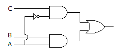
- a)
- b)
- c)Y = ABC
- d)
Correct answer is option 'A'. Can you explain this answer?
For the logic circuit of the given figure the simplified Boolean expression is
a)
b)
c)
Y = ABC
d)
 | Shanta B answered |
First gate a1=C.A'
second gate a2=A.B
Y=a1+a2=C.A'+A.B~>option(a)
second gate a2=A.B
Y=a1+a2=C.A'+A.B~>option(a)
Typical size of digital IC is about- a)1″ x 1″
- b)2″ x 2″
- c)0.1″ x 0.1″
- d)0.001″ x 0.001″
Correct answer is option 'C'. Can you explain this answer?
Typical size of digital IC is about
a)
1″ x 1″
b)
2″ x 2″
c)
0.1″ x 0.1″
d)
0.001″ x 0.001″
| | Prasad Saini answered |
Digital integrated circuits (ICs) are electronic components that contain thousands or millions of transistors, resistors, and capacitors fabricated on a small semiconductor wafer. These ICs are widely used in various electronic devices, such as computers, smartphones, and digital appliances, to perform complex functions.
The typical size of a digital IC is about 0.1" x 0.1", which corresponds to approximately 2.54 mm x 2.54 mm. This size is considered standard for most digital ICs, but it can vary depending on the complexity and functionality of the circuit.
Explanation:
1. Definition of Digital IC:
- Digital integrated circuits are electronic components that consist of interconnected electronic devices and passive components on a semiconductor wafer.
2. Size of Digital IC:
- The size of a digital IC refers to the dimensions of its physical package or chip.
- The typical size of a digital IC is about 0.1" x 0.1", which is equivalent to approximately 2.54 mm x 2.54 mm.
- This size is commonly referred to as a "chip" or "die" size.
3. Factors affecting IC size:
- The size of a digital IC depends on various factors, including the complexity of the circuit, the number of transistors, the required functionality, and the manufacturing process technology.
- As technology advances, the size of digital ICs tends to decrease due to the ability to fabricate smaller transistors and integrate more components on a single chip.
4. Miniaturization of ICs:
- The miniaturization of ICs has been a significant trend in the semiconductor industry, driven by the need for smaller, faster, and more power-efficient electronic devices.
- Smaller ICs allow for higher packing densities, which enable the integration of more functionality in a smaller form factor.
5. Advantages of smaller IC size:
- Smaller ICs offer several advantages, such as reduced power consumption, faster signal propagation, improved thermal performance, and cost savings due to higher yield rates during manufacturing.
6. Application of Digital ICs:
- Digital ICs are widely used in various applications, including microprocessors, memory chips, digital signal processors, programmable logic devices, and application-specific integrated circuits (ASICs).
- These ICs enable the execution of complex digital functions, such as arithmetic operations, data storage, logic operations, and communication protocols.
In conclusion, the typical size of a digital IC is about 0.1" x 0.1" (2.54 mm x 2.54 mm), which is the standard size for most digital ICs. However, it's important to note that IC sizes can vary depending on the complexity and functionality of the circuit, as well as advancements in semiconductor manufacturing technology.
The logic circuit of the given figure realizes the function
- a)
- b)
- c)
- d)
Correct answer is option 'A'. Can you explain this answer?
The logic circuit of the given figure realizes the function
a)
b)
c)
d)
 | Rohit Raj answered |
Kindly check the question again.
Which of the following is incorrect?- a)11101 + 10 = 11111
- b)(8)8 + (2)8 = (11)8
- c)(8)16 + (7)16 = E
- d)All of them are incorrect
Correct answer is option 'B'. Can you explain this answer?
Which of the following is incorrect?
a)
11101 + 10 = 11111
b)
(8)8 + (2)8 = (11)8
c)
(8)16 + (7)16 = E
d)
All of them are incorrect
| | Anoushka Kumar answered |
Understanding the Given Options
To determine which of the options is incorrect, we need to evaluate each equation carefully.
Option A: 11101 + 10 = 11111
- This is a binary addition.
- 11101 (which is 29 in decimal) + 10 (which is 2 in decimal) equals 11111 (which is 31 in decimal).
- Therefore, this option is correct.
Option B: (8)8 + (2)8 = (11)8
- This is an octal addition.
- (8)8 is not a valid octal number because octal digits only range from 0 to 7.
- Therefore, this option is incorrect.
Option C: (8)16 + (7)16 = E
- This is a hexadecimal addition.
- (8)16 is 8 in decimal, and (7)16 is 7 in decimal.
- Adding these gives us 15 in decimal, which is represented as F in hexadecimal, not E.
- Therefore, this option is also incorrect.
Conclusion
- While option B is indeed incorrect due to the invalid octal digit, option C is also incorrect for a different reason. Thus, the correct answer is that both B and C are incorrect, making option D (all are incorrect) the most precise answer.
In summary, the evaluation highlights that option B is incorrect because (8)8 is not a valid octal number, while option C is incorrect due to a misrepresentation in hexadecimal addition.
Suppose a microprocessor has memory locations from 0000 to 3FFF, each storing I byte. How many bytes the memory can storing I bytes the memory can store?- a)4384
- b)8644
- c)12688
- d)16384
Correct answer is option 'B'. Can you explain this answer?
Suppose a microprocessor has memory locations from 0000 to 3FFF, each storing I byte. How many bytes the memory can storing I bytes the memory can store?
a)
4384
b)
8644
c)
12688
d)
16384
 | Rozy Jha answered |
Correct answer should be (d) : 16384
as the no. of bits in 3FFF is 14 therefore total no. of memory location can be connected is 2^14 i.e. 16384
as the no. of bits in 3FFF is 14 therefore total no. of memory location can be connected is 2^14 i.e. 16384
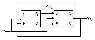
In the circuit shown below, the outputs Y1 and Y2 for the given initial condition Y1 = Y2 = 1 and after four input pulses will be
- a)Y1 = 1, Y2 = 0
- b)Y1 = 0, Y2 = 0
- c)Y1 = 0, Y2 = 1
- d)Y1 = 1, Y2 = 1
Correct answer is option 'D'. Can you explain this answer?
In the circuit shown below, the outputs Y1 and Y2 for the given initial condition Y1 = Y2 = 1 and after four input pulses will be
a)
Y1 = 1, Y2 = 0
b)
Y1 = 0, Y2 = 0
c)
Y1 = 0, Y2 = 1
d)
Y1 = 1, Y2 = 1
| | Shanta B answered |
From given data,
first flip-flop, j=0 (since, y2=Q=1 so Q'=0) and k=1(since, y2=1)
therefore, y1=Q=0
second flip-flop, j=0 (since, y1=Q=0) and k=1(since,y1=Q=0 so Q'=1)
therefore, y2=Q=0
for next round,
first flip-flop, j=1 (since, y2=Q=0 so Q'=1) and k=0(since, y2=0)
therefore, y1=Q=1
second flip-flop, j=1 (since, y1=Q=1) and k=0(since,y1=Q=1 so Q'=0)
therefore, y2=Q=1
and it repeats
so for odd rounds output is y1=y2=0
and for even rounds output is y1=y2=1
In a positive-edge-triggered JK flip-flop, a low J and a low K produce __________ state. A high __________ on the rising edge of the clock.- a)inactive, reset
- b)active, reset
- c)active, toggle
- d)inactive, toggle
Correct answer is option 'D'. Can you explain this answer?
In a positive-edge-triggered JK flip-flop, a low J and a low K produce __________ state. A high __________ on the rising edge of the clock.
a)
inactive, reset
b)
active, reset
c)
active, toggle
d)
inactive, toggle
| | Ishan Saini answered |
**Positive-Edge-Triggered JK Flip-Flop**
A positive-edge-triggered JK flip-flop is a type of sequential logic circuit that stores and outputs a single bit of information. It is called positive-edge-triggered because it only responds to changes in the input signals when the clock signal transitions from low to high (i.e., rising edge).
**JK Flip-Flop Truth Table**
The truth table for a positive-edge-triggered JK flip-flop is as follows:
```
Clock (CLK) J K Q(t) Q(t+1)
-----------------------------------
0 X X Q Q
1 0 0 Q Q
1 0 1 Q 0
1 1 0 Q 1
1 1 1 Q ~Q
```
Where:
- CLK represents the clock input
- J represents the J input
- K represents the K input
- Q(t) represents the current state of the flip-flop output
- Q(t+1) represents the next state of the flip-flop output
**Effect of Low J and Low K Inputs**
When both J and K inputs of a positive-edge-triggered JK flip-flop are low, the flip-flop enters an inactive state. This means that the output state (Q) remains unchanged regardless of the clock signal.
- When CLK = 0 (low), the output (Q) remains the same as the previous state.
- When CLK = 1 (rising edge), the output (Q) remains the same as the previous state.
**Effect of High J and Low K Inputs on Rising Edge of Clock**
When the J input is high and the K input is low, the flip-flop enters a toggle state. This means that the output state (Q) toggles between 1 and 0 on the rising edge of the clock.
- When CLK = 0 (low), the output (Q) remains the same as the previous state.
- When CLK = 1 (rising edge), the output (Q) toggles between 1 and 0. If the previous state was 1, the next state will be 0. If the previous state was 0, the next state will be 1.
Therefore, the correct answer is option D: Inactive state for low J and low K inputs, and toggle state for high J and low K inputs on the rising edge of the clock.
How many interrupts are there of 8085 μP?- a)4
- b)5
- c)6
- d)8
Correct answer is option 'B'. Can you explain this answer?
How many interrupts are there of 8085 μP?
a)
4
b)
5
c)
6
d)
8
| | Rohit Raj answered |
INTR, RST 5.5, RST 6.5, RST 7.5 are maskable interrupts and TRAP is an only non-maskable interrupt
The rate of change of digital signals between High and Low level is- a)very fast
- b)fast
- c)slow
- d)very slow
Correct answer is option 'A'. Can you explain this answer?
The rate of change of digital signals between High and Low level is
a)
very fast
b)
fast
c)
slow
d)
very slow
| | Sandeep Chatterjee answered |
Introduction:
In the realm of digital communication, signals are used to transmit information. These signals can be in the form of electrical voltages that represent different states, such as high and low levels. The rate at which these signals change from a high level to a low level or vice versa is an important factor in determining the efficiency and reliability of the communication system.
The rate of change of digital signals:
The rate of change of digital signals refers to the speed at which the signals transition from a high level to a low level or vice versa. This rate of change is commonly measured in terms of the rise time and fall time of the signal. The rise time is the time it takes for the signal to transition from a low level to a high level, while the fall time is the time it takes for the signal to transition from a high level to a low level.
Explanation of the correct answer:
The correct answer to the question is option 'A' - very fast. This means that the rate of change of digital signals between high and low levels is very rapid.
Reasoning:
The rate of change of digital signals is typically very fast due to several reasons:
1. Switching speed of electronic devices:
Digital signals are usually generated and processed by electronic devices such as transistors, integrated circuits, and microprocessors. These devices are designed to switch between high and low levels at very high speeds, often in the range of nanoseconds or picoseconds. The fast switching speed of these devices allows for rapid transitions between high and low levels, resulting in a high rate of change of the digital signals.
2. Bandwidth considerations:
In digital communication systems, the bandwidth available for transmitting signals is limited. To maximize the utilization of the available bandwidth, it is desirable to transmit as many digital signal transitions as possible within a given time period. This requires the rate of change of the digital signals to be very fast.
3. Minimizing signal distortion:
Digital signals are susceptible to various forms of distortion during transmission, such as noise, interference, and attenuation. Fast signal transitions help to minimize the impact of these distortions by reducing the time during which the signal is vulnerable to external influences. This enhances the overall signal quality and reliability.
Conclusion:
In conclusion, the rate of change of digital signals between high and low levels is very fast. This fast rate of change is essential for efficient and reliable digital communication, enabling high-speed switching, maximizing bandwidth utilization, and minimizing signal distortion.
In 8085 microprocessor, if interrupt service requests have been received from all of the following interrupts, then which one will be serviced first?- a)RST 5.5
- b)RST 6.5
- c)RST 7.5
- d)None
Correct answer is option 'C'. Can you explain this answer?
In 8085 microprocessor, if interrupt service requests have been received from all of the following interrupts, then which one will be serviced first?
a)
RST 5.5
b)
RST 6.5
c)
RST 7.5
d)
None
 | Aashwin Trivedi answered |
There is no big concept only theory you need to know that the sequence of order of interrupts
hold>intr>rst7.5>rst6.5>rst5.5
hold>intr>rst7.5>rst6.5>rst5.5
Which of them radiates emission?- a)LED only
- b)LCD only
- c)Both LED and LCD
- d)Neither LED nor LCD
Correct answer is option 'A'. Can you explain this answer?
Which of them radiates emission?
a)
LED only
b)
LCD only
c)
Both LED and LCD
d)
Neither LED nor LCD
| | Rajveer Saha answered |
Answer:
LEDs (Light Emitting Diodes) are the only ones that radiate emissions.
Explanation:
LED stands for Light Emitting Diode, which is a semiconductor device that emits light when an electric current is applied to it. On the other hand, LCD stands for Liquid Crystal Display, which is a type of flat panel display that uses liquid crystals to produce images.
LED emits light while LCD uses a backlight to illuminate the screen. Therefore, LEDs are the only ones that radiate emissions.
Summary:
- LED emits light when an electric current is applied to it.
- LCD uses a backlight to illuminate the screen.
- LEDs are the only ones that radiate emissions.
When two 16-input multiplexers drive a 2-input MUX, what is the result?- a)2-input MUX
- b)4-input MUX
- c)16-input MUX
- d)32 input MUX
Correct answer is option 'D'. Can you explain this answer?
When two 16-input multiplexers drive a 2-input MUX, what is the result?
a)
2-input MUX
b)
4-input MUX
c)
16-input MUX
d)
32 input MUX
| | Avantika Kaur answered |
Explanation:
When two 16-input multiplexers drive a 2-input MUX, the result is a 32-input MUX. This can be explained as follows:
Working of Multiplexers:
A multiplexer (MUX) is a device that selects one of several input signals and forwards the selected input into a single output line. It is also known as a data selector. A multiplexer has two sets of inputs: data inputs and control inputs. The data inputs are the signals to be selected, and the control inputs determine which data input is selected.
A 2-input MUX has two data inputs (D0 and D1), one select input (S), and one output (Y). The output is connected to either D0 or D1 depending on the value of the select input (S). If S=0, then D0 is selected, and if S=1, then D1 is selected.
Similarly, a 16-input MUX has sixteen data inputs (D0 to D15), four select inputs (S0 to S3), and one output (Y). The output is connected to one of the sixteen data inputs depending on the values of the select inputs.
Working of 32-input MUX:
When two 16-input MUXes drive a 2-input MUX, the 16 inputs of each 16-input MUX are connected to the 16 data inputs of the 2-input MUX. The select inputs of the two 16-input MUXes are connected to the two data inputs of the 2-input MUX.
This configuration forms a 32-input MUX with two sets of select inputs (S0 and S1) and one output (Y). The output is connected to one of the thirty-two data inputs depending on the values of the select inputs.
Conclusion:
Thus, the result of two 16-input MUXes driving a 2-input MUX is a 32-input MUX.
Which of the following is best suited for parity checking and parity generation?- a)AND, OR, NOT gates
- b)XOR, Exclusive NOR gate
- c)NAND gates
- d)NOR gates
Correct answer is option 'B'. Can you explain this answer?
Which of the following is best suited for parity checking and parity generation?
a)
AND, OR, NOT gates
b)
XOR, Exclusive NOR gate
c)
NAND gates
d)
NOR gates
| | Shanta B answered |
Parity check : EXOR
parity generation : EXNOR
Explanation
Parity generation
The XNOR gate will emit 1 only when there is not exactly one 1 input.
This feature can be used for parity generation.
Suppose A wants to send 1001. XNOR gate will give parity as 0.
But if A sends 1000 XNOR gate gives 1 as parity
Parity check
B receives: 10010
B computes parity: 1+0+0+1+0 (mod 2) = 0 //this can be achieved by EXOR
For a particular type of memory the access time and cycle time are 200 ns each. The maximum rate at which data can be accessed by- a)2.5 x 10⁶/s
- b)5 x 10⁶/s
- c)0.2 x l06/s
- d)106/s
Correct answer is option 'A'. Can you explain this answer?
For a particular type of memory the access time and cycle time are 200 ns each. The maximum rate at which data can be accessed by
a)
2.5 x 10⁶/s
b)
5 x 10⁶/s
c)
0.2 x l06/s
d)
106/s
| | Mihir Khanna answered |
Memory Access Time and Cycle Time
Memory access time is the time required to read or write data to memory, while cycle time is the time between consecutive memory operations. In a particular type of memory, both the access time and cycle time are 200 ns.
Maximum Data Access Rate
The maximum data access rate is the maximum amount of data that can be accessed per second. It is calculated as the reciprocal of the cycle time, i.e., 1/cycle time. Therefore, the maximum data access rate for this memory is:
Maximum data access rate = 1/cycle time = 1/200 ns = 5 x 10⁶/s
Answer
Option 'A' is the correct answer, which is 2.5 x 10⁶/s. This is because the maximum data access rate is usually half of the maximum clock frequency. In this case, the clock frequency is 1/cycle time, which is 5 MHz. Therefore, the maximum data access rate is half of 5 MHz, which is 2.5 x 10⁶/s.
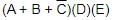
The Boolean expression (A+ B) (A +C) (B+C) simplifies to- a)(A + B)C
- b)(A +B)C
- c)(A+ B)C
- d)none of these
Correct answer is 'C'. Can you explain this answer?
The Boolean expression (
A
+ B) (A +C
) (B
+C
) simplifies toa)
(A + B)
C
b)
(A +
B
)C
c)
(
A
+ B)C
d)
none of these
| | Rithika Pillai answered |
Given,
Period = 4 x Pulse width
Duty cycle is the fraction of time the signal is high (or low) compared to the total time period.
Let's assume the pulse width as 't' and the period as '4t'.
Calculation:
Total time period = Pulse width + Off time
4t = t + Off time
Off time = 3t
Duty cycle = (Pulse width / Total time period) x 100%
= (t / (t + 3t)) x 100%
= (t / 4t) x 100%
= 25%
Therefore, the duty cycle of the waveform is 25%.
The principal of locality of reference justifies the use of- a)interrupts
- b)DMA
- c)virtual memory
- d)cache memory
Correct answer is option 'D'. Can you explain this answer?
The principal of locality of reference justifies the use of
a)
interrupts
b)
DMA
c)
virtual memory
d)
cache memory
| | Debanshi Basak answered |
Principal of Locality of Reference:
The principal of locality of reference is a fundamental concept in computer science and refers to the tendency of a program to access data and instructions that are close to each other in both time and space. It states that programs tend to access a relatively small portion of their address space at any given time, and that this portion changes over time.
Cache Memory:
Cache memory is a small, fast memory that is used to store frequently accessed data or instructions. It acts as a buffer between the central processing unit (CPU) and the main memory, providing faster access to the data that is needed by the CPU. Cache memory operates on the principle of locality of reference, exploiting the fact that programs tend to access the same data or instructions repeatedly.
Explanation:
Cache memory is justified by the principal of locality of reference because it takes advantage of the fact that programs frequently access the same data or instructions. This is achieved through two main types of locality: temporal locality and spatial locality.
Temporal locality:
Temporal locality refers to the tendency of a program to access the same data or instructions repeatedly over a short period of time. Cache memory exploits temporal locality by storing recently accessed data or instructions in a small, fast memory. This reduces the time it takes to access the data or instructions, as they can be retrieved from the cache instead of the slower main memory.
Spatial locality:
Spatial locality refers to the tendency of a program to access data or instructions that are close to each other in memory. Cache memory exploits spatial locality by storing not only the requested data or instructions, but also a portion of the surrounding data or instructions. This increases the likelihood that future accesses will be satisfied by the cache, further reducing access time.
Benefits of Cache Memory:
- Faster access time: Cache memory allows for quicker access to frequently accessed data or instructions, reducing the overall execution time of a program.
- Reduced memory traffic: By storing frequently accessed data or instructions in cache, the need to fetch them from the main memory is reduced, resulting in less memory traffic.
- Improved performance: Cache memory improves the overall performance of a computer system by reducing memory latency and increasing the effective memory bandwidth.
Given the principal of locality of reference, cache memory is a crucial component in modern computer systems as it effectively utilizes the concept of temporal and spatial locality to provide faster access to frequently accessed data or instructions.
If we need a low noise device, we should use- a)BJT
- b)FET
- c)thyristor
- d)UJT
Correct answer is option 'B'. Can you explain this answer?
If we need a low noise device, we should use
a)
BJT
b)
FET
c)
thyristor
d)
UJT
| | Kajal Mukherjee answered |
Low Noise Device: FET
FETs (Field Effect Transistors) are considered low noise devices as they have a higher input impedance than BJT (Bipolar Junction Transistors) and are less sensitive to temperature changes. This makes them ideal for applications where low noise is important, such as in amplifiers, mixers, and oscillators.
Why FET is a low noise device?
1. Higher input impedance: FETs have a high input impedance due to the absence of a base current in the device. This leads to a lower noise figure as the input signal is not affected by the noise generated by the input circuit.
2. Less sensitive to temperature changes: FETs are less sensitive to temperature changes as the channel resistance is stable over a wide temperature range. This leads to a more stable device with less noise generated by the device itself.
3. Lower flicker noise: FETs have lower flicker noise compared to BJT as the noise generated by the device decreases as the frequency increases. This makes FETs ideal for low-frequency applications where flicker noise can be a problem.
Conclusion
In conclusion, FETs are a better choice when low noise is important as they have a higher input impedance, are less sensitive to temperature changes, and have lower flicker noise compared to BJT.
Assuming accumulator contain A 64 and the carry is set (1). What will accumulator (A) and carry (CY) contain after ANA A?- a)A 6 H, 1
- b)A 6 H, 0
- c)00 H, 0
- d)00 H, 1
Correct answer is option 'B'. Can you explain this answer?
Assuming accumulator contain A 64 and the carry is set (1). What will accumulator (A) and carry (CY) contain after ANA A?
a)
A 6 H, 1
b)
A 6 H, 0
c)
00 H, 0
d)
00 H, 1
| | Sparsh Nambiar answered |
Answer:
Assuming accumulator contain A 64 and the carry is set (1). What will accumulator (A) and carry (CY) contain after ANA A?
The ANA instruction performs a bitwise logical AND operation between the contents of the accumulator and the operand, which can be a register or a memory location. The result of the operation is stored in the accumulator, and the carry flag is updated based on the result.
Given that the accumulator contains A 64 and the carry flag is set, the ANA operation will perform a logical AND between the accumulator and itself, which is equivalent to performing a bitwise complement of the accumulator. The carry flag is set, so the result will be affected by the carry flag.
The possible outcomes of the operation are:
A) A 6 H, 1: This is not correct because the ANA operation should not affect the carry flag. The result of the operation is A AND A, which is equal to A, so the contents of the accumulator should not change.
B) A 6 H, 0: This is the correct answer. The ANA operation should set the carry flag to 0 because the result of A AND A with carry is equal to A, and A does not have any bit set to 1 that could generate a carry. Therefore, the contents of the accumulator remain unchanged, and the carry flag is updated to 0.
C) 00 H, 0: This is not correct because the ANA operation should not clear the accumulator. The result of A AND A with carry is equal to A, so the contents of the accumulator should not change.
D) 00 H, 1: This is not correct because the ANA operation should not set the carry flag. The result of A AND A with carry is equal to A, so the carry flag should be updated to 0.
Therefore, the correct answer is B) A 6 H, 0.
In 1-to-4 demultiplexer, how many select lines are required?- a)2
- b)3
- c)4
- d)5
Correct answer is option 'A'. Can you explain this answer?
In 1-to-4 demultiplexer, how many select lines are required?
a)
2
b)
3
c)
4
d)
5
| | Mansi Choudhury answered |
1-to-4 Demultiplexer
In a digital circuit, a demultiplexer (or demux) is a combinational logic circuit that takes a single input and selects one of many possible outputs based on the value of select lines. A 1-to-4 demultiplexer has one input line and four output lines.
Select Lines
The select lines in a demultiplexer determine which output line is selected. In a 1-to-4 demultiplexer, the number of select lines required can be calculated using the formula 2^n = m, where n is the number of select lines and m is the number of output lines.
In this case, we have 4 output lines. Therefore, to find the number of select lines required, we need to solve the equation 2^n = 4.
Solving for n
To find the value of n, we can use trial and error. Starting with n = 1, we can substitute the value of n into the equation and check if 2^n equals 4.
- For n = 1, 2^1 = 2 (not equal to 4)
- For n = 2, 2^2 = 4 (equal to 4)
Therefore, the number of select lines required for a 1-to-4 demultiplexer is 2 (option A).
Explanation
A 1-to-4 demultiplexer has one input line and four output lines. The select lines determine which output line is selected. The number of select lines required can be found using the formula 2^n = m, where n is the number of select lines and m is the number of output lines.
In this case, we have 4 output lines. By solving the equation 2^n = 4, we find that n = 2. Therefore, 2 select lines are required for a 1-to-4 demultiplexer.
A microcomputer has memory locations from 0000 to FFFF, each storing 1 byte. How many bytes can be the memory store?- a)12333
- b)14666
- c)16384
- d)16655
Correct answer is option 'C'. Can you explain this answer?
A microcomputer has memory locations from 0000 to FFFF, each storing 1 byte. How many bytes can be the memory store?
a)
12333
b)
14666
c)
16384
d)
16655
| | Avik Saha answered |
Understanding Memory Locations
In a microcomputer, memory locations are typically represented in hexadecimal format. The address range from 0000 to FFFF denotes the total number of available memory addresses.
Total Address Calculation
- The range 0000 to FFFF includes:
- The first address: 0000 (in decimal, 0)
- The last address: FFFF (in decimal, 65535)
- To determine the total number of addresses:
- Total addresses = Last address - First address + 1
- Total addresses = 65535 - 0 + 1 = 65536
Memory Size in Bytes
- Each memory location can store 1 byte.
- Therefore, the total memory size in bytes is equal to the total number of addresses:
- Total memory size = 65536 bytes
Converting to Kilobytes
- To convert bytes to kilobytes (KB):
- Total memory size in KB = Total memory size in bytes / 1024
- Total memory size in KB = 65536 / 1024 = 64 KB
Conclusion
- The total number of bytes that can be stored in this memory range is 65536 bytes.
- This corresponds to 64 KB, which aligns with option 'C' being the correct answer, representing a total of 16384 memory locations, with each location storing 1 byte.
In summary, the microcomputer can store 65536 bytes, confirming that option C is indeed the right choice.
Find the decimal value of 1110012 :- a)5710
- b)5610
- c)4710
- d)3710
Correct answer is option 'A'. Can you explain this answer?
Find the decimal value of 1110012 :
a)
5710
b)
5610
c)
4710
d)
3710
| | Sahana Sarkar answered |
**Decimal Conversion of 1110012**
To convert a binary number to its decimal equivalent, we need to understand the place value system of binary numbers.
In binary representation, each digit can have one of two values: 0 or 1. The rightmost digit represents the unit's place, the next digit represents the two's place, the next digit represents the four's place, and so on.
Therefore, the decimal value of a binary number is calculated by multiplying each digit with its corresponding place value and adding them all together.
**Step-by-Step Calculation:**
1. Start from the rightmost digit (the unit's place) and assign the corresponding place value: 20 = 1.
2. Move to the next digit (the two's place) and assign the corresponding place value: 21 = 2.
3. Continue this process for each digit, assigning the corresponding place value: 22 = 4, 23 = 8, 24 = 16, 25 = 32.
4. Multiply each digit by its corresponding place value:
- 1 × 1 = 1
- 1 × 2 = 2
- 1 × 4 = 4
- 0 × 8 = 0
- 0 × 16 = 0
- 1 × 32 = 32
5. Add all the products together: 1 + 2 + 4 + 0 + 0 + 32 = 39.
Therefore, the decimal value of 1110012 is 39.
**Answer:**
The correct option is (a) 5710.
A digital clock uses __________ chip- a)SSI
- b)LSI
- c)VLSI
- d)MSI
Correct answer is option 'B'. Can you explain this answer?
A digital clock uses __________ chip
a)
SSI
b)
LSI
c)
VLSI
d)
MSI
 | Anirban Khanna answered |
Large-scale integration (LSI) is the process of integrating or embedding thousands of transistors on a single silicon semiconductor microchip. LSI technology was conceived in the mid-1970s when computer processor microchips were under development.
The contents of stack location 2109 H after the call operation will be
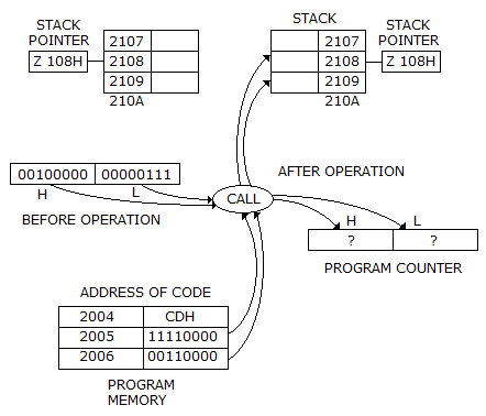
- a)00001111
- b)01010101
- c)00100000
- d)00100010
Correct answer is option 'C'. Can you explain this answer?
The contents of stack location 2109 H after the call operation will be
a)
00001111
b)
01010101
c)
00100000
d)
00100010
 | EduRev GATE answered |
Option C is correct.
The return address pushed on the stack by a CALL is the address of the instruction immediately following the CALL. The CALL at 2004H occupies 3 bytes, so the return address is 2007H.
Split 2007H into bytes: high-order = 20H → 00100000; low-order = 07H → 00000111.
The CALL pushes the return address bytes onto the stack; with the given stack layout these bytes appear at 2109H (high-order) and 2108H (low-order). Therefore 2109H = 00100000, i.e., option C.
The number of LED display indicators in logic probe are- a)1
- b)2
- c)1 or 2
- d)4
Correct answer is option 'B'. Can you explain this answer?
The number of LED display indicators in logic probe are
a)
1
b)
2
c)
1 or 2
d)
4
| | Sanchita Choudhary answered |
Logic Probe and LED Display Indicators
Introduction: A logic probe is an electronic test tool used to measure and analyze the behavior of digital circuits. It is used to detect and diagnose faults in digital circuits. The logic probe consists of a probe tip, a ground clip, and a handle. The probe tip is used to touch the test points of the circuit, and the ground clip is used to connect the probe to the ground of the circuit.
LED Display Indicators: LED display indicators are used on the logic probe to indicate the logic state of the circuit. The LED display indicators light up to indicate whether the circuit is in a high or low logic state. The LED display indicators are connected to the probe tip and ground clip.
Number of LED Display Indicators: The number of LED display indicators in the logic probe depends on the design of the probe. Some logic probes have one LED display indicator, while others have two or four LED display indicators.
Correct Answer: The correct answer to the question is option 'B', which states that there are two LED display indicators in the logic probe.
Explanation: The logic probe has two LED display indicators, one for the high logic state and one for the low logic state. The LED display indicators are connected to the probe tip and ground clip. When the probe tip touches a high logic state point in the circuit, the high LED display indicator lights up. When the probe tip touches a low logic state point in the circuit, the low LED display indicator lights up. The two LED display indicators help to provide a clear indication of the logic state of the circuit.
Which of the following circuits can be used as parallel-to-series converter?- a)Digital counter
- b)Decoder
- c)Demultiplexer
- d)Multiplexer
Correct answer is option 'D'. Can you explain this answer?
Which of the following circuits can be used as parallel-to-series converter?
a)
Digital counter
b)
Decoder
c)
Demultiplexer
d)
Multiplexer
| | Ayush Kumar answered |
Parallel-to-Series Converter:
A parallel-to-series converter, also known as a multiplexer or mux, is a digital circuit that combines multiple parallel input signals into a single serial output signal. It is commonly used in data communication systems, where it allows multiple data sources to share a single transmission line.
Multiplexer:
A multiplexer is a combinational logic circuit that selects one of many input lines and forwards it to a single output line. It has two types of inputs: data inputs and control inputs. The control inputs are used to select which data input is to be transmitted to the output.
Working Principle:
The multiplexer has 2^n data inputs and n control inputs, where n is the number of bits required to select one of the data inputs. The control inputs determine which data input is connected to the output.
The output of the multiplexer is a combination of the selected data input and the control inputs. The selected data input is transmitted to the output, while the remaining data inputs are disconnected.
Parallel-to-Series Conversion:
To convert parallel data to serial data using a multiplexer, each parallel input is connected to one of the data inputs of the multiplexer. The control inputs of the multiplexer are used to sequentially select each parallel input, transmitting them one by one to the output.
The control inputs can be generated using a counter, which counts from 0 to (2^n)-1, where n is the number of parallel inputs. The counter generates the control inputs in a sequential manner, allowing each parallel input to be transmitted to the output one at a time.
Answer: Multiplexer (Option D)
A multiplexer can be used as a parallel-to-series converter by connecting each parallel input to one of the data inputs of the multiplexer. The control inputs of the multiplexer can be generated using a digital counter, which sequentially selects each parallel input and transmits them to the output.
Option D, the multiplexer, is the correct answer as it is the only circuit among the given options that can be used as a parallel-to-series converter. The digital counter (option A) can be used to generate the control inputs for the multiplexer, but it is not a conversion circuit itself. The decoder (option B) and the demultiplexer (option C) are not suitable for parallel-to-series conversion as they are designed for different purposes.
Is Schottky TTL, Schottky diode is used primary to- a)prevent saturation of the transistor
- b)saturate the transistor
- c)act as a switch
- d)act as a controlling switch
Correct answer is option 'A'. Can you explain this answer?
Is Schottky TTL, Schottky diode is used primary to
a)
prevent saturation of the transistor
b)
saturate the transistor
c)
act as a switch
d)
act as a controlling switch
| | Jayant Mishra answered |
When forward biased, a Schottky diode's voltage drop is much less than a standard silicon diode's, 0.25 V versus 0.6 V. In a standard saturated transistor, the base-to-collector voltage is 0.6 V. In a Schottky transistor, the Schottky diode shunts current from the base into the collector before the transistor goes into.
As access time is decreased, the cost of memory- a)remains the same
- b)increases
- c)decreases
- d)may increase or decrease
Correct answer is option 'B'. Can you explain this answer?
As access time is decreased, the cost of memory
a)
remains the same
b)
increases
c)
decreases
d)
may increase or decrease
| | Palak Verma answered |
Explanation:
Access time refers to the time it takes to retrieve data from memory. In general, access time is inversely proportional to the cost of memory. As access time decreases, the cost of memory increases.
Reason:
Access time is a critical factor in determining the performance of a computer system. Faster access time allows for quicker data retrieval, resulting in improved system performance. However, achieving faster access time often requires the use of more advanced and expensive memory technologies.
Impact of faster access time on memory cost:
- Increased complexity: Achieving faster access time typically involves the use of more advanced memory technologies, such as faster integrated circuits or higher clock speeds. These advancements often come with increased complexity in design and manufacturing, which can drive up the cost of memory.
- Reduced production volume: Memory technologies with faster access times are often newer and less widely adopted compared to slower memory technologies. This typically leads to lower production volumes and higher manufacturing costs, further increasing the cost of memory.
- Higher demand: Faster access time is desirable for many applications, especially those requiring real-time data processing or high-performance computing. The increased demand for memory with faster access time can drive up prices due to supply and demand dynamics.
- R&D investments: Developing memory technologies with faster access times requires significant research and development investments. These investments need to be recovered through higher prices for the resulting memory products.
Therefore, as access time is decreased and faster memory technologies are used, the cost of memory increases. This relationship is commonly observed in the market, where memory modules with faster access times are typically priced higher than their slower counterparts.
What is the direction of control bus?- a)Unidirection into μp
- b)Unidirection out of up
- c)Bidirectional
- d)Mixed direction i.e., some lines into μp and some other out of μp
Correct answer is 'D'. Can you explain this answer?
What is the direction of control bus?
a)
Unidirection into μp
b)
Unidirection out of up
c)
Bidirectional
d)
Mixed direction i.e., some lines into μp and some other out of μp
| | Suyash Joshi answered |
Direction of Control Bus
The control bus is a collection of lines that are used to transmit control signals between the microprocessor and other components of the computer system. The direction of the control bus lines depends on their function and the type of device they are connecting to.
Bidirectional Control Bus
Some control bus lines are bidirectional, meaning they can transmit signals in both directions. These lines are used for communication between the microprocessor and other devices in the system, such as memory or input/output (I/O) devices. Examples of bidirectional control bus lines include:
- Data Bus: This line is used to transmit data between the microprocessor and other devices in the system.
- Address Bus: This line is used to transmit memory addresses from the microprocessor to memory devices.
- Control Bus: This line is used to transmit control signals between the microprocessor and other devices in the system, such as the interrupt request (IRQ) line or the read/write (R/W) line.
Mixed Direction Control Bus
Some control bus lines have mixed direction, meaning they can transmit signals in different directions depending on their function. These lines are used for communication between the microprocessor and other devices in the system, such as memory or I/O devices. Examples of mixed direction control bus lines include:
- Status Bus: This line is used to transmit status signals between the microprocessor and other devices in the system. Some status signals may be transmitted from the device to the microprocessor, while others may be transmitted from the microprocessor to the device.
- Clock Bus: This line is used to transmit clock signals between the microprocessor and other devices in the system. The clock signal may be generated by the microprocessor or by an external clock source.
Conclusion
In summary, the direction of the control bus lines depends on their function and the type of device they are connecting to. Some lines are unidirectional, some are bidirectional, and others have mixed direction. It is important to understand the direction of the control bus lines when designing computer systems to ensure proper communication between the microprocessor and other devices in the system.
Assertion (A): Power drain of CMOS increases with operating frequencyReason (R): All unused CMOS inputs should be tied either to a fixed voltage level (0 or VDD) or to another input.- a)Both A and R are correct and R is correct explanation of A
- b)Both A and R are correct but R is not correct explanation of A
- c)A is true, R is false
- d)A is false, R is true
Correct answer is option 'B'. Can you explain this answer?
Assertion (A): Power drain of CMOS increases with operating frequency
Reason (R): All unused CMOS inputs should be tied either to a fixed voltage level (0 or VDD) or to another input.
a)
Both A and R are correct and R is correct explanation of A
b)
Both A and R are correct but R is not correct explanation of A
c)
A is true, R is false
d)
A is false, R is true
 | Engineering Essentials. answered |
Power consumption increase with increase in frequency. due to switching losses.
all the unused pins must be connected to a fixed voltage to gain noice immunity.
all the unused pins must be connected to a fixed voltage to gain noice immunity.
Data are recorded on a 2, 400 ft reel of magnetic tape at a density of 556 characters per inch. If the record length is of 100 characters and 0.75 inch of record gap, the tape utilization factor is- a)0.85
- b)0.67
- c)0.19
- d)0.08
Correct answer is option 'C'. Can you explain this answer?
Data are recorded on a 2, 400 ft reel of magnetic tape at a density of 556 characters per inch. If the record length is of 100 characters and 0.75 inch of record gap, the tape utilization factor is
a)
0.85
b)
0.67
c)
0.19
d)
0.08
| | Karan answered |
Correct is C
The op amp is used in- a)A/D converters
- b)D/A converters
- c)both (a) and (b)
- d)shift registers
Correct answer is option 'C'. Can you explain this answer?
The op amp is used in
a)
A/D converters
b)
D/A converters
c)
both (a) and (b)
d)
shift registers
 | Shivam Sharma answered |
A sensor, often called a transducer, is used to con- vert this physical quantity into an electrical signal (current or voltage). This electrical signal must then be converted into a binary number so that the digi- tal controller can use it. An analog to digital (A/D) converter (ADC) performs this function.
A 6 MHz channel is used by a digital signalling system initializing four-level signals. The maximum possible transmission rate is- a)6M bands/s
- b)12M bands/s
- c)6 M bits/s
- d)12M bits/s
Correct answer is option 'A'. Can you explain this answer?
A 6 MHz channel is used by a digital signalling system initializing four-level signals. The maximum possible transmission rate is
a)
6M bands/s
b)
12M bands/s
c)
6 M bits/s
d)
12M bits/s
| | Rahul Banerjee answered |
Explanation:
Bandwidth of the channel = 6 MHz
Number of levels used for signalling = 4
Maximum possible transmission rate:
The maximum possible transmission rate for a digital signalling system can be calculated using Nyquist formula:
Maximum possible transmission rate = 2 x bandwidth x log2 (number of levels)
= 2 x 6 x 10^6 x log2(4)
= 6 x 10^6 bits/s
Therefore, the maximum possible transmission rate is 6 M bits/s.
However, the question asks for the maximum possible transmission rate in bands per second.
Since the bandwidth of the channel is 6 MHz, the maximum possible transmission rate in bands per second is:
Maximum possible transmission rate = bandwidth
= 6 MHz
Therefore, the maximum possible transmission rate in bands per second is 6M bands/s.
Final answer: Option A.
A number is expressed in binary 2's complement as 10011 decimal equivalent value is- a)19
- b)13
- c)-19
- d)-13
Correct answer is option 'D'. Can you explain this answer?
A number is expressed in binary 2's complement as 10011 decimal equivalent value is
a)
19
b)
13
c)
-19
d)
-13
| | Nikhil Iyer answered |
Explanation:
The 2's complement representation of a negative number is obtained by inverting all the bits and adding 1 to the least significant bit. To get the decimal equivalent of a number represented in 2's complement, we follow the below steps:
1. If the leftmost bit is 1, then the number is negative. In this case, we need to convert the binary number to its 2's complement form.
2. Invert all the bits of the binary number.
3. Add 1 to the least significant bit of the inverted number.
4. The resulting number is the decimal equivalent of the original binary number.
Solution:
The given binary number is 10011.
The leftmost bit is 1, which indicates that the number is negative.
We need to convert the binary number to its 2's complement form.
Invert all the bits of the binary number: 01100
Add 1 to the least significant bit of the inverted number: 01101
The resulting number is 13 in decimal.
However, since the original number was negative, we need to negate the result.
Therefore, the decimal equivalent of the given binary number is -13.
Hence, the correct option is D.
Which of the following conversion is incorrect?- a)1111101112 = 7678
- b)10101.112 = 26.58
- c)1011.11112 = 13.748
- d)1001102 = 468
Correct answer is option 'B'. Can you explain this answer?
Which of the following conversion is incorrect?
a)
1111101112 = 7678
b)
10101.112 = 26.58
c)
1011.11112 = 13.748
d)
1001102 = 468
| | Aman Datta answered |
Incorrect Conversion: 10101.112 = 26.58
Explanation:
To convert a binary number to a decimal number, we use the positional notation system. Each digit in a binary number represents a power of 2, starting from the rightmost digit being 20, then 21, 22, and so on.
For example, the binary number 10112 can be converted to a decimal number as follows:
1 × 24 + 0 × 23 + 1 × 22 + 1 × 21 + 0 × 20 = 16 + 0 + 4 + 2 + 0 = 22
Similarly, we can convert a binary fraction to a decimal fraction by using the positional notation system. Each digit after the binary point represents a negative power of 2, starting from -1, then -2, -3, and so on.
For example, the binary fraction 0.11012 can be converted to a decimal fraction as follows:
1 × 2-1 + 1 × 2-2 + 0 × 2-3 + 1 × 2-4 = 0.5 + 0.25 + 0 + 0.0625 = 0.8125
Now, let's try to convert the binary number 10101.112 to a decimal number:
1 × 24 + 0 × 23 + 1 × 22 + 0 × 21 + 1 × 20 + 1 × 2-1 + 1 × 2-2 = 16 + 0 + 4 + 0 + 1 + 0.5 + 0.25 = 21.75
Therefore, the correct conversion of 10101.112 to a decimal number is 21.75, not 26.58. Hence, option B is incorrect.
Commercial ECL gates use two ground lines and one negative supply to- a)reduce power consumption
- b)increase fan out
- c)reduce loading effect
- d)eliminate the effect of power line glitches on the biasing circuit
Correct answer is option 'D'. Can you explain this answer?
Commercial ECL gates use two ground lines and one negative supply to
a)
reduce power consumption
b)
increase fan out
c)
reduce loading effect
d)
eliminate the effect of power line glitches on the biasing circuit
| | Shanaya Mehta answered |
Understanding ECL Gates and Their Power Supply Configuration
Commercial Emitter-Coupled Logic (ECL) gates are distinct in their configuration, utilizing two ground lines and one negative supply. This design plays a crucial role in enhancing performance and reliability.
Key Reasons for the ECL Power Supply Configuration
- Elimination of Power Line Glitches:
The primary reason for employing two ground lines and a negative supply in ECL gates is to eliminate the impact of power line glitches on the biasing circuit. This design helps maintain a stable operating environment for the transistors, ensuring they function correctly without interference from voltage fluctuations.
- Stability in Operation:
By using a negative supply, ECL gates can maintain consistent performance even under varying load conditions. This stability is essential for high-speed applications where timing and signal integrity are critical.
- Reduced Voltage Swing:
ECL gates operate with a reduced voltage swing compared to other logic families. This is ideal for minimizing the effects of power supply noise, which can lead to erroneous outputs.
- Improved Edge Rates:
The configuration allows for faster switching speeds, which is vital in high-frequency applications. The elimination of power line glitches contributes to sharper transitions and improved signal integrity.
In summary, the use of two ground lines and a negative supply in commercial ECL gates is primarily aimed at eliminating power line glitches that could adversely affect the biasing circuit, thus ensuring reliable and stable operation in high-speed digital circuits.
Data can be changed from spatial code to temporal code and vice-versa by using- a)ADC and DAC
- b)shift Register
- c)synchronous counter
- d)timers
Correct answer is option 'B'. Can you explain this answer?
Data can be changed from spatial code to temporal code and vice-versa by using
a)
ADC and DAC
b)
shift Register
c)
synchronous counter
d)
timers
| | Manoj Chaudhary answered |
Introduction:
Data can be represented in different forms depending on the context in which it is being used. Spatial code represents data in a spatial format, where each data point is represented by a specific location or position. On the other hand, temporal code represents data in a temporal format, where each data point is represented by a specific time or sequence.
Explanation:
To convert data from spatial code to temporal code (or vice versa), different techniques and devices can be used. One such device is a shift register, which is capable of converting data between these two coding formats.
Shift Register:
A shift register is a type of sequential logic circuit that can shift data from one position to another within the register. It consists of a series of flip-flops connected in cascade, where each flip-flop stores one bit of data. By shifting the data through the flip-flops, the register can convert the spatial code to temporal code and vice versa.
Converting Spatial Code to Temporal Code:
To convert data from spatial code to temporal code using a shift register, the data is loaded into the flip-flops of the shift register in a specific spatial arrangement. Then, by shifting the data through the flip-flops in a clocked manner, the spatially arranged data is converted into a temporal sequence. The output of the shift register represents the temporal code.
Converting Temporal Code to Spatial Code:
To convert data from temporal code to spatial code using a shift register, the data is loaded into the flip-flops of the shift register in a specific temporal sequence. Then, by shifting the data through the flip-flops in a clocked manner, the temporally arranged data is converted into a spatial arrangement. The output of the shift register represents the spatial code.
Conclusion:
In conclusion, a shift register can be used to convert data from spatial code to temporal code and vice versa. By loading the data into the flip-flops of the shift register and shifting it through in a clocked manner, the spatial arrangement of the data can be converted into a temporal sequence or vice versa. This conversion is useful in various applications where data needs to be represented and processed in different formats.
In the given figure shows a 3 bit shift register using TTL flip flops. Initially all the flip flops are set to 0 state. After 8 clock pulses
- a)A = 1, B = 1, C = 1
- b)A = 1, B = 1, C = 0
- c)A = 0, B = 1, C = 1
- d)A = 0, B = 0, C = 1
Correct answer is option 'A'. Can you explain this answer?
In the given figure shows a 3 bit shift register using TTL flip flops. Initially all the flip flops are set to 0 state. After 8 clock pulses
a)
A = 1, B = 1, C = 1
b)
A = 1, B = 1, C = 0
c)
A = 0, B = 1, C = 1
d)
A = 0, B = 0, C = 1
 | Shanta Baddi answered |
+5V treated as logic 1,j0=1 and k0=0 will produce A=1 and A'=0.j1=1 and k1=0 will produce B=1 and B'=0.j2=1 and k2=0 will produce C=1 and C'=0.~>option(a)
Which of the following is the least important consideration while selecting a logic technology?- a)Power dissipation
- b)Noise immunity
- c)Number of pins
- d)Cost
Correct answer is option 'C'. Can you explain this answer?
Which of the following is the least important consideration while selecting a logic technology?
a)
Power dissipation
b)
Noise immunity
c)
Number of pins
d)
Cost
| | Parth Ghoshal answered |
Introduction:
When selecting a logic technology, there are several important considerations to take into account. These considerations include power dissipation, noise immunity, number of pins, and cost. However, the least important consideration among these is the number of pins.
Explanation:
Power Dissipation:
Power dissipation refers to the amount of power consumed by the logic technology when it is operational. This is an important consideration because it directly affects the energy efficiency and operating costs of the system. Lower power dissipation is generally desirable as it leads to reduced energy consumption and longer battery life in portable devices. Additionally, lower power dissipation results in less heat generation, which can improve the reliability and lifespan of the components.
Noise Immunity:
Noise immunity is the ability of a logic technology to resist and reject external electrical noise and interference. It is crucial to ensure the reliable operation of the system, especially in environments where there may be high levels of electromagnetic interference. Higher noise immunity helps to minimize errors and improve the overall performance and reliability of the system.
Cost:
Cost is an important consideration in any design decision. It involves considering the initial cost of the logic technology as well as any associated costs such as development, testing, and maintenance. Cost considerations are particularly important in mass production or cost-sensitive applications. However, it is worth noting that cost should not be the sole determining factor as compromising on other important considerations such as power dissipation and noise immunity may lead to long-term issues or higher costs in the future.
Number of Pins:
The number of pins refers to the physical connections required by the logic technology. While it is important to ensure that the technology has enough pins to accommodate the required functionality and interfaces, it is the least important consideration among the options provided. This is because the number of pins does not directly impact the performance, power dissipation, or noise immunity of the logic technology. It is more of a physical constraint that can be managed through proper design and layout considerations. Therefore, it is generally considered less significant compared to other factors such as power dissipation, noise immunity, and cost.
Conclusion:
While power dissipation, noise immunity, number of pins, and cost are all important considerations when selecting a logic technology, the number of pins is the least important among them. Power dissipation and noise immunity directly impact the performance and reliability of the system, while cost is a crucial factor for many applications. However, the number of pins is more of a physical constraint that can be managed through proper design and layout considerations.
If a microcomputer has a 64 K memory; what is the hexadecimal notations for the last memory location?- a)1111
- b)1A1A
- c)EEEF
- d)FFFF
Correct answer is option 'D'. Can you explain this answer?
If a microcomputer has a 64 K memory; what is the hexadecimal notations for the last memory location?
a)
1111
b)
1A1A
c)
EEEF
d)
FFFF
| | Upasana Joshi answered |
Understanding Memory Addressing
In a microcomputer, memory is typically addressed in bytes. The term "64 K memory" implies that the microcomputer can access 64 Kilobytes of memory.
Calculating Total Memory in Bytes
- 1 Kilobyte (KB) = 1024 Bytes
- Therefore, 64 K = 64 * 1024 = 65536 Bytes
Memory Address Range
- Memory addresses start from 0.
- The valid range for a 64 K memory is from 0 to 65535.
Finding the Last Memory Location
- The last memory location is 65535 (which is 64 K - 1).
- To convert this decimal value to hexadecimal:
Decimal to Hexadecimal Conversion
- 65535 in decimal can be broken down as:
- 65535 = 0xFFFF in hexadecimal notation.
Conclusion
- The last memory location for a microcomputer with 64 K memory is represented as FFFF in hexadecimal.
- Hence, the correct option is D) FFFF.
The race condition in NOR SR latch occurs when- a)S = R = 1
- b)S = 0, R = 1
- c)S = 0, R = 0
- d)S = 1, R = 0
Correct answer is option 'A'. Can you explain this answer?
The race condition in NOR SR latch occurs when
a)
S = R = 1
b)
S = 0, R = 1
c)
S = 0, R = 0
d)
S = 1, R = 0
| | Divya Nair answered |
Understanding NOR SR Latch
The NOR SR latch is a basic memory element used in digital circuits. It has two inputs, Set (S) and Reset (R), and two outputs, Q and Q'. The behavior of the latch depends on the state of these inputs.
Race Condition in NOR SR Latch
A race condition occurs when the output of the latch can change unpredictably due to simultaneous changes in the input. This is particularly evident when both inputs are activated.
Condition for Race Condition
- When S = 1 and R = 1:
- Both inputs are set high.
- The outputs can flip unpredictably between states Q = 1 and Q = 0, leading to an unstable condition.
- This is because the NOR gate produces an output of 0 when both inputs are 1, which creates ambiguity in the state of the latch.
Other Input Combinations
- S = 0, R = 1:
- This condition sets the latch to reset (Q = 0) and is stable.
- S = 0, R = 0:
- Both inputs are low, leading to a hold condition where the last state is maintained; still stable.
- S = 1, R = 0:
- This sets the latch to set (Q = 1), which is also stable.
Conclusion
In summary, the race condition in a NOR SR latch arises specifically when both S and R are high (S = R = 1). This leads to unpredictable behavior and instability in the output, making it essential to avoid this condition in circuit design.
In Von-Neumann-or Princeton-type computers, the program- a)can appear any where within the memory
- b)memory and data memory are clearly distinguished
- c)data and instructions are distinguished at the first stage
- d)none of the above
Correct answer is option 'A'. Can you explain this answer?
In Von-Neumann-or Princeton-type computers, the program
a)
can appear any where within the memory
b)
memory and data memory are clearly distinguished
c)
data and instructions are distinguished at the first stage
d)
none of the above
| | Prasenjit Yadav answered |
Understanding Von Neumann Architecture
The Von Neumann architecture is a foundational concept in computer science, defining how computers process instructions and manage memory. The key characteristic of this architecture is the way it handles programs and data.
Program Location in Memory
- In a Von Neumann computer, the program code can be stored anywhere in memory.
- This flexibility allows for dynamic loading and execution, meaning programs can be loaded into memory at any point during execution.
Memory and Data Distinction
- Unlike Harvard architecture, which has separate memory for data and instructions, Von Neumann architecture relies on a single memory space.
- This combined memory means that both data and instructions share the same memory bus.
Data and Instructions at the First Stage
- In Von Neumann architecture, data and instructions are not inherently distinguished at the first stage of processing.
- The CPU treats both as sequences of bits, fetching them based on their memory addresses.
Conclusion
- Given the characteristics highlighted, the correct answer to the question is indeed option 'A': "the program can appear anywhere within the memory."
- This design illustrates the flexibility of the Von Neumann architecture in managing both code and data, which is essential for modern computing systems.
Understanding these aspects of the Von Neumann architecture is crucial for grasping fundamental concepts in computer engineering and programming.
Which of the following bus is used to transfer data from main memory to peripheral device?- a)DMA bus
- b)Output bus
- c)Input bus
- d)Data bus
Correct answer is option 'A'. Can you explain this answer?
Which of the following bus is used to transfer data from main memory to peripheral device?
a)
DMA bus
b)
Output bus
c)
Input bus
d)
Data bus
| | Nishtha Chauhan answered |
Introduction:
In a computer system, data is transferred between the main memory (RAM) and peripheral devices such as hard drives, printers, and network cards. This transfer of data is facilitated by a special type of bus called the Direct Memory Access (DMA) bus.
DMA Bus:
The DMA bus, also known as the DMA controller, is responsible for transferring data directly from the main memory to a peripheral device or vice versa, without involving the CPU. It allows the peripheral device to access the memory directly, reducing the burden on the CPU and improving overall system performance.
Data Transfer Process:
When a peripheral device needs to transfer data to or from the main memory, it sends a request to the DMA controller. The DMA controller then takes control of the system bus and initiates the data transfer process. The steps involved in this process are as follows:
1. Initiation: The peripheral device sends a request to the DMA controller to initiate a data transfer.
2. Address and Control Signals: The DMA controller generates the necessary address and control signals to access the main memory and the peripheral device.
3. Data Transfer: The DMA controller transfers the data directly between the main memory and the peripheral device without involving the CPU. It can transfer a block of data in one continuous operation, reducing the need for multiple CPU interventions.
4. Interrupt: Once the data transfer is complete, the DMA controller sends an interrupt signal to the CPU to notify it about the completion of the operation.
5. CPU Intervention: The CPU can then handle the interrupt and perform any necessary tasks, such as processing the transferred data or initiating the next data transfer.
Advantages of DMA Bus:
The use of a DMA bus for data transfer offers several advantages:
1. Reduced CPU Overhead: By offloading data transfer tasks to the DMA controller, the CPU is freed up to perform other computations, improving overall system performance.
2. Efficient Data Transfer: DMA transfers data in a more efficient manner compared to CPU-based transfers, as it can transfer large blocks of data in a single operation.
3. Improved System Responsiveness: With DMA, the CPU is not occupied with data transfer tasks, allowing it to respond quickly to other critical tasks and user inputs.
4. Support for Multiple Devices: DMA controllers can handle multiple peripheral devices simultaneously, allowing for efficient data transfers between different devices and the main memory.
Conclusion:
In summary, the DMA bus is used to transfer data between the main memory and peripheral devices in a computer system. It allows for direct data transfer without involving the CPU, resulting in improved system performance and efficiency.
A 3 stage Johnson counter (ring) shown in figure is clocked at a constant frequency of fc from the starting state of Q0 Q1 Q2 = 101. The frequency of output Q0 Q1 Q2 will be
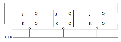
- a)

- b)

- c)

- d)

Correct answer is option 'C'. Can you explain this answer?
A 3 stage Johnson counter (ring) shown in figure is clocked at a constant frequency of fc from the starting state of Q0 Q1 Q2 = 101. The frequency of output Q0 Q1 Q2 will be
a)
b)
c)
d)
 | Hrithik Kallem answered |
Q0 Q1 Q2
1 0 1
0 1 0
1 0 1
0 1 0
Q0 repeats after every 2 cycles,freq of Q0 is f/2
Q1 repeats after every 2 cycles,freq of Q1 is f/2
Q2 repeats after every 2 cycles,freq of Q2 is f/2
so, total output freq is f/6.
1 0 1
0 1 0
1 0 1
0 1 0
Q0 repeats after every 2 cycles,freq of Q0 is f/2
Q1 repeats after every 2 cycles,freq of Q1 is f/2
Q2 repeats after every 2 cycles,freq of Q2 is f/2
so, total output freq is f/6.
Chapter doubts & questions for Practice Tests: Digital Electronics - Digital Electronics 2026 is part of Electrical Engineering (EE) exam preparation. The chapters have been prepared according to the Electrical Engineering (EE) exam syllabus. The Chapter doubts & questions, notes, tests & MCQs are made for Electrical Engineering (EE) 2026 Exam. Find important definitions, questions, notes, meanings, examples, exercises, MCQs and online tests here.
Chapter doubts & questions of Practice Tests: Digital Electronics - Digital Electronics in English & Hindi are available as part of Electrical Engineering (EE) exam. Download more important topics, notes, lectures and mock test series for Electrical Engineering (EE) Exam by signing up for free.
Digital Electronics113 videos|91 docs|58 tests |