Electronics and Communication Engineering (ECE) Exam  >  Electronics and Communication Engineering (ECE) Tests  >  ISRO Scientist ECE Mock Test Series 2025  >  ISRO Scientist Electronics Mock Test - 1 - Electronics and Communication Engineering (ECE) MCQ

ISRO Scientist Electronics Mock Test - 1 - Electronics and Communication Engineering (ECE) MCQ


Test Description

30 Questions MCQ Test ISRO Scientist ECE Mock Test Series 2025 - ISRO Scientist Electronics Mock Test - 1

ISRO Scientist Electronics Mock Test - 1 for Electronics and Communication Engineering (ECE) 2025 is part of ISRO Scientist ECE Mock Test Series 2025 preparation. The ISRO Scientist Electronics Mock Test - 1 questions and answers have been prepared according to the Electronics and Communication Engineering (ECE) exam syllabus.The ISRO Scientist Electronics Mock Test - 1 MCQs are made for Electronics and Communication Engineering (ECE) 2025 Exam. Find important definitions, questions, notes, meanings, examples, exercises, MCQs and online tests for ISRO Scientist Electronics Mock Test - 1 below.
Solutions of ISRO Scientist Electronics Mock Test - 1 questions in English are available as part of our ISRO Scientist ECE Mock Test Series 2025 for Electronics and Communication Engineering (ECE) & ISRO Scientist Electronics Mock Test - 1 solutions in Hindi for ISRO Scientist ECE Mock Test Series 2025 course. Download more important topics, notes, lectures and mock test series for Electronics and Communication Engineering (ECE) Exam by signing up for free. Attempt ISRO Scientist Electronics Mock Test - 1 | 95 questions in 120 minutes | Mock test for Electronics and Communication Engineering (ECE) preparation | Free important questions MCQ to study ISRO Scientist ECE Mock Test Series 2025 for Electronics and Communication Engineering (ECE) Exam | Download free PDF with solutions
ISRO Scientist Electronics Mock Test - 1 - Question 1

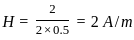
The magnetic field intensity at the centre of a circular coil of diameter 1 meter and carrying a current of 2 ampere is ______.

Detailed Solution for ISRO Scientist Electronics Mock Test - 1 - Question 1

Concept:
The magnetic field intensity (H) of a circular coil is given by
H  = I/2R
Where I is the current flow through the coil
R is the radius of the circular coil

Calculation:
Given that, Current (I) = 2 A
Diameter = 1 m
Radius (R) = 0.5 m

Magnetic field intensity

ISRO Scientist Electronics Mock Test - 1 - Question 2

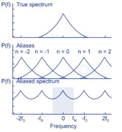
A single tone 4 kHz message signal is sampled with 10 kHz and 6 kHz. Aliasing effect will be seen in the reconstructed signal when the signal is sampled with

Detailed Solution for ISRO Scientist Electronics Mock Test - 1 - Question 2

Concept:
The sampling theorem states that “a signal can be exactly reproduced if it is sampled at the rate fs which is greater than twice the maximum frequency W in the modulating signal."

If the sampled frequency is less than the Nyquist frequency, overlapping of lower and upper sidebands known as aliasing takes place.

The main reason for aliasing is under-sampling, i.e. sampling the signal at a frequency less than twice the Nyquist rate.
fs < 2fm
fs = Sampling frequency
fm = Modulating frequency

Application:
The minimum sampling rate to avoid aliasing will be:
fs = 2 × 2fm = 2 × 4 kHz
fs = 8 kHz
∴ For 6 kHz, the Aliasing effect will be seen in the reconstructed signal as the sampling frequency is less than the Nyquist Rate.

Important Point

Aliasing is explained with the help of the spectrum as shown:

ISRO Scientist Electronics Mock Test - 1 - Question 3

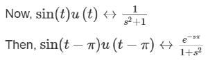
The Laplace Transform of the following signal is:

Detailed Solution for ISRO Scientist Electronics Mock Test - 1 - Question 3

Concept:
If f(t) ↔ F(s)
Then, f(t - t0) ↔ F(s).e-sto

Calculation:
The given signal can be represented as the multiplication of the below two functions:


i.e. the given signal can be presented as:
= (sin t) [u(t) - u(t - π]
= sin t u(t) - sin t u(t - π)
Now, sin (t - π) = -sin t
So, the above can be represented as;
= sin t u(t) + sin (t - π) u(t - π)

So, the Laplace transform of sin t u(t) + sin (t - π) u(t - π) i.e. of the given signal is:

ISRO Scientist Electronics Mock Test - 1 - Question 4

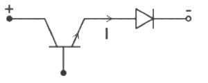
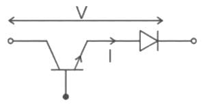
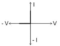
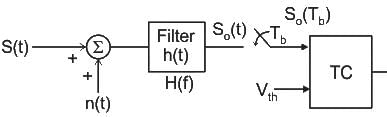
The following figure shows a composite switch consisting of a power transistor (BJT) in series with a diode. Assuming that the transistor switch and the diode are ideal, the I-V characteristic of the composite switch is

Detailed Solution for ISRO Scientist Electronics Mock Test - 1 - Question 4

Both the power transistor and the diode are ideal.
When voltage V is positive, both transistor and diode will be ON and making voltage across them zero and current I will be flowing.
⇒ at V = 0, I = Imaximum (∞)
When voltage V is negative, then both will be OFF and offering infinite resistance and hence voltage is maximum, and the current is zero.
⇒ at V = Vmax (∞), I = 0
Now, the V-I characteristics are as shown below.

ISRO Scientist Electronics Mock Test - 1 - Question 5

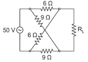
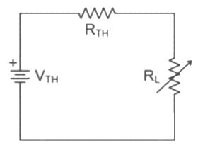
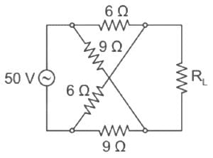
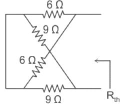
In the following network, the value of RL for the maximum power transfer and the maximum power is
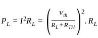
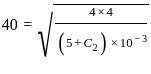
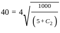
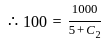
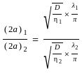
Detailed Solution for ISRO Scientist Electronics Mock Test - 1 - Question 5

Concept:

From the above circuit, the current flowing through the load, ‘I’ is given as

Power tranfered to the load,

In the above equation RL is a variable, therefore the condition for maximum power delivered to the load is determined by differentiating load power with respect to the load resistance and equating it to zero.

⇒ (RL + RTH)2 = 2RL (RTH + RL)
⇒ RL + RTH = 2RL
⇒ RL = RTH
This is the condition for maximum power transfer, which states that power delivered to the load is maximum, when the load resistance RL matches with Thevenin’s resistance RTH of the network.
Under this condition, power transfer to the load is
(by substituting RL = RTH)
Therefore, the power transfer to the load

Calculation:

By the above circuit diagram,
It obeys Wheatstone bridge i.e
6 × 9 = 6 × 9
The current across the load RL is zero
Vth = 0 V (by KVL)
That also implies the power across load RL is zero
Therefore, no power transfer across the load resistance RL
Note:

Rth = (6 6) + (9 9)
= 3 + 4.5
= 7.5 Ω

ISRO Scientist Electronics Mock Test - 1 - Question 6

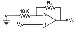
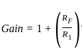
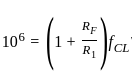
The op-amp shown in the figure has gain bandwidth product of 1 MHZ. If the closed loop bandwidth of the circuit is 100 KHZ, then value of feedback resistor RF is:

Detailed Solution for ISRO Scientist Electronics Mock Test - 1 - Question 6

Concept:
The gain bandwidth product of an op-amp is constant for both open loop as well as closed loop configuration.
AOL × FOL = ACL × fCL

Application:
For non-inverting amplifier


fCL = 100 KHZ = 105


RF = 9R1
RF = 90 KΩ

ISRO Scientist Electronics Mock Test - 1 - Question 7

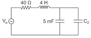
The circuit shown below is critically damped. The value of C2 is

Detailed Solution for ISRO Scientist Electronics Mock Test - 1 - Question 7

Concept:

In a series RLC circuit, the conditions for different nature of damping are:

Over damped:

Under damped:

Critically damped:

Calculation:
For critically damped system:

i.e,


5 + C2 = 10
C2 = 5 mF

ISRO Scientist Electronics Mock Test - 1 - Question 8

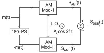
A balanced modulator is used in the generation of

Detailed Solution for ISRO Scientist Electronics Mock Test - 1 - Question 8

Balanced modulators and ring modulators are popularly used to generate DSB-SC signals.
The circuit diagram of a balanced modulator is as shown:


Balanced Modulator:-
1) It is used to generate a DSB-SC wave.
2) It consists of two AM modulators in a balanced configuration to suppress the carrier signal.
3) The message signal m(t) is applied at one modulator and – m(t) is applied at another modulator.

ISRO Scientist Electronics Mock Test - 1 - Question 9

An amplifier has voltage gain and current gain of 10 and 100 respectively. The voltage, current and power gain in decibels, respectively, will be:

Detailed Solution for ISRO Scientist Electronics Mock Test - 1 - Question 9

Concept:

  • A decibel is a one-tenth unit of the Bel (B) which is used to describe a gain of either voltage, current, or power.
  • It is used to describe the ratio of one magnitude of a power or field quantity to another, on a logarithmic scale, the logarithmic quantity being called a degree of power or a degree of field, respectively.

Let the voltage gain, current gain and power gain be X.
Voltage Gain (dB) = 20log(X)
Current Gain (dB) = 20log(X)
Power Gain (dB) = 10log(X)
log(10) = 1
log(Xn) = nlog(X)

Calculation:
Given:
Voltage Gain = 10
Current Gain = 100
Voltage Gain (dB) = 20log(10) = 20 dB
Current Gain (dB) = 20log(100) = 40log(10) = 40 dB

Power Gain (dB) = 10log(V × I)
Power Gain (dB) = 10log(10 × 100)
Power Gain (dB) = 10log(103) = 30 dB

ISRO Scientist Electronics Mock Test - 1 - Question 10
A Frequency Hopping Spread Spectrum system has its frequency synthesizers controlled by five stage shift-registers with feedback connections taken from the second and fifth stages. The number of slots available for frequency hopping is:
Detailed Solution for ISRO Scientist Electronics Mock Test - 1 - Question 10

Concept:

Frequency Hopping Spread Spectrum (FH-SS):

  • In FH-SS, the spectrum of the transmitted signal is spread sequentially by randomly hopping the data modulated carrier from one frequency to the next.
  • The synthesizer output at a given instant of time is the frequency hop.
  • The output bits of the PN generator change randomly. Hence the synthesizer output frequency will also change randomly.
  • If the number of successive bits at the output of the PN generator is n, then the total number of frequency hops will be 2n.

Calculation:

The number of register stages given is 5, i.e.

n = 5

∴ The number of slots available for frequency hopping will be:

Number of Slots = 2n = 25

= 32

ISRO Scientist Electronics Mock Test - 1 - Question 11

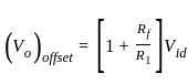
An op-amp based inverting amplifier with a gain of 100 and feedback resistance of 47 kΩ, the op-amp input offset voltage is 6 mV and input bias current is 500 nA. The output offset voltage due to an input offset voltage and an input bias current, are

Detailed Solution for ISRO Scientist Electronics Mock Test - 1 - Question 11

Concept:

Input offset voltage:

  • Whenever both the input terminals of the op-amp are grounded, ideally the output voltage must be zero. However, in this condition, the practical op-amp always shows a small non-zero output voltage.
  • The input offset voltage depends upon the temperature and given as:

Vid = V1 – V2

Input Bias current:

  • For ideal op-amp, no current flows into the input terminals but in a practical case, op-amp does have some very small input currents of the order 10-16 A to 10-14 A.
  • Therefore input bias current is defined as the current flowing into each of the two input terminals when they are biased to the same voltage level i.e. when the op-amp is balanced.

  • Output offset voltage (Vo)offset due to input offset is given by:

  • Output offset voltage (Vo)offset due to input bias current is given by:

(Vo)offset = RfIB
Rf = Feedback resistor
R1 = Input resistance of the Op-Amp

Calculation:
Given:

Gain = 100, Vid = 6 mV, Ib = 500 nA
Output offset voltage (Vo)offset due to input offset is:

(VO)Offset = (1 + 100) 6mV
(VO)Offset = 606 mV
Output offset voltage (Vo)offset due to input bias current is:
(Vo)offset = RfIB
(VO)Offset = 47 kΩ × 500 nA
(VO)Offset = 23.5 mV

ISRO Scientist Electronics Mock Test - 1 - Question 12

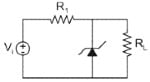
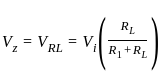
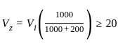
In the circuit shown, the breakdown voltage and the maximum current of the Zener diode are 20 V and 60 mA, respectively. The values of R1 and RL are 200 Ω and 1 kΩ, respectively. What is the range of Vi that will maintain the Zener diode in the ‘on’ state?

Detailed Solution for ISRO Scientist Electronics Mock Test - 1 - Question 12

For the zenor diode to be on minimum voltage across it should be 20V.

Vi ≥ 20 x 1200/1000
Vi ≥ 24 V
Only option (B) satisfies this condition.
This objective approach solves time to calculate the upper bound on Vi

ISRO Scientist Electronics Mock Test - 1 - Question 13

A good transimpedance amplifier has

Detailed Solution for ISRO Scientist Electronics Mock Test - 1 - Question 13

Transresistance or trans-impedance amplifier is normally used as a current to voltage converter which requires low input and low output impedances for its proper operation.
Requirements of input and output impedances for different amplifiers are listed below:

ISRO Scientist Electronics Mock Test - 1 - Question 14

A parallel plate capacitor of 100 pf having an air dielectric is charged to 10 kilovolts. It is then electrically isolated. The plates are pulled away from each other until the distance is ten times more than before. Estimate the energy needed to pull the plates.

Detailed Solution for ISRO Scientist Electronics Mock Test - 1 - Question 14

The distance between the plates of the capacitor is increased 10 times since:
C = εA/d
The capacitance decreases 10 times:
Cnew = C/10
The plates of the capacitor are isolated electrically ⇒ q, the charge is constant
q = CV
⇒ Voltage becomes 10 times previous value Vnew = 10 kV
Energy initially stored in capacitance is E = 1/2 CV2 = 1/2 x 100 x 10-12 x (104)2 
= 0.005 J
Energy after plates are moved to 10 times the original distance:
Enew = 1/2 Cnew ​​​​​​​ V2new
= 1/2 C/10 (10V)2
= 10 X 1/2CV2

= 0.05 J

ISRO Scientist Electronics Mock Test - 1 - Question 15

A communication channel with Addictive White Gaussian Noise, has a bandwidth of 4 kHz and SNR of 31 dB. Its channel capacity is

Detailed Solution for ISRO Scientist Electronics Mock Test - 1 - Question 15

Concept:
The capacity of a band-limited AWGN channel is given by the formula:
C = Blog2( 1 + (S/N)
C = Maximum achievable data rate (in bits/sec)
B = channel bandwidth
S/N = signal Noise power (in W)
Note: In the expression of channel capacity, S/N is expressed not in dB.
Calculation:
Given B.W. = 4 kHz, S/N = 31 dB
Since the S/N ratio is in dB, we can write:
10log10(S/N) = 31
10log10(S/N) = 3.1
S/N = 103.1W
The channel capacity will be:
C = (4 x 10³) log2 ( 1 + 103.1)
C = 41.19 kbps
The closest option is 32 kbps. Mistake Points Many of us will make a common mistake of selecting 20 kbps as the correct answer, which can't be right. Because, in the formula of channel capacity S/N is not in dB, it is in Watts.

ISRO Scientist Electronics Mock Test - 1 - Question 16

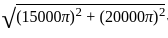
An angle modulated signal with carrier frequency ωc = 2π × 105 rad/sec is described by the equation

s(t) = 10 cos (ωct + 5 sin (3000 πt) + 10 sin (2000 πt)).

What is the frequency deviation Δf?

Detailed Solution for ISRO Scientist Electronics Mock Test - 1 - Question 16

​The maximum frequency deviation is:

= 12500 Hz

ISRO Scientist Electronics Mock Test - 1 - Question 17

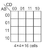
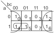
What will be the simplified Boolean function of the given equation?

F(a, b, c) = ∑(0, 2, 4, 5, 6)

Detailed Solution for ISRO Scientist Electronics Mock Test - 1 - Question 17

Concept:
The K-map is a graphical method that provides a systematic method for simplifying and manipulating the Boolean expressions or to convert a truth table to its corresponding logic circuit in a simple, orderly process.
In an 'n' variable K map, there are 2n cells
For 4 variables there will be 24 = 16 cells as shown:

Calculations:
F(a, b, c) = ∑(0, 2, 4, 5, 6)

F = c' + ab'

ISRO Scientist Electronics Mock Test - 1 - Question 18

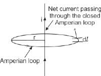
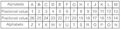
According to Ampere's circuital Law, The Line Integral of H about any closed path is exactly _______ to the direct current enclosed by that path.

Detailed Solution for ISRO Scientist Electronics Mock Test - 1 - Question 18

Concept:
Ampere's Circuital Law:

  • It gives the relationship between the current and the magnetic field created by it.
  • This law says that the integral of magnetic field density (B) along an imaginary closed path is equal to the product of current enclosed by the path and permeability of the medium.

Where dl is a small element, μ0 is the permeability of free space and I is the electric current.

ISRO Scientist Electronics Mock Test - 1 - Question 19
The polar plot of a transfer function with ω as the parameter is known as the
Detailed Solution for ISRO Scientist Electronics Mock Test - 1 - Question 19

Nyquist plot:

Nyquist plots are an extension of polar plots for finding the stability of the closed-loop control systems. This is done by varying ω from −∞ to ∞, i.e. Nyquist plots are used to draw the complete frequency response of the open-loop transfer function.

Method of drawing Nyquist plot:

  • Locate the poles and zeros of open-loop transfer function G(s)H(s) in ‘s’ plane.
  • Draw the polar plot by varying ω from zero to infinity.
  • Draw the mirror image of the above polar plot for values of ω ranging from −∞ to zero.
  • The number of infinite radii half circles will be equal to the number of poles at the origin.
  • The infinite radius half-circle will start at the point where the mirror image of the polar plot ends. And this infinite radius half-circle will end at the point where the polar plot starts.
ISRO Scientist Electronics Mock Test - 1 - Question 20

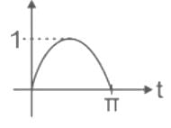
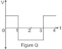
The voltage waveform in figure Q is applied across an ideal inductor. What is the resulting current waveform?

Detailed Solution for ISRO Scientist Electronics Mock Test - 1 - Question 20

CONCEPT:
Inductors: The coils of wire that are wound around any ferromagnetic material (iron cored) or wound around a hollow tube that increase their inductive value are called inductors.

  • The inductance (L) is measured in Henry (H) and the instantaneous voltage in volts.
  • Rate of instantaneous voltage is given by (v = L di/dt)

Analysis:
By integrating the voltage we will get the current,
the voltage is a rectangular function hence the current will be a ramp function.
Hence, option 1 is correct.

ISRO Scientist Electronics Mock Test - 1 - Question 21
For a second order system the undamped natural frequency is 3 rad/sec. and the damped frequency is 2.4 rad/sec. The damping ratio is
Detailed Solution for ISRO Scientist Electronics Mock Test - 1 - Question 21

Concept:

Damped natural frequency of a second order system is given by

Where,

ωn = Natural frequency

ζ = Damping ratio

Calculation:

Given-

ωn = 3 rad/sec

Now, natural damped frequency can be calculated as

ζ2 = 1 - (2.4/3)2

ζ = 0.6

ISRO Scientist Electronics Mock Test - 1 - Question 22

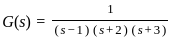
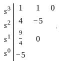
A unity feedback system has the open loop transfer function 
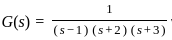
. How many times the Nyquist plot of G(s) encircles the (-1, 0) point ?

Detailed Solution for ISRO Scientist Electronics Mock Test - 1 - Question 22


For Nyquist plot of G(s), encirclements is
N = P – Z
Where P = right side poles of open loop transfer function
The characteristic equation is:
1 + (s-1)(s+2)(s+3) = 0
(s2 + 5s + 6)(s - 1) + 1 = 0
s3 + 5s2 + 6s - s2 - 5s - 6 + 1 = 0
s3 + 4s2 + s - 5 = 0

Z = right half-plane pole
Z = 1, P = 1.
⇒ N = 1 – 1 = 0
Therefore, the Nyquist plot never encircles (-1 + j0)

ISRO Scientist Electronics Mock Test - 1 - Question 23
Two parabolic reflector antennas operated at 100 MHz and 200 MHz respectively have the same directivity. Assuming that the aperture efficiency of the antenna is 40% and 80% respectively, then the ratio of the diameter of antenna 1 to antenna 2 is (approximately) _______.
Detailed Solution for ISRO Scientist Electronics Mock Test - 1 - Question 23

Concept :

The directivity for an antenna is mathematically calculated as:

η = Efficiency

a = Radius

Rearranging the above, we get:

Calculation:

Given:

f1 = 100 MHz, f2 = 200 MHz, η1 = 40%, η2 =80%

The ratio of the diameter of antenna 1 to antenna 2 will be:

Since √2 = 1.41, we the required ratio will be:

= 1.41 × 2 = 2.82

ISRO Scientist Electronics Mock Test - 1 - Question 24


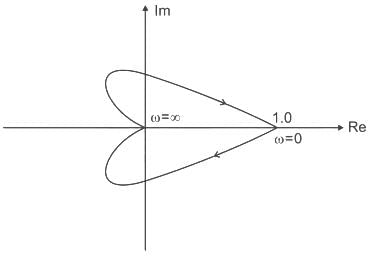
The Nyquist plot shown above, matches with the transfer function

Detailed Solution for ISRO Scientist Electronics Mock Test - 1 - Question 24

From the given Nyquist plot
At ω = 0, 1 ∠0°
ω = ∞, 0∠-180°
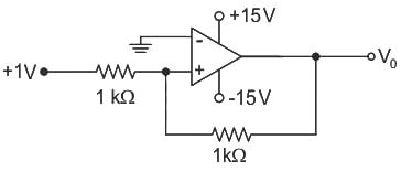
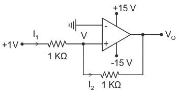
matches these conditions.

ISRO Scientist Electronics Mock Test - 1 - Question 25
For an n-channel MOSFET, if conduction parameter (kn) is 0.249 mA/V2, gate to source voltage VQS is 2VTN where VTN = 0.75V. The current will be
Detailed Solution for ISRO Scientist Electronics Mock Test - 1 - Question 25

Concept:

For an n-channel MOSFET, the current in triode and saturation region is given by:

ID = Kn [2VDS(VGS - Vth) - VDS2)] when VDS < VGS - Vth

when VDS > VGS - Vth

VDS = Drain to Source Voltage

VGS = Gate to source voltage

Vth = Threshold Voltage

Kn = Conduction parameter

Analysis:

Given: Kn = 0.249 mA / V2

VGS = 2VTN

VTN = 0.75 V

∵ VGS – VTN = 0.75 V

And VDS is usually more than that

∴ VDS > VGS - VTN

And the MOSFET is in saturation.

ID = 0.249 (2VTN - VTN)2

= 0.249 (VTN)2

= 0.249 (0.75)2

= 0.14 mA

ISRO Scientist Electronics Mock Test - 1 - Question 26

In the circuit of the ideal Op-Amp, V0 is

Detailed Solution for ISRO Scientist Electronics Mock Test - 1 - Question 26

By redrawing the circuit, we get

As shown in the circuit diagram, given op-amp is inverted grounded and output is corresponding to the non-inverted terminal.
∴ V = +Vcc = 15 volt
Now by applying KCL at node ‘V’ we get
I1 = I2

1 – V = V – V0
V0 = 2V - 1
V0 = 29 volt
But output voltage can't be greater than higher saturation voltage (Vcc)
∴ Output voltage (V0) = +15 volt

ISRO Scientist Electronics Mock Test - 1 - Question 27

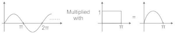
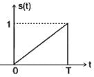
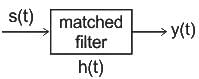
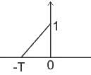
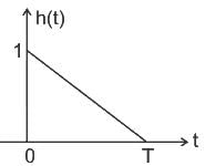
Consider the pulse shape s(t) as shown. The impulse response h(t) of the filter matched to this pulse is

Detailed Solution for ISRO Scientist Electronics Mock Test - 1 - Question 27

Concept:
The shown bock diagram will be considered as the receiver in digital communication.

The impulse response of the filter is calculated by:

h(t) = s*(Tb - t)
Calculation:
In the given signal the duration is T. So, Tb = T
The shifted signal by T is given by:
s(t+T)

The time-reversed signal will be

Option 3 is correct.

ISRO Scientist Electronics Mock Test - 1 - Question 28

The given bar graph shows the data of production of pulses (in lakh tonnes) by three different countries X, Y and Z over the years. Study the bar graph and answer tha question that follows.

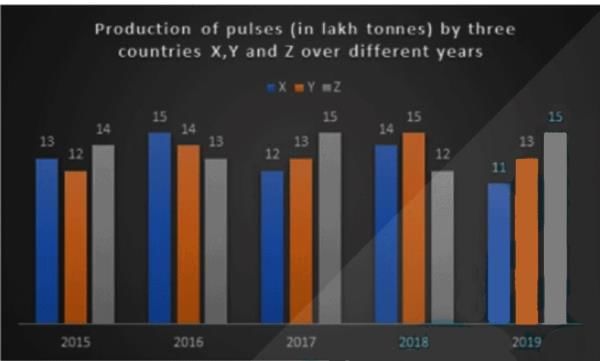
For which country is the average production (in lakh tonnes) for five years the maximum?

Detailed Solution for ISRO Scientist Electronics Mock Test - 1 - Question 28

Calculation:
Total production of X in 5 years = 13 + 15 + 12 + 14 + 11
⇒ 65
Average = 65/5
⇒ 13
Total production of Y in 5 years = 12 + 14 + 13 + 15 + 13
⇒ 67
Average = 67/5
⇒ 13.4
Total production of Z in 5 years = 14 + 13 + 15 + 12 + 15
⇒ 69
Average = 69/5
⇒ 13.8
∴ The requied answer is Z.

ISRO Scientist Electronics Mock Test - 1 - Question 29

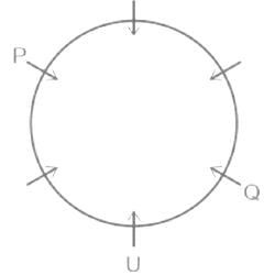
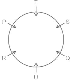
P, Q, R, S, T and U are sitting around a circular table, facing the centre. P sits second to the left of U and third to the right of Q. S sits second to the right of U. R sits second to the left of Q. Who is immediate neighbour of Q and T both?

Detailed Solution for ISRO Scientist Electronics Mock Test - 1 - Question 29

Persons: P, Q, R, S, T and U

With the help of the information given in the question, we can draw the arrangement,

Step 1: P sits second to the left of U and third to the right of Q.

Step 2: S sits second to the right of U.

Step 3: R sits second to the left of Q. Therefore the remaining spot is assigned to T.

From the diagram, we can see that the immediate neighbor of both Q and T is S.

Hence the correct answer is S.

ISRO Scientist Electronics Mock Test - 1 - Question 30

Select the option that is related to the third letter-cluster in the same way as the second letter-cluster is related to the first letter-cluster.

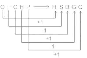
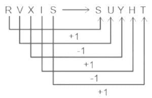
GTCHP : HSDGQ :: RVXIS : ?

Detailed Solution for ISRO Scientist Electronics Mock Test - 1 - Question 30

The logic followed here is :-

  • GTCHP : HSDGQ

Similarly,

  • RVXIS : ?

Hence, the correct answer is "SUYHT".

View more questions
3 tests
Information about ISRO Scientist Electronics Mock Test - 1 Page
In this test you can find the Exam questions for ISRO Scientist Electronics Mock Test - 1 solved & explained in the simplest way possible. Besides giving Questions and answers for ISRO Scientist Electronics Mock Test - 1, EduRev gives you an ample number of Online tests for practice
Download as PDF