Semiconductor Diode MCQ Level – 1 - Physics MCQ
10 Questions MCQ Test - Semiconductor Diode MCQ Level – 1
The correct sequence of band gaps of germanium  silicon
 and gallium arsenide
 will :
 silicon
 and gallium arsenide
 will :
Identify the condition for a transistor to act as an amplifier.
A zener diode is also a p-n junction diode. It can be used as :
The electrical conductivity of a semiconductor increases when electromagnetic radiation of a wavelength shorter than 2480 nm is incident on it. The band gap (in eV) for the semiconductor is?
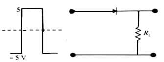
If in a p-n junction diode, a square input signal of 8V is applied (see figure below), what is the value of output signal across RL?

The impurity atoms with which pure silicon should be doped to make p-type semiconductor are those of .
What is the maximum electric field when Vbi = 2V, VR = 5V and width of the semiconductor is 7cm?
The fermi level of an intrinsic semi-conductor is pinned at the centre of the band-gap. The probability of occupation of the highest electronic state in valence band at room temperature, will b e :
The depletion layers in a p-n junction diode consists of layers of :
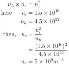
pure silicon at 300K has equal electrons concentrations (ne) and hole concentration (nh) of 1.5 x 10¹⁶ m-3 . Doping by sodium increases nh to 4.5 x 10²² m-3 . Then ne in the doped silicon is :


 where ni is the concentration of intrinsic semiconductor


