Electrical Engineering (EE) Exam  >  Electrical Engineering (EE) Tests  >  Electrical Engineering SSC JE (Technical)  >  Test: Basic Electronics - 1 - Electrical Engineering (EE) MCQ

Test: Basic Electronics - 1 - Electrical Engineering (EE) MCQ


Test Description

25 Questions MCQ Test Electrical Engineering SSC JE (Technical) - Test: Basic Electronics - 1

Test: Basic Electronics - 1 for Electrical Engineering (EE) 2024 is part of Electrical Engineering SSC JE (Technical) preparation. The Test: Basic Electronics - 1 questions and answers have been prepared according to the Electrical Engineering (EE) exam syllabus.The Test: Basic Electronics - 1 MCQs are made for Electrical Engineering (EE) 2024 Exam. Find important definitions, questions, notes, meanings, examples, exercises, MCQs and online tests for Test: Basic Electronics - 1 below.
Solutions of Test: Basic Electronics - 1 questions in English are available as part of our Electrical Engineering SSC JE (Technical) for Electrical Engineering (EE) & Test: Basic Electronics - 1 solutions in Hindi for Electrical Engineering SSC JE (Technical) course. Download more important topics, notes, lectures and mock test series for Electrical Engineering (EE) Exam by signing up for free. Attempt Test: Basic Electronics - 1 | 25 questions in 50 minutes | Mock test for Electrical Engineering (EE) preparation | Free important questions MCQ to study Electrical Engineering SSC JE (Technical) for Electrical Engineering (EE) Exam | Download free PDF with solutions
Test: Basic Electronics - 1 - Question 1

The emitter of a transistor is doped the heaviest because of it :

Detailed Solution for Test: Basic Electronics - 1 - Question 1

The reason the emitter is the most heavily doped region is because it serves to inject a large amount of charge carriers into the base, which then travels into the collector, so that switching or amplification can occur.

Test: Basic Electronics - 1 - Question 2

Voltage power supplies use a high resistance across the output of the supply. That resistance is called

Detailed Solution for Test: Basic Electronics - 1 - Question 2

Bleeder resistors are standard high value resistors which are used to discharge the capacitor in filter circuit. The discharging of the capacitors is really important because even if the power supply is OFF, a charged capacitor can give a shock to anybody.

1 Crore+ students have signed up on EduRev. Have you? Download the App
Test: Basic Electronics - 1 - Question 3

For a NPN bipolar transistor, what is the main stream of current in the base region?​

Detailed Solution for Test: Basic Electronics - 1 - Question 3

Diffusion current is a current in a semiconductor caused by the diffusion of charge carriers (holes and/or electrons). Diffusion current can be in the same or opposite direction of a drift current.

Test: Basic Electronics - 1 - Question 4

The current ICBO flows in the

Detailed Solution for Test: Basic Electronics - 1 - Question 4

ICBO is the collector current with collector junction reverse biased and base open-circuited. ICEO is the collector current with collector junction reverse biased and emitter open-circuited.  ICBO is reverse leakage current going from the Collector to the Base. 

Test: Basic Electronics - 1 - Question 5

Two P-N junction diodes are connected back to back to make a transistor. Which one of the following is correct?

Detailed Solution for Test: Basic Electronics - 1 - Question 5

This doesn't work because base region is wide and are equally doped, whereas in actual transistor base is very thin and lightly doped. In two discrete diodes connected back-to-back, has 4 doped regions instead of 3. Hence, two diodes connected back-to-back can never be used as a transistor.

Test: Basic Electronics - 1 - Question 6

The alpha (a) and beta (b) of a transistor are related to each other as

Detailed Solution for Test: Basic Electronics - 1 - Question 6

The relationship between alpha (a) and beta (b) of a transistor is given by the equation:
a = b / (1 + b)
To understand this relationship, let's break it down step by step:
1. Alpha (a): Alpha is the ratio of collector current (Ic) to emitter current (Ie) in a transistor. It represents the fraction of current flowing from the collector to the emitter.
2. Beta (b): Beta is the ratio of collector current (Ic) to base current (Ib) in a transistor. It represents the amplification factor of a transistor.
3. Relationship: The equation a = b / (1 + b) shows that alpha is directly proportional to beta. As the value of beta increases, the value of alpha also increases.
4. Interpretation: The equation indicates that alpha is always less than beta. In other words, the current flowing from the collector to the emitter is always less than the current flowing from the collector to the base.
5. Example: Let's assume the value of beta is 100. Substituting this value in the equation, we get:
a = 100 / (1 + 100) = 100 / 101 = 0.99
This means that for a beta value of 100, the alpha value is approximately 0.99.
In conclusion, the relationship between alpha and beta in a transistor is given by the equation a = b / (1 + b), where alpha is directly proportional to beta.
Test: Basic Electronics - 1 - Question 7

ICBO in transistor can be reduced by reducing

Detailed Solution for Test: Basic Electronics - 1 - Question 7

To reduce the collector current (ICBO) in a transistor, the following steps can be taken:
1. Reduce the Base Current (IB):
- The collector current (IC) is directly proportional to the base current (IB) according to the transistor's current gain (hfe).
- By reducing the base current, the collector current can be reduced, which in turn reduces the collector-base leakage current (ICBO).
2. Reduce the Supply Voltage (VCC):
- The collector-base leakage current (ICBO) is also dependent on the supply voltage (VCC).
- By reducing the supply voltage, the collector-base leakage current can be reduced.
3. Reduce the Emitter Current (IE):
- The collector current (IC) is also directly proportional to the emitter current (IE).
- By reducing the emitter current, the collector current and collector-base leakage current can be reduced.
4. Reduce the Temperature:
- The collector-base leakage current (ICBO) increases with temperature.
- By reducing the temperature, the collector-base leakage current can be reduced.
Therefore, the correct answer is option D: temperature. By reducing the temperature, the collector-base leakage current (ICBO) in a transistor can be reduced.
Test: Basic Electronics - 1 - Question 8

Ebers-Model of transistor represents two diodes

Detailed Solution for Test: Basic Electronics - 1 - Question 8
Ebers-Model of Transistor and Representation of Diodes
The Ebers-Model of a transistor is a mathematical model that describes the behavior and characteristics of a bipolar junction transistor (BJT). It is commonly used to analyze and design transistor circuits. In the Ebers-Model, the transistor is represented by two diodes, which are connected in a specific way to reflect the behavior of the BJT.
The answer to the given question is option C: Back to back.
Explanation of the representation of diodes in the Ebers-Model:
1. The Ebers-Model considers the two types of charge carriers in a BJT, namely electrons and holes, and models their behavior in different regions of the transistor.
2. The base-emitter junction is represented by a forward-biased diode. This diode consists of a p-n junction with the p-type material connected to the base terminal and the n-type material connected to the emitter terminal.
3. The base-collector junction is represented by a reverse-biased diode. This diode consists of a p-n junction with the p-type material connected to the base terminal and the n-type material connected to the collector terminal.
4. The diodes are connected back to back, which means their anodes and cathodes are connected together. This configuration reflects the physical arrangement of the base-emitter and base-collector junctions in a BJT.
5. The Ebers-Model uses the diode representations to describe the current-voltage characteristics of the BJT. It considers the forward and reverse biasing of the diodes to analyze the transistor's behavior in different operating regions.
In conclusion, the Ebers-Model of a transistor represents two diodes connected back to back. This representation helps in analyzing the behavior and characteristics of the transistor in different operating conditions.
Test: Basic Electronics - 1 - Question 9

Application of DC voltage to a diode, transistor, or other device to produce a desired mode of operation is called

Detailed Solution for Test: Basic Electronics - 1 - Question 9
Biasing:
- Biasing is the process of applying a DC voltage to a diode, transistor, or other electronic device in order to establish the desired operating conditions.
- It ensures that the device operates in the desired mode and produces the desired output.
- Biasing is crucial in electronic circuit design as it determines the operating point, stability, and linearity of the device.
Importance of Biasing:
- Proper biasing is essential for the device to function correctly and reliably.
- It ensures that the device operates within its specified voltage and current ranges.
- Biasing also helps in achieving desired amplification, switching, or rectification characteristics.
Types of Biasing:
1. Fixed Bias: A fixed DC voltage is applied to the device using resistors and a power supply. It provides a stable operating point but is sensitive to variations in temperature and device characteristics.
2. Self-Bias: The biasing voltage is generated internally by the device itself, eliminating the need for external biasing components. It offers improved stability but may be less precise.
3. Emitter Bias: Biasing is achieved by connecting a resistor between the emitter and ground. It provides stability and compensates for variations in temperature.
4. Collector Bias: Biasing is done by connecting a resistor between the collector and the power supply. It offers stability but may be affected by changes in the power supply voltage.
Effects of Biasing:
- Under-biasing: Insufficient bias voltage can lead to distortion, non-linearity, and poor device performance.
- Over-biasing: Excessive bias voltage can cause power dissipation, reduced efficiency, and potential device failure.
- Proper biasing ensures optimal performance, efficiency, and reliability of the device.
In conclusion, biasing is the application of a DC voltage to establish desired operating conditions for electronic devices. It is important for achieving the desired mode of operation and ensuring proper performance and reliability. Different types of biasing methods can be used depending on the specific requirements of the device and the desired output.
Test: Basic Electronics - 1 - Question 10

The phenomenon known as "Early Effect" in a bipolar transistor refers to a reduction of the effective base-width caused by

Detailed Solution for Test: Basic Electronics - 1 - Question 10
The Early Effect in a Bipolar Transistor

The phenomenon known as the "Early Effect" in a bipolar transistor refers to a reduction of the effective base-width caused by:


Explanation:
Bipolar Transistor Basics:
- A bipolar transistor consists of three layers: the emitter, base, and collector.
- The base region is typically lightly doped compared to the emitter and collector regions.
Early Effect:
- The Early Effect, also known as the base-width modulation effect, refers to a decrease in the effective base width as the collector-base voltage increases.
- This effect reduces the base current and affects the transistor's performance.
Causes of the Early Effect:
- The reduction of the effective base width is primarily caused by the reverse biasing of the base-collector junction.
- As the collector-base voltage increases, the depletion region widens, shrinking the base width.
- This narrowing of the base width results in a decrease in the transit time of charge carriers through the base region.
Effect on Transistor Performance:
- The Early Effect can lead to a decrease in the current gain of the transistor, which affects its amplification capabilities.
- It also affects the frequency response and can introduce distortion in the output signal.
- Designers must consider the Early Effect when designing transistor circuits to ensure proper performance.
Therefore, the correct answer is B: the reverse biasing of the base-collector junction.
Test: Basic Electronics - 1 - Question 11

Which one of the following specifications is not correct for a common collector amplifier ?

Detailed Solution for Test: Basic Electronics - 1 - Question 11
Common Collector Amplifier Specifications
The common collector amplifier, also known as the emitter follower, is a type of transistor amplifier configuration. It has the following specifications:
1. High input impedance:
- This means that the input impedance of the common collector amplifier is high, which allows it to interface with high impedance sources without loading them.
- In other words, it does not draw much current from the input source, ensuring minimal signal attenuation.
2. Low output impedance:
- The common collector amplifier has a low output impedance, which means it can drive low impedance loads without significant signal loss.
- This characteristic enables it to provide a strong and stable output signal.
3. High voltage gain:
- The common collector amplifier exhibits a high voltage gain, which is the ratio of the change in output voltage to the change in input voltage.
- It amplifies the input signal voltage, making it useful for applications where voltage amplification is required.
4. High current gain:
- The common collector amplifier also has a high current gain, which is the ratio of the change in output current to the change in input current.
- It can provide a high output current while drawing a relatively small input current.
Answer:
The specification that is not correct for a common collector amplifier is High voltage gain (Option C).
- The common collector amplifier has a unity voltage gain or a voltage gain slightly less than unity.
- It acts as a voltage buffer, providing a low output impedance and high input impedance, but it does not amplify the input voltage significantly.
Therefore, the correct answer is option C: High voltage gain.
Test: Basic Electronics - 1 - Question 12

In a common collector amplifier the voltage gain is

Detailed Solution for Test: Basic Electronics - 1 - Question 12

The output voltage on a common-collector amplifier will be in phase with the input voltage, making the common-collector a non-inverting amplifier circuit. The current gain of a common-collector amplifier is equal to β plus 1. The voltage gain is approximately equal to 1 (in practice, just a little bit less).

Test: Basic Electronics - 1 - Question 13

The transistor configuration which provides highest output impedance is :

Detailed Solution for Test: Basic Electronics - 1 - Question 13


In Common-Base Transistor, the base-emitter junction JE at input side acts as a forward biased diode. So, the common base amplifier has a low input impedance (low opposition to incoming current). On the other hand, the collector-base junction JC at output side acts somewhat like a reverse biased diode. So the common base amplifier has high output impedance.

Therefore, the common base amplifier provides a low input impedance and high output impedance.

Test: Basic Electronics - 1 - Question 14

In cutoff region in an N-P-N transistor

Detailed Solution for Test: Basic Electronics - 1 - Question 14

Whenever we observe the terminals of a BJT and see that the emitter-base junction is not at least 0.6-0.7 volts, the transistor is in the cutoff region. In cutoff, the transistor appears as an open circuit between the collector and emitter terminals. As is seen in 2, this implies Vout is equal to 10 volts.
In cutoff region in an N-P-N transistor VCB is + Ve and VBE is – ve
These are the transistor characteristics.

Test: Basic Electronics - 1 - Question 15

Consider the following statements in respect of a CC amplifier.
1. It performs a resistance transformation from low to high resistance.
2. Its current gain is close to unity
3. Its voltage gain is close to unity
4. Its frequency range is higher than that of a CE-stage.
Which of the statements is given above are correct?

Detailed Solution for Test: Basic Electronics - 1 - Question 15

The correct statements regarding a CC amplifier are as follows:
1. It performs a resistance transformation from low to high resistance: A CC (Common Collector) amplifier, also known as an emitter follower, has a high input resistance and a low output resistance. It provides a resistance transformation from a low load resistance to a high input resistance. This allows it to match impedance between different stages of a circuit.
2. Its current gain is close to unity: The current gain of a CC amplifier is close to unity. It means that the output current is almost equal to the input current. The input current is amplified by a small factor, typically slightly less than 1.
3. Its voltage gain is close to unity: This statement is incorrect. The voltage gain of a CC amplifier is less than unity. It is slightly less than 1 due to the voltage drop across the emitter resistor. The CC amplifier is mainly used for impedance matching rather than voltage amplification.
4. Its frequency range is higher than that of a CE-stage: This statement is correct. The CC amplifier has a higher frequency range compared to a CE (Common Emitter) stage. It has a higher bandwidth and better high-frequency response due to its low input capacitance and low output capacitance.
Therefore, the correct statements are 1, 2, and 4. So, the answer is option A: 1, 2, and 4.
Test: Basic Electronics - 1 - Question 16

when a transistor is used in switching mode then what is the turn on time ?

Detailed Solution for Test: Basic Electronics - 1 - Question 16

Turn-on time of the transistor is the time taken by the transistor from the instant the pulse is applied to the instant the transistor switches into the ON state and is the sum of the delay time (td) and rise time (tr).

T(on) tr td
To find out the turn-on time of the transistor, the delay time and rise time have to be calculated.

Test: Basic Electronics - 1 - Question 17

For transistor, turn-off time is:

Detailed Solution for Test: Basic Electronics - 1 - Question 17

Turn-off time (TOFF) − The sum of storage time (ts) and fall time (tf) is defined as the Turn-off time.

Test: Basic Electronics - 1 - Question 18

The voltage divider bias circuit is used in amplifiers quite often becuase it

Detailed Solution for Test: Basic Electronics - 1 - Question 18
The Voltage Divider Bias Circuit
The voltage divider bias circuit is commonly used in amplifiers for various reasons. Let's explore the specific benefits of this circuit and why it is frequently employed:
Makes the operating point almost independent ofb
- The voltage divider bias circuit helps stabilize the operating point of the amplifier, making it less susceptible to variations in the transistor's characteristics.
- By providing a stable bias voltage, the circuit ensures that the transistor operates within its desired range. This helps maintain the amplifier's performance and prevents distortion.
Reduces the DC base current
- The voltage divider bias circuit minimizes the DC base current flowing through the transistor.
- This reduction in current helps improve the overall efficiency of the amplifier and reduces power consumption.
- It also helps prevent excessive heating of the transistor due to the reduced current flow.
Limits the AC signal going to the base
- The voltage divider bias circuit acts as a protective barrier for the base of the transistor.
- It prevents excessive AC signal voltage from reaching the base, which could potentially damage the transistor or lead to distortion.
- By limiting the AC signal, the circuit ensures that the transistor operates within its safe operating limits.
Reduces the cost of the circuit
- The voltage divider bias circuit is relatively simple and inexpensive to implement.
- It requires only a few passive components, such as resistors and capacitors, which are readily available and affordable.
- This makes the circuit an attractive choice for amplifier designs that aim to reduce cost without sacrificing performance.
In conclusion, the voltage divider bias circuit is commonly used in amplifiers because it helps stabilize the operating point, reduces the DC base current, limits the AC signal going to the base, and reduces the overall cost of the circuit. These benefits make it a popular choice for amplifier designs.
Test: Basic Electronics - 1 - Question 19

The emitter resistor RE is bypassed by a capacitor in order to

Detailed Solution for Test: Basic Electronics - 1 - Question 19

Correct Answer :- C

Explanation : The main function of the emitter resistor RE bypassed by a capacitor is to improve the stability of the transistor.

Test: Basic Electronics - 1 - Question 20

For the BJT circuit shown, assume that the b of the transistor is very large and VBE = 0.7 V. The mode of operation

Detailed Solution for Test: Basic Electronics - 1 - Question 20

VBE=0.7V

Input junction (base emitter) junction is forward biased since VBE=0.7

We should find the condition of output junction i.e. C – B junction

Note,

Thus, collector base junction is forward biased (since collector is –ve with respect base) Thus, transistor is in saturation

Test: Basic Electronics - 1 - Question 21

A resistor with colour bands: red-red-red-gold, has the value: 

Detailed Solution for Test: Basic Electronics - 1 - Question 21

Standard EIA Decade Values Table - decade 1 to 10 kΩ The 4 color band resistor color code red-red-red-gold stands for 2.2 kΩ +/-5%, in words: two point two Kiloohms with plus/minus five percent tolerance.

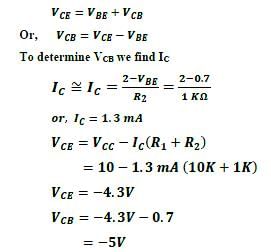
Test: Basic Electronics - 1 - Question 22

In the circuit as shown b = 99, VBE = 0.6 V, the what are the values of VC and IC corresponding to the operating point?

Test: Basic Electronics - 1 - Question 23

A silicon transistor with VBE sat = 0.8 V, b dc = 100 and VCE sat = 0.2 V is used in the circuit shown in given figure What is the minimum value of RC for which transistor is in saturation ?

Detailed Solution for Test: Basic Electronics - 1 - Question 23


Step 1

Apply kvl in 1 loop
5 - IbRb - 0.8 =0
5 - Ib*(200*1000ohm) - 0.8 =0
Base current (Ib)=(5-0.8)/(200*1000ohm)
=(4.2)/(200*1000)
=(2.1)/(100000)


2nd step

we know, collector current (Ic)= beta times of base current
so, Ic=(100*2.1)/(100000)=0.0021


3 step:-

Apply kvl in 2 loop
10 - 0.0021*Rc - 0.2 =0
minimum value of Rc is
Rc=(9.8)/(0.0021)
=4666.66ohm
=4667 ohm

Test: Basic Electronics - 1 - Question 24

The action of a JFET in its equivalent circuit can best be represented as a

Detailed Solution for Test: Basic Electronics - 1 - Question 24
The action of a JFET in its equivalent circuit can best be represented as a Voltage Controlled Current Source.
Explanation:
A JFET (Junction Field-Effect Transistor) is a three-terminal semiconductor device that can be used as an amplifier or as a switch in electronic circuits. In its equivalent circuit, the JFET can be represented by various models, such as the common-source model or the simple small-signal model.
The action of a JFET is best represented as a Voltage Controlled Current Source (VCCS) because of the following reasons:
1. Voltage-controlled device: The JFET operates based on the voltage applied to its gate terminal. The gate-source voltage controls the channel conductivity, which affects the current flow through the device. Therefore, the JFET can be considered a voltage-controlled device.
2. Current source behavior: In its active region of operation, the JFET can be approximated as a constant current source. The drain current is relatively independent of the drain-source voltage and is primarily determined by the gate-source voltage.
3. Output characteristics: The output characteristics of a JFET, represented by the drain current versus drain-source voltage curve, show a nearly constant current for a wide range of drain-source voltage values. This behavior is typical of a current source.
Therefore, the action of a JFET in its equivalent circuit can be best represented as a Voltage Controlled Current Source (VCCS). The JFET's drain current is controlled by the voltage applied to its gate terminal, making it a voltage-controlled device with current source behavior.
Test: Basic Electronics - 1 - Question 25

Consider the following statements: FETs when compared to BJTs have
1. high input impedance.
2. current flow due to majority carriers.
3. low input impedance
4. current flow due to minority carries.
Which of the statement given above are correct ?

Detailed Solution for Test: Basic Electronics - 1 - Question 25

The correct statements comparing FETs and BJTs are as follows:
1. FETs have high input impedance. FETs are voltage-controlled devices, which means that they require very little input current to control the output current. This results in a high input impedance, making FETs suitable for applications where the input signal is weak or where low power consumption is desired.
2. FETs have current flow due to majority carriers. FETs are unipolar devices, which means that the current flow is primarily due to the movement of majority carriers (either electrons or holes). In an n-channel FET, the current flow is due to the movement of electrons, while in a p-channel FET, the current flow is due to the movement of holes.
3. BJTs have low input impedance. Unlike FETs, BJTs are current-controlled devices, which means that they require a significant input current to control the output current. This results in a low input impedance, making BJTs suitable for applications where high current gain is desired.
4. BJTs have current flow due to minority carriers. BJTs are bipolar devices, which means that the current flow is due to the movement of minority carriers (either electrons or holes). In an NPN transistor, the current flow is due to the movement of minority electrons, while in a PNP transistor, the current flow is due to the movement of minority holes.
To summarize, FETs have high input impedance and current flow due to majority carriers, while BJTs have low input impedance and current flow due to minority carriers. Therefore, the correct statements are 1 and 2, which correspond to option D: 1 and 2.
23 videos|89 docs|42 tests
Information about Test: Basic Electronics - 1 Page
In this test you can find the Exam questions for Test: Basic Electronics - 1 solved & explained in the simplest way possible. Besides giving Questions and answers for Test: Basic Electronics - 1, EduRev gives you an ample number of Online tests for practice

Top Courses for Electrical Engineering (EE)

Download as PDF

Top Courses for Electrical Engineering (EE)