Electrical Engineering (EE) Exam  >  Electrical Engineering (EE) Tests  >  SSC JE Electrical Mock Test Series 2025  >  Test: Basic Electronics- 2 - Electrical Engineering (EE) MCQ

Test: Basic Electronics- 2 - Electrical Engineering (EE) MCQ


Test Description

20 Questions MCQ Test SSC JE Electrical Mock Test Series 2025 - Test: Basic Electronics- 2

Test: Basic Electronics- 2 for Electrical Engineering (EE) 2024 is part of SSC JE Electrical Mock Test Series 2025 preparation. The Test: Basic Electronics- 2 questions and answers have been prepared according to the Electrical Engineering (EE) exam syllabus.The Test: Basic Electronics- 2 MCQs are made for Electrical Engineering (EE) 2024 Exam. Find important definitions, questions, notes, meanings, examples, exercises, MCQs and online tests for Test: Basic Electronics- 2 below.
Solutions of Test: Basic Electronics- 2 questions in English are available as part of our SSC JE Electrical Mock Test Series 2025 for Electrical Engineering (EE) & Test: Basic Electronics- 2 solutions in Hindi for SSC JE Electrical Mock Test Series 2025 course. Download more important topics, notes, lectures and mock test series for Electrical Engineering (EE) Exam by signing up for free. Attempt Test: Basic Electronics- 2 | 20 questions in 12 minutes | Mock test for Electrical Engineering (EE) preparation | Free important questions MCQ to study SSC JE Electrical Mock Test Series 2025 for Electrical Engineering (EE) Exam | Download free PDF with solutions
Test: Basic Electronics- 2 - Question 1

At much lower temperature, semiconductors behave as:

Detailed Solution for Test: Basic Electronics- 2 - Question 1

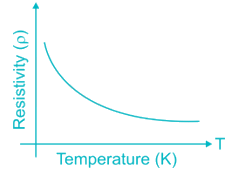
At lower temperatures, the electrons in valence band do not have sufficient energy to jump into conduction band. Thus carrier concentration decreases at lower temperatures and semiconductors behaves as insulators

Test: Basic Electronics- 2 - Question 2

In the silicon crystal structure, the recombination rate is proportional to the number of;

Detailed Solution for Test: Basic Electronics- 2 - Question 2

In an intrinsic semiconductor (un doped silicon) the number of electrons and the number of holes are equal. Hence recombination rate depends on both the number of electrons & number of holes.

In case of doped semiconductors, the recombination rate of the majority carriers are dependent on minority carrier density.

1 Crore+ students have signed up on EduRev. Have you? Download the App
Test: Basic Electronics- 2 - Question 3

The Fermi level Ein an intrinsic semiconductor, if effective masses of holes and electrons are same is:

Detailed Solution for Test: Basic Electronics- 2 - Question 3

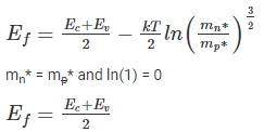
The fermi level (EF) in an intrinsic semiconductor is given by

Where Ec = Energy of conduction band minima

Ev = Energy of valence band maxima

K = Boltzman constant

T = Temperature

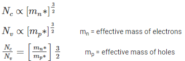
Nc = density of states in conduction band

Nv = density of states in valence band


Test: Basic Electronics- 2 - Question 4

Built- in potential Vof a junction depends on:

Detailed Solution for Test: Basic Electronics- 2 - Question 4

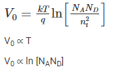
The built in potential V0 of a junction is given by

So built-in potential depends on both doping densities & temperature

Test: Basic Electronics- 2 - Question 5

During reverse bias operation of PN junction, a low current flows known as…….. which is……… barrier voltage:

Detailed Solution for Test: Basic Electronics- 2 - Question 5

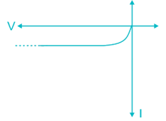
The reverse bias characteristics of a p – n junction diode is shown in the figure

From the figure it is clear that the reverse current is independent of voltage.

Test: Basic Electronics- 2 - Question 6

The depletion region of PN junction is consist of:

Detailed Solution for Test: Basic Electronics- 2 - Question 6

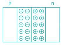
The holes from p-region cross the p-n Junction and recombine with electrons on the n-region. Similarly the electrons form n-region cross the junction & recombine with holes in p-region. Leaving immobile ions behind.

Thus the region near the junction is devoid of any mobile charge carriers, due to their recombination. Hence Depletion region of p-n Junction consists of immobile charges. 

Test: Basic Electronics- 2 - Question 7

A centre tapped full wave rectifier output contains only-

Detailed Solution for Test: Basic Electronics- 2 - Question 7

Since the output of full wave rectifier is an even function. Hence from Fourier series Analysis we know that even function have even harmonics thus output of FWR contains only even harmonics.

Test: Basic Electronics- 2 - Question 8

What is the effect on the diode current in a forward biased photo diode with increase in incident light intensity?

Detailed Solution for Test: Basic Electronics- 2 - Question 8

When the photodiode is forward biased it acts as a normal diode and the incident light intensity does not affect the diode current

Test: Basic Electronics- 2 - Question 9

Which diode has negative resistance region in its characteristics?

Detailed Solution for Test: Basic Electronics- 2 - Question 9

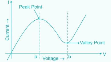
Tunnel diode characteristics

In Region between Peak Point & valley Point the current in Tunnel diode decrease with increase in forward Bias voltage. Thus Tunnel diode shows -ve resistance between peak point & valley point

Test: Basic Electronics- 2 - Question 10

The ripple factor of a power supply is a measure of

Detailed Solution for Test: Basic Electronics- 2 - Question 10

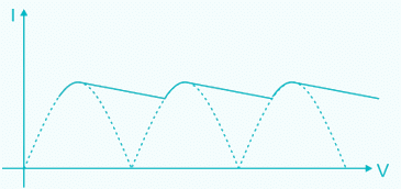
Thus if the ripple factor is less, the power supply has less AC components and power supply output is more pure (i.e more DC without much fluctuations)

Thus ripple factor is indication of purity of output of power supply

Test: Basic Electronics- 2 - Question 11

Which of the following diode is used for voltage stabilization?

Detailed Solution for Test: Basic Electronics- 2 - Question 11

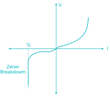
The I - V characteristic of Zener diode is shown

When Zener diode is reversed Biased the voltage across it is constant (V2).

Hence Zener Diode on reverse Biasing acts as voltage Stabilizer

Test: Basic Electronics- 2 - Question 12

Of the three BJT configurations CB, CE and CC:

Detailed Solution for Test: Basic Electronics- 2 - Question 12

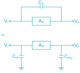
Av = gain of Amplifier

Miller Capacitance

CM = CC (1 + AV)

The increase in input capacitance decreases the upper cut off frequency

In case of CB configuration there is no miller capacitance between input and output & hence upper cut off frequency (fH) is high & higher Bandwidth

Test: Basic Electronics- 2 - Question 13

A transistor connected in common base configuration has:

Detailed Solution for Test: Basic Electronics- 2 - Question 13

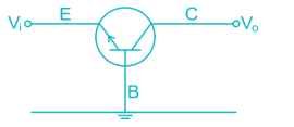
Input Terminal Emitter – Base (EB)

Output Terminal Collector – Base (CB)

Since for Amplification Application in BJT

EB Junction → Forward Biased (Low Impedance)

CB Junction → Reversed Biased (High Impedance)

Input Impedance is low

Output Impedance is high

Test: Basic Electronics- 2 - Question 14

Which of the following is not possible BJT configuration?

Detailed Solution for Test: Basic Electronics- 2 - Question 14

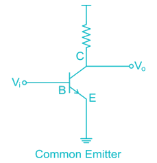
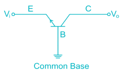
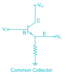
The 3 configurations in BJT are


The term “Common” refers to the Common terminal through which input is given and from which output is withdrawn i.e. common terminal between input and output.

The term common current is logically incorrect and is not a BJT Configuration.

Test: Basic Electronics- 2 - Question 15

When a BJT is used as switch, its mode of operation switches between:

Detailed Solution for Test: Basic Electronics- 2 - Question 15

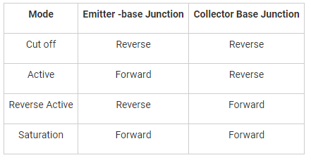
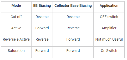
Different modes of BJT operations

For switching Application BJT is operated in cut off (off switch) and saturation (on switch)

Test: Basic Electronics- 2 - Question 16

For a transistor to act as current amplifier.

Detailed Solution for Test: Basic Electronics- 2 - Question 16

For any amplification, (voltage or current), the transistor should be operated in active region ie. emitter base junction is forward biased and collector base junction is reverse biased

Test: Basic Electronics- 2 - Question 17

The upper cut-off frequency of an RC coupled amplifier mainly depends upon:

Detailed Solution for Test: Basic Electronics- 2 - Question 17

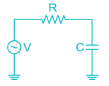
The Upper cut off frequency of R-C coupled multistage Amplifier is


Thus upper – cut off frequency depends on coupling capacitors

Test: Basic Electronics- 2 - Question 18

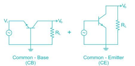
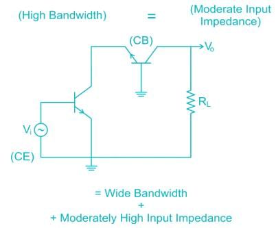
The cascade amplifier is a multistage configuration of:

Detailed Solution for Test: Basic Electronics- 2 - Question 18


Hence cascade is CE – CB Configuration

Test: Basic Electronics- 2 - Question 19

A Schottky diode is a

Detailed Solution for Test: Basic Electronics- 2 - Question 19

It is a majority carrier device. It is a semiconductor diode with a very fast switching action, but a low forward voltage drop. When a current flows through the diode there is a small voltage drop across the diode terminals. In a normal diode, the voltage drop is between 0.6 to 1.7 volts, while in a Schottky diode the voltage drop normally ranges between 0.15 and 0.45volts. This lower voltage drop provides higher switching speed and better system efficiency.

In Schottky diode, a semiconductor-metal junction is formed between a semiconductor and a metal, thus creating a Schottky barrier. The N-type semiconductor acts as a cathode and the metal side acts as the anode of the diode. The Schottky barrier diode is a unidirectional device conducting current flows only in one direction.

Test: Basic Electronics- 2 - Question 20

at room temperature intrinsic carrier concentration is higher in germanium than in silicon because __________.

Detailed Solution for Test: Basic Electronics- 2 - Question 20

Carrier concentrations depends on the energy gap in the intrinsic semiconductor. In the case of Ge and Si the intrinsic carrier concentration of Ge is higher than that of Si because the energy gap in Ge is smaller than that of Si.

2 videos|1 docs|55 tests
Information about Test: Basic Electronics- 2 Page
In this test you can find the Exam questions for Test: Basic Electronics- 2 solved & explained in the simplest way possible. Besides giving Questions and answers for Test: Basic Electronics- 2, EduRev gives you an ample number of Online tests for practice

Top Courses for Electrical Engineering (EE)

Download as PDF

Top Courses for Electrical Engineering (EE)